EP1396877B1 - Träger für elektronische Vorrichtungen, dessen Verfahren zur Herstellung, und elektronische Vorrichtung - Google Patents
Träger für elektronische Vorrichtungen, dessen Verfahren zur Herstellung, und elektronische Vorrichtung Download PDFInfo
- Publication number
- EP1396877B1 EP1396877B1 EP20030255438 EP03255438A EP1396877B1 EP 1396877 B1 EP1396877 B1 EP 1396877B1 EP 20030255438 EP20030255438 EP 20030255438 EP 03255438 A EP03255438 A EP 03255438A EP 1396877 B1 EP1396877 B1 EP 1396877B1
- Authority
- EP
- European Patent Office
- Prior art keywords
- substrate
- film
- forming
- buffer layer
- electronic devices
- Prior art date
- Legal status (The legal status is an assumption and is not a legal conclusion. Google has not performed a legal analysis and makes no representation as to the accuracy of the status listed.)
- Expired - Lifetime
Links
Images






Classifications
-
- H—ELECTRICITY
- H10—SEMICONDUCTOR DEVICES; ELECTRIC SOLID-STATE DEVICES NOT OTHERWISE PROVIDED FOR
- H10P—GENERIC PROCESSES OR APPARATUS FOR THE MANUFACTURE OR TREATMENT OF DEVICES COVERED BY CLASS H10
- H10P14/00—Formation of materials, e.g. in the shape of layers or pillars
- H10P14/60—Formation of materials, e.g. in the shape of layers or pillars of insulating materials
- H10P14/69—Inorganic materials
- H10P14/692—Inorganic materials composed of oxides, glassy oxides or oxide-based glasses
- H10P14/6938—Inorganic materials composed of oxides, glassy oxides or oxide-based glasses the material containing at least one metal element, e.g. metal oxides, metal oxynitrides or metal oxycarbides
- H10P14/6939—Inorganic materials composed of oxides, glassy oxides or oxide-based glasses the material containing at least one metal element, e.g. metal oxides, metal oxynitrides or metal oxycarbides characterised by the metal
- H10P14/69397—Inorganic materials composed of oxides, glassy oxides or oxide-based glasses the material containing at least one metal element, e.g. metal oxides, metal oxynitrides or metal oxycarbides characterised by the metal the material containing two or more metal elements
-
- H—ELECTRICITY
- H10—SEMICONDUCTOR DEVICES; ELECTRIC SOLID-STATE DEVICES NOT OTHERWISE PROVIDED FOR
- H10D—INORGANIC ELECTRIC SEMICONDUCTOR DEVICES
- H10D1/00—Resistors, capacitors or inductors
- H10D1/60—Capacitors
- H10D1/68—Capacitors having no potential barriers
- H10D1/682—Capacitors having no potential barriers having dielectrics comprising perovskite structures
-
- H—ELECTRICITY
- H10—SEMICONDUCTOR DEVICES; ELECTRIC SOLID-STATE DEVICES NOT OTHERWISE PROVIDED FOR
- H10D—INORGANIC ELECTRIC SEMICONDUCTOR DEVICES
- H10D1/00—Resistors, capacitors or inductors
- H10D1/60—Capacitors
- H10D1/68—Capacitors having no potential barriers
- H10D1/692—Electrodes
-
- H—ELECTRICITY
- H10—SEMICONDUCTOR DEVICES; ELECTRIC SOLID-STATE DEVICES NOT OTHERWISE PROVIDED FOR
- H10N—ELECTRIC SOLID-STATE DEVICES NOT OTHERWISE PROVIDED FOR
- H10N30/00—Piezoelectric or electrostrictive devices
- H10N30/01—Manufacture or treatment
- H10N30/07—Forming of piezoelectric or electrostrictive parts or bodies on an electrical element or another base
- H10N30/074—Forming of piezoelectric or electrostrictive parts or bodies on an electrical element or another base by depositing piezoelectric or electrostrictive layers, e.g. aerosol or screen printing
- H10N30/076—Forming of piezoelectric or electrostrictive parts or bodies on an electrical element or another base by depositing piezoelectric or electrostrictive layers, e.g. aerosol or screen printing by vapour phase deposition
-
- H—ELECTRICITY
- H10—SEMICONDUCTOR DEVICES; ELECTRIC SOLID-STATE DEVICES NOT OTHERWISE PROVIDED FOR
- H10N—ELECTRIC SOLID-STATE DEVICES NOT OTHERWISE PROVIDED FOR
- H10N30/00—Piezoelectric or electrostrictive devices
- H10N30/01—Manufacture or treatment
- H10N30/07—Forming of piezoelectric or electrostrictive parts or bodies on an electrical element or another base
- H10N30/074—Forming of piezoelectric or electrostrictive parts or bodies on an electrical element or another base by depositing piezoelectric or electrostrictive layers, e.g. aerosol or screen printing
- H10N30/079—Forming of piezoelectric or electrostrictive parts or bodies on an electrical element or another base by depositing piezoelectric or electrostrictive layers, e.g. aerosol or screen printing using intermediate layers, e.g. for growth control
-
- H—ELECTRICITY
- H10—SEMICONDUCTOR DEVICES; ELECTRIC SOLID-STATE DEVICES NOT OTHERWISE PROVIDED FOR
- H10N—ELECTRIC SOLID-STATE DEVICES NOT OTHERWISE PROVIDED FOR
- H10N30/00—Piezoelectric or electrostrictive devices
- H10N30/704—Piezoelectric or electrostrictive devices based on piezoelectric or electrostrictive films or coatings
- H10N30/706—Piezoelectric or electrostrictive devices based on piezoelectric or electrostrictive films or coatings characterised by the underlying bases, e.g. substrates
- H10N30/708—Intermediate layers, e.g. barrier, adhesion or growth control buffer layers
-
- H—ELECTRICITY
- H10—SEMICONDUCTOR DEVICES; ELECTRIC SOLID-STATE DEVICES NOT OTHERWISE PROVIDED FOR
- H10N—ELECTRIC SOLID-STATE DEVICES NOT OTHERWISE PROVIDED FOR
- H10N30/00—Piezoelectric or electrostrictive devices
- H10N30/80—Constructional details
- H10N30/87—Electrodes or interconnections, e.g. leads or terminals
- H10N30/877—Conductive materials
- H10N30/878—Conductive materials the principal material being non-metallic, e.g. oxide or carbon based
-
- H—ELECTRICITY
- H10—SEMICONDUCTOR DEVICES; ELECTRIC SOLID-STATE DEVICES NOT OTHERWISE PROVIDED FOR
- H10P—GENERIC PROCESSES OR APPARATUS FOR THE MANUFACTURE OR TREATMENT OF DEVICES COVERED BY CLASS H10
- H10P14/00—Formation of materials, e.g. in the shape of layers or pillars
- H10P14/60—Formation of materials, e.g. in the shape of layers or pillars of insulating materials
- H10P14/63—Formation of materials, e.g. in the shape of layers or pillars of insulating materials characterised by the formation processes
- H10P14/6326—Deposition processes
- H10P14/6349—Deposition of epitaxial materials
-
- H—ELECTRICITY
- H10—SEMICONDUCTOR DEVICES; ELECTRIC SOLID-STATE DEVICES NOT OTHERWISE PROVIDED FOR
- H10P—GENERIC PROCESSES OR APPARATUS FOR THE MANUFACTURE OR TREATMENT OF DEVICES COVERED BY CLASS H10
- H10P14/00—Formation of materials, e.g. in the shape of layers or pillars
- H10P14/60—Formation of materials, e.g. in the shape of layers or pillars of insulating materials
- H10P14/65—Formation of materials, e.g. in the shape of layers or pillars of insulating materials characterised by treatments performed before or after the formation of the materials
- H10P14/6502—Formation of materials, e.g. in the shape of layers or pillars of insulating materials characterised by treatments performed before or after the formation of the materials of treatments performed before formation of the materials
- H10P14/6504—In-situ cleaning
-
- H—ELECTRICITY
- H10—SEMICONDUCTOR DEVICES; ELECTRIC SOLID-STATE DEVICES NOT OTHERWISE PROVIDED FOR
- H10P—GENERIC PROCESSES OR APPARATUS FOR THE MANUFACTURE OR TREATMENT OF DEVICES COVERED BY CLASS H10
- H10P14/00—Formation of materials, e.g. in the shape of layers or pillars
- H10P14/60—Formation of materials, e.g. in the shape of layers or pillars of insulating materials
- H10P14/65—Formation of materials, e.g. in the shape of layers or pillars of insulating materials characterised by treatments performed before or after the formation of the materials
- H10P14/6502—Formation of materials, e.g. in the shape of layers or pillars of insulating materials characterised by treatments performed before or after the formation of the materials of treatments performed before formation of the materials
- H10P14/6512—Formation of materials, e.g. in the shape of layers or pillars of insulating materials characterised by treatments performed before or after the formation of the materials of treatments performed before formation of the materials by exposure to a gas or vapour
-
- H—ELECTRICITY
- H10—SEMICONDUCTOR DEVICES; ELECTRIC SOLID-STATE DEVICES NOT OTHERWISE PROVIDED FOR
- H10P—GENERIC PROCESSES OR APPARATUS FOR THE MANUFACTURE OR TREATMENT OF DEVICES COVERED BY CLASS H10
- H10P14/00—Formation of materials, e.g. in the shape of layers or pillars
- H10P14/60—Formation of materials, e.g. in the shape of layers or pillars of insulating materials
- H10P14/65—Formation of materials, e.g. in the shape of layers or pillars of insulating materials characterised by treatments performed before or after the formation of the materials
- H10P14/6502—Formation of materials, e.g. in the shape of layers or pillars of insulating materials characterised by treatments performed before or after the formation of the materials of treatments performed before formation of the materials
- H10P14/6512—Formation of materials, e.g. in the shape of layers or pillars of insulating materials characterised by treatments performed before or after the formation of the materials of treatments performed before formation of the materials by exposure to a gas or vapour
- H10P14/6514—Formation of materials, e.g. in the shape of layers or pillars of insulating materials characterised by treatments performed before or after the formation of the materials of treatments performed before formation of the materials by exposure to a gas or vapour by exposure to a plasma
-
- H—ELECTRICITY
- H03—ELECTRONIC CIRCUITRY
- H03H—IMPEDANCE NETWORKS, e.g. RESONANT CIRCUITS; RESONATORS
- H03H3/00—Apparatus or processes specially adapted for the manufacture of impedance networks, resonating circuits, resonators
- H03H3/007—Apparatus or processes specially adapted for the manufacture of impedance networks, resonating circuits, resonators for the manufacture of electromechanical resonators or networks
- H03H3/02—Apparatus or processes specially adapted for the manufacture of impedance networks, resonating circuits, resonators for the manufacture of electromechanical resonators or networks for the manufacture of piezoelectric or electrostrictive resonators or networks
-
- H—ELECTRICITY
- H10—SEMICONDUCTOR DEVICES; ELECTRIC SOLID-STATE DEVICES NOT OTHERWISE PROVIDED FOR
- H10N—ELECTRIC SOLID-STATE DEVICES NOT OTHERWISE PROVIDED FOR
- H10N30/00—Piezoelectric or electrostrictive devices
- H10N30/01—Manufacture or treatment
- H10N30/08—Shaping or machining of piezoelectric or electrostrictive bodies
- H10N30/082—Shaping or machining of piezoelectric or electrostrictive bodies by etching, e.g. lithography
-
- H—ELECTRICITY
- H10—SEMICONDUCTOR DEVICES; ELECTRIC SOLID-STATE DEVICES NOT OTHERWISE PROVIDED FOR
- H10P—GENERIC PROCESSES OR APPARATUS FOR THE MANUFACTURE OR TREATMENT OF DEVICES COVERED BY CLASS H10
- H10P14/00—Formation of materials, e.g. in the shape of layers or pillars
- H10P14/40—Formation of materials, e.g. in the shape of layers or pillars of conductive or resistive materials
-
- H—ELECTRICITY
- H10—SEMICONDUCTOR DEVICES; ELECTRIC SOLID-STATE DEVICES NOT OTHERWISE PROVIDED FOR
- H10P—GENERIC PROCESSES OR APPARATUS FOR THE MANUFACTURE OR TREATMENT OF DEVICES COVERED BY CLASS H10
- H10P14/00—Formation of materials, e.g. in the shape of layers or pillars
- H10P14/60—Formation of materials, e.g. in the shape of layers or pillars of insulating materials
- H10P14/63—Formation of materials, e.g. in the shape of layers or pillars of insulating materials characterised by the formation processes
- H10P14/6326—Deposition processes
- H10P14/6342—Liquid deposition, e.g. spin-coating, sol-gel techniques or spray coating
-
- H—ELECTRICITY
- H10—SEMICONDUCTOR DEVICES; ELECTRIC SOLID-STATE DEVICES NOT OTHERWISE PROVIDED FOR
- H10P—GENERIC PROCESSES OR APPARATUS FOR THE MANUFACTURE OR TREATMENT OF DEVICES COVERED BY CLASS H10
- H10P14/00—Formation of materials, e.g. in the shape of layers or pillars
- H10P14/60—Formation of materials, e.g. in the shape of layers or pillars of insulating materials
- H10P14/66—Formation of materials, e.g. in the shape of layers or pillars of insulating materials characterised by the type of materials
- H10P14/662—Laminate layers, e.g. stacks of alternating high-k metal oxides
-
- H—ELECTRICITY
- H10—SEMICONDUCTOR DEVICES; ELECTRIC SOLID-STATE DEVICES NOT OTHERWISE PROVIDED FOR
- H10P—GENERIC PROCESSES OR APPARATUS FOR THE MANUFACTURE OR TREATMENT OF DEVICES COVERED BY CLASS H10
- H10P14/00—Formation of materials, e.g. in the shape of layers or pillars
- H10P14/60—Formation of materials, e.g. in the shape of layers or pillars of insulating materials
- H10P14/69—Inorganic materials
- H10P14/692—Inorganic materials composed of oxides, glassy oxides or oxide-based glasses
- H10P14/6938—Inorganic materials composed of oxides, glassy oxides or oxide-based glasses the material containing at least one metal element, e.g. metal oxides, metal oxynitrides or metal oxycarbides
- H10P14/69398—Inorganic materials composed of oxides, glassy oxides or oxide-based glasses the material containing at least one metal element, e.g. metal oxides, metal oxynitrides or metal oxycarbides the material having a perovskite structure, e.g. BaTiO3
Definitions
- the present invention relates to a substrate for electronic devices, a manufacturing method therefor, and an electronic device. More specifically, the substrate for electronic devices according to the present invention is preferably used for mounting thereon a ferroelectric element functioning as a capacitor, a piezoelectric element functioning as a cantilever, or the like.
- Ferroelectric memories are divided into; a capacitor type using a ferroelectric as a capacitor, formed in a 1T (transistor)/1C (capacitor) structure, and an MFSFET (Metal Ferroelectric Semiconductor Field Effect Transistor) type using a ferroelectric as a gate insulating film for a field-effect transistor instead of SiO 2 .
- the MFSFET type is more advantageous than the capacitor type in view of high integration and non-destructive reading, but it has not yet been realized due to difficulty in manufacturing related to the structure. Hence, development and commercialization of the capacitor type is ahead at present.
- Representative ferroelectric materials adopted in the capacitor type ferroelectric memory include PbZr 1-x Ti x O 3 (abbreviated as PZT) and SrBi 2 Ta 2 O 9 (abbreviated as SBT).
- PZT PbZr 1-x Ti x O 3
- SBT SrBi 2 Ta 2 O 9
- MPB Magnetic Phase Boundary
- the capacitor type ferroelectric memory has a structure in which the ferroelectric material PZT, is placed between a lower electrode and an upper electrode.
- Pt has heretofore been used as a material forming the lower electrode.
- Pt has strong self-orientation, and is oriented in a cubic (111) direction even on a thin film having an amorphous structure, such as SiO 2 , and is hence used preferably.
- SiO 2 amorphous structure
- Ti is used for improving the bond between Pt and SiO 2
- TiN is used for preventing Pb from diffusing, in many cases.
- the lower electrode has a complicated electrode structure, causing oxidation of Ti and diffusion of Ti into Pt, accompanied with deterioration in crystallinity of PZT.
- P-E polarization - electric field
- PZT in this composition range exhibits a tetragonal, and the polarization direction thereof is parallel with the C-axis.
- the buffer layer epitaxially grown on the Si substrate includes oxides having a fluorite structure, such as yttria stabilized zirconia (abbreviation: YSZ, Zr 1-x Y x O 2-0.5x ) and CeO 2 .
- YSZ yttria stabilized zirconia
- CeO 2 CeO 2
- the present inventors have conducted research and development for a case where a YSZ buffer layer is used, and the SrRuO 3 electrode is grown epitaxially thereon, and as a result, it has been found that this structure has two problems described below.
- the first problem is that in order to grow a buffer layer such as YSZ and CeO 2 on the Si substrate epitaxially, predetermined surface treatment is necessary with respect to a film-forming surface of the Si substrate, before deposition of the buffer layer thereon.
- this surface treatment method two methods are well known, that is, a method of forming a reconstructed surface, and a method of forming a hydrogen-terminated surface.
- a technique in which a surface of the Si substrate is changed to a hydrogen-terminated surface, by subjecting the surface of the Si substrate to a treatment by hydrofluoric acid is disclosed in non-patent document 3.
- the reconstructed surface represents a surface in which the periodic structure of the surface has been changed to bulk, by performing heat treatment in a high temperature and high vacuum atmosphere, so as to allow excessive covalent bonds (dangling bonds) in Si atoms forming the surface layer of the Si substrate to bond with each other.
- the hydrogen-terminated surface stands for a surface having a structure in which after an SiO 2 natural oxide film forming the surface layer of the Si substrate is etched by washing with hydrofluoric acid, the dangling bonds on the surface are terminated with hydrogen in ammonium fluoride solution.
- Non-Patent Document 3 (Non-Patent Document 3)
- the second problem is that the orientation direction of SrRuO 3 formed on the buffer layer changes to the (110) orientation (pseudo-cubic).
- Non-Patent Document 4 (Non-Patent Document 4)
- predetermined surface treatment has heretofore been required with respect to the film-forming surface of the Si substrate, before deposition of the buffer layer thereon, thereby causing complication of the manufacturing process and an increase in the manufacturing cost. Even if such predetermined surface treatment is conducted, the epitaxial growth of the buffer layer formed thereon cannot be realized in the desired (100) orientation, but only the epitaxial growth in the (110) orientation can be realized.
- the substrate comprises an La 0.5 Sr 0.5 CoO 3 (LSCO) top electrode disposed on top of a film of Bi 4 Ti 3 O 12 , which is deposited on a CeO 2 /YSZ/Si multilayer template.
- the multilayer template comprises an SiO 2 epitaxial layer on a Si(100) base.
- United States Patent No. 5,270,298 describes a method of forming crystalline metal-oxide thin films on silicon and the resultant structure.
- a crystalline buffer layer of yttria-stabilized zirconia is deposited on a silicon substrate.
- a thin template layer of an anisotropic perovskite, such as bismuth titanate or yttria barium copper oxide, is deposited on the template layer under conditions favouring c-axis oriented growth.
- a nominally cubic metal-oxide layer is deposited on the template layer, which facilitates its singly crystalline growth.
- the metal oxide is nominally a cubic perovskite, but may be a conductive electrode, a ferroelectric, a non-hysteretic dielectric, a piezoelectric, or other class of material.
- a substrate for electronic devices in which when a buffer layer such as YSZ and CeO 2 is grown epitaxially on an Si substrate, predetermined surface treatment, that is, treatment for forming a reconstructed surface or treatment for forming a hydrogen-terminated surface is not necessary with respect to the film-forming surface of the Si substrate, before deposition of the buffer layer thereon, and even if the predetermined surface treatment is not performed, the buffer layer can be epitaxially grown in the (100) orientation, and a manufacturing method therefor.
- predetermined surface treatment that is, treatment for forming a reconstructed surface or treatment for forming a hydrogen-terminated surface is not necessary with respect to the film-forming surface of the Si substrate, before deposition of the buffer layer thereon, and even if the predetermined surface treatment is not performed, the buffer layer can be epitaxially grown in the (100) orientation, and a manufacturing method therefor.
- the present invention provides a substrate for electronic devices comprising: a substrate consisting of silicon, and a first buffer layer, a second buffer layer, a first oxide electrode layer and a second oxide electrode layer, which are grown epitaxially and laminated in this order on the film-forming surface of the substrate, wherein the first buffer layer is a first metal oxide having a fluorite structure, the second buffer layer is a second metal oxide having a fluorite structure, the first oxide electrode layer is a third metal oxide having a layered perovskite structure, and the second oxide electrode layer is a fourth metal oxide having a simple perovskite structure.
- the present invention provides a manufacturing method for the substrate for electronic devices, comprising:
- a substrate for electronic devices having a construction such that the first buffer layer and the second buffer layer having the fluorite structure are grown epitaxially in the cubic (100) orientation on the Si substrate, the first oxide electrode layer having the layered perovskite structure is grown epitaxially in a tetragonal or orthorhombic (001) orientation thereon, and the second oxide electrode layer having the simple perovskite structure is grown epitaxially in a cubic or pseudo-cubic (100) orientation thereon.
- the outermost surface is the (100) oriented second oxide electrode layer
- the epitaxial growth of the ferroelectric layer or the piezoelectric layer can be realized easily in the tetragonal (001) orientation or a rhombohedral (100) orientation.
- electronic devices provided with functional elements such as a ferroelectric memory or a piezoelectric element formed by providing a ferroelectric layer or a piezoelectric layer on the substrate, can be made with an optimal construction.
- the first buffer layer having the fluorite structure when the first buffer layer having the fluorite structure is formed on the Si substrate, the first buffer layer is grown epitaxially at a higher rate than the growth rate of SiO 2 , by irradiating a metallic element gas or plasma onto the Si substrate coated with a natural oxide film in an SiO sublimation area, so that the first buffer layer can be formed, without forming a thermally oxidized amorphous layer between the Si substrate and the first buffer layer.
- the first buffer layer having a desired oriented plane and excellent crystallinity can be formed, thereby enabling the second buffer layer, the first oxide electrode layer and the second oxide electrode layer formed on the first buffer layer to have excellent crystallinity.
- a substrate for electronic devices enabling production of high performance electronic devices can be manufactured.
- FIG. 1 is a schematic sectional view of the substrate for electronic devices according to the present invention.
- the substrate 100 for electronic devices comprises a substrate 11 consisting of silicon, and a first buffer layer 12, a second buffer layer 13, a first oxide electrode layer 14 and a second oxide electrode layer epitaxially grown and laminated in this order on a film-forming surface of the substrate 11.
- the first buffer layer 12 is a first metal oxide having a fluorite structure
- the second buffer layer 13 is a second metal oxide having a fluorite structure
- the first oxide electrode layer 14 is a third metal oxide having a layered perovskite structure
- the second oxide electrode layer 15 is a fourth metal oxide having a simple perovskite structure.
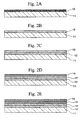
- FIGS. 2A to 2E are schematic sectional views illustrating states in which the first buffer layer 12, the second buffer layer 13, the first oxide electrode layer 14 and the second oxide electrode layer 15 are sequentially laminated on the substrate 11, when the substrate for electronic devices in FIG. 1 is manufactured.
- FIG. 2A illustrates the substrate 11 immediately before the first buffer layer 12 is provided, indicating that an oxide layer 16 exists on the film-forming surface.
- FIG. 2B represents the state where the first buffer layer 12 is provided
- FIG. 2C represents the state where second buffer layer 13 is provided
- FIG. 2D represents the state where the first oxide electrode layer 14 is provided
- FIG. 2E represents the state where the second oxide electrode layer 15 is provided.
- the first metal oxide having the fluorite structure is first provided as the first buffer layer 12, on the film-forming surface of the substrate 11 consisting of silicon. So long as this is the first metal oxide having the fluorite structure, then even if the film-forming surface of the substrate 11 consisting of silicon has not been subjected to predetermined surface treatment, that is, the treatment for forming a reconstructed surface or the treatment for forming a hydrogen-terminated surface, epitaxial growth of the first buffer layer 12 comprising the first metal oxide becomes possible.
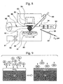
- FIG. 9 is a schematic sectional view illustrating this situation.
- the left figure represents the state in which oxygen remains on the film-forming surface of the substrate 11, with the film-forming surface of the substrate 11 covered with SiO 2 .
- the right figure represents the state in which on adherence of the metal oxide thereon, oxygen disengages from the film-forming surface of the substrate 11 in the form of SiO, and as a result, YSZ grows epitaxially as the first buffer layer 12.
- the material by which the above phenomenon can be confirmed is a metal oxide having the fluorite structure.
- the fluorite structure is as shown in FIG. 10 .
- the metal oxide forming the first buffer layer 12 is referred to as a first metal oxide. It has been confirmed by X-ray photoelectron spectroscopy (abbreviated as XPS) that oxygen remains on the film-forming surface of the substrate 11, which has not undergone the predetermined surface treatment.
- XPS X-ray photoelectron spectroscopy
- the present inventors have confirmed by experiments that the above phenomenon occurs when the orientation of the film-forming surface of the substrate 11 consisting of silicon is (100), (110) or (111).
- the film-forming surface of the substrate 11 consisting of silicon when the above phenomenon occurs that is, the film-forming surface that has not been subjected to the predetermined surface treatment, such as the treatment for forming a reconstructed surface or the treatment for forming a hydrogen-terminated surface, can be specified, since a diffraction pattern is not observed in a diffraction image by the RHEED method, before forming the first buffer layer.
- FIGS. 3A to 3E are photographs of diffraction images observed by the RHEED method.
- FIG. 3A shows the result of observing the surface where the oxide layer 16 exists on the substrate 11, immediately before the first buffer layer 12 is formed.
- FIG. 3B to FIG. 3E respectively show the results of observation of the surfaces of the first buffer layer 12, the second buffer layer 13, the first oxide electrode layer 14, and the second oxide electrode layer 15.
- the second buffer layer 13 comprising the second metal oxide having the fluorite structure
- the first oxide electrode layer 14 comprising the third metal oxide having the layered perovskite structure
- the second oxide electrode layer 15 comprising the fourth metal oxide having the simple perovskite structure
- the second oxide electrode layer 15 laminated last can epitaxially grow in the (100) orientation, which has been a difficult orientation.
- FIG. 11 illustrates an example of the simple perovskite structure
- FIG. 12 and FIG. 13 illustrate examples of the layered perovskite structure.
- the substrate for electronic devices having the above configuration comprises an oxide electrode layer epitaxially grown in the (100) orientation on the outermost surface
- the ferroelectric material comprising PZT or SBT can be grown as a (001) oriented film thereon. Therefore, the substrate for electronic devices according to the present invention is suitable as a substrate for manufacturing ferroelectric elements and piezoelectric elements.
- the first metal oxide constituting the first buffer layer 12 is, for example, a solid solution expressed as Zr 1-x M ⁇ x O y (0 ⁇ x ⁇ 1, 1.5 ⁇ y ⁇ 2) obtained by substituting a part of Zr, being a constituent element of zirconia, by a metal element M ⁇ (where M ⁇ indicates one kind of element selected from La, Ce, Pr, Nd, Pm, Sm, Eu, Gd, Tb, Dy, Ho, Er, Tm, Yb, Lu, Y, Mg, Ca, Sr and Ba), and is preferably cubically oriented in the (100) direction.
- M ⁇ indicates one kind of element selected from La, Ce, Pr, Nd, Pm, Sm, Eu, Gd, Tb, Dy, Ho, Er, Tm, Yb, Lu, Y, Mg, Ca, Sr and Ba
- the second metal oxide constituting the second buffer layer 13 is cerium oxide or a solid solution expressed as Ce 1-x M ⁇ x O y (0 ⁇ x ⁇ 1, 1.5 ⁇ y ⁇ 2) obtained by substituting a part of Ce, being a constituent element of cerium oxide, by a metal element M ⁇ (where M ⁇ indicates one kind of element selected from Zr, La, Pr, Nd, Pm, Sm, Eu, Gd, Tb, Dy, Ho, Er, Tm, Yb, Lu, Y, Mg, Ca, Sr and Ba), and is preferably cubically oriented in the (100) direction.
- the third metal oxide constituting the first oxide electrode layer 14 is a solid solution containing a metal element M ⁇ or RE as a constituent element, and expressed as M ⁇ RuO 4, RE 2 NiO 4, or REBa 2 Cu 3 O x (where M ⁇ indicates one kind of element selected from Ca, Sr and Ba, and RE indicates one kind of element selected from La, Ce, Pr, Nd, Pm, Sm, Eu, Gd, Tb, Dy, Ho, Er, Tm, Yb, Lu, and Y), and is preferably tetragonally or orthorhombically oriented in the (001) direction.
- M ⁇ indicates one kind of element selected from Ca, Sr and Ba
- RE indicates one kind of element selected from La, Ce, Pr, Nd, Pm, Sm, Eu, Gd, Tb, Dy, Ho, Er, Tm, Yb, Lu, and Y
- M ⁇ indicates one kind of element selected from Ca, Sr and Ba
- RE indicates one kind of element selected from La, Ce, Pr, Nd,
- the fourth metal oxide constituting the second oxide electrode layer 15 is a solid solution containing a metal element M ⁇ or RE as a constituent element, and expressed as M ⁇ RuO 3 , (RE, M ⁇ )CrO 3 , (RE, M ⁇ )MnO 3 , (RE, M ⁇ )CoO 3 , or (RE, M ⁇ )NiO 3 (where M ⁇ indicates one kind of element selected from Ca, Sr and Ba, and RE indicates one kind of element selected from La, Ce, Pr, Nd, Pm, Sm, Eu, Gd, Tb, Dy, Ho, Er, Tm, Yb, Lu, and Y), and is preferably cubically or pseudo-cubically oriented in the (100) direction.
- FIG. 7 is a flowchart for each step constituting a manufacturing method for a substrate for electronic devices according to the present invention.
- the manufacturing method for a substrate for electronic devices comprises: a pretreatment step for washing the substrate 11 consisting of silicon (in FIG. 7 , expressed as "Si substrate washing step");
- FIG. 8 is a schematic sectional view of the film-forming apparatus which forms a thin film by a pulsed laser deposition (PLD) method, wherein reference symbol 80 denotes a process chamber, whose inside can be decompressed, 81 denotes a rotatable base metal supporting section having film-forming base metals placed thereon, referred to as targets, 82 denotes a target placed on the base metal supporting section 81, 83 denotes a substrate holding section, 84 denotes a temperature control section built into the substrate holding section 83, 85 denotes a substrate, 86 denotes a thin film deposited on the substrate 85, 87 denotes an introduction pipe for a process gas, 88 denotes an opening and closing mechanism for controlling the process gas, 89 denotes an (ArF or KrF) exc
- PLD pulsed laser deposition
- the PLD method used in the film-forming apparatus shown in FIG. 8 is a film-forming method in which an excimer laser beam is irradiated onto a rotating target in the form of pulses, in an oxygen atmosphere in which the inside space of the process chamber 80 is kept at a very low pressure, for example, at a pressure of about 1/1000 of atmospheric pressure, while forming the thin film 86 on the substrate 85, so that the component constituting the target is made fly to the substrate in a plasma or molecular state by this irradiation, thereby depositing the thin film on the film-forming surface of the substrate.
- the pretreatment step stands for washing treatment for removing organics from the surface layer of the substrate 11 consisting of silicon, and drying treatment conducted thereafter.
- this washing treatment for example, the substrate 11 is soaked in an organic solvent, or ultrasonic waves are applied simultaneously with soaking, to remove organics adhered to the substrate 11.
- the drying treatment is for removing the organic solvent used in the washing treatment, from the film-forming surface of the substrate 11.
- this pretreatment step it is desired to finish the film-forming surface of the substrate 11 as a surface where the oxide layer 16 exists, not as a reconstructed surface or a hydrogen-terminated surface.
- the RCA washing or washing with hydrofluoric acid for obtaining the reconstructed surface or the hydrogen-terminated surface which has been heretofore conducted after the washing treatment using the organic solvent, is not conducted, so as to finish the film-forming surface of the substrate 11 in a state with oxygen (oxide layer 16) remaining thereon ( FIG. 2A ).
- the substrate 11 having undergone the pretreatment step is arranged in a film-forming container under a reduced-pressure atmosphere, and a predetermined gas or plasma is irradiated onto the film-forming surface of the substrate 11, to epitaxially grow the first buffer layer 12 comprising the first metal oxide having the fluorite structure.
- the predetermined gas or plasma comprises an element constituting the metal oxide to be formed in the first film-forming step, and this is irradiated onto the film-forming surface of the substrate 11.
- Oxygen (the oxide layer 16) remains on the film-forming surface of the substrate 11 produced in the pretreatment step, and the film-forming surface is covered with SiO 2 Therefore, when this film-forming surface is exposed to the gas or plasma comprising the element constituting the metal oxide, the element adheres to the film-forming surface, so that the metal oxide starts to deposite, and at the same time, the SiO 2 film forming the oxide layer 16 existing on the film-forming surface is sublimated in the form of SiO and removed from the film-forming surface struck by the gas or plasma.
- the substrate 11 is held under a temperature, a back pressure, and an oxygen partial pressure such that the vapor pressure of SiO does not reach the saturated vapor pressure, and the deposition rate of the first buffer layer 12 is set to not lower than a growth rate of the thermally oxidized SiO 2 film on the film-forming surface of the substrate 11.
- the metal oxide having the fluorite structure is preferably used for the first buffer layer, since the above action can be stably obtained.
- the deposition rate of the first buffer layer 12 is preferably set to not lower than the growth rate (0.2 nm/min.) of the thermally oxidized SiO 2 film.
- the film-forming conditions for obtaining this deposition rate is such that the density of the laser energy is not lower than 1 J/cm 2 , the laser frequency is not lower than 5 Hz, and the target-substrate distance is from 50 mm to 80 mm inclusive.
- the deposition rate of the first buffer layer 12 it is important to set the deposition rate of the first buffer layer 12 to not lower than the growth rate (0.2 nm/min.) of the thermally oxidized SiO 2 film. This is because, from a verification experiment by the present inventors relating to the relation between the deposition rate and the crystallinity of the first buffer layer, it was found that when the deposition rate was lower than 0.2 nm/min, which is the growth rate of the thermally oxidized SiO 2 film, the epitaxial growth of the first buffer layer 12 could not be achieved. The details of the verification experiment are described below.
- the experiment was conducted by preparing a pretreated Si substrate, and forming a YSZ film on the Si substrate as the first buffer layer by the PLD method using the film-forming apparatus shown in FIG. 8 .
- the deposition rate of YSZ was adjusted by variously changing the laser frequency, the target-substrate distance and the laser energy density.
- the respective experiment conditions, the deposition rate of YSZ, and the full width at half maximum (FWHM) in a rocking curve of a YSZ (200) peak obtained by measuring the formed YSZ by the XRD are shown in Table 1.
- the substrate temperature at the time of film forming was 700°C
- the back pressure in the film-forming atmosphere was 1.33 ⁇ 10 -4 Pa (1 ⁇ 10 -6 Torr)
- the oxygen partial pressure was 6.6 ⁇ 10 -3 Pa (5 ⁇ 10 -5 Torr), which were common in all conditions.
- FIG. 14 is a graph in which the results shown in Table 1 are itemized for each parameter used for the adjustment of the deposition rate.
- the deposition rate of YSZ is plotted on the X axis
- the peak half width of YSZ (200) is plotted on the Y axis.
- the peak half width of YSZ (200) is extremely large, indicating that YSZ has not epitaxially grown.
- the peak half width becomes narrow, and YSZ has epitaxially grown favorably.
- the reaction which inhibits the epitaxial growth of YSZ on the Si substrate progresses on the Si substrate.
- This deposition rate of 0.2 nm/min. substantially agrees with the deposition rate of the thermally oxidized SiO 2 film on the Si substrate, and the deposition process of YSZ is conducted in an oxygen-containing atmosphere by heating the substrate to a high temperature. Therefore, it can be presumed that the reaction inhibiting the epitaxial growth of YSZ is a reaction for forming the thermally oxidized SiO 2 film on the surface of the Si substrate.
- the first buffer layer 12 since the above described action operates, it is not necessary to increase the substrate temperature more than necessary, or set the back pressure in the film-forming atmosphere to ultra-high vacuum.
- a substrate having a film-forming surface comprising a reconstructed surface or a hydrogen-terminated surface is used, and the first buffer layer is formed thereon.
- a substrate temperature exceeding 800°C and a film-forming atmosphere in which the back pressure is lower than 1.33 ⁇ 10 -4 Pa (1 ⁇ 10 -6 Torr) are the essential conditions. Therefore, according to the first film-forming step of the present invention, the energy required for producing the first buffer layer 12 can be considerably reduced, thereby contributing to a reduction in the production cost.
- a predetermined gas or plasma is irradiated onto the surface of the first buffer layer 12 formed in the first film-forming step, to epitaxially grow the second buffer layer 13 comprising the second metal oxide having the fluorite structure.
- the second buffer layer 13 there is selected one comprising the second metal oxide, being a different material from that of the first metal oxide constituting the first buffer layer 12, and having an effect of stimulating the epitaxial growth of the first oxide electrode layer 14 to be laminated on the second buffer layer 13.
- the droplet particles may be removed by adding a step of wiping off the surface of the first buffer layer 12, using a flexible material or a member having a flexible structure.
- the droplet particles of about 100 to 1000 pcs./cm 2 exist before removal, the number thereof can be decreased up to 0.1 to 1 pcs/cm 2 after removal, by using a cotton bud as the above member.
- the removal of the droplet particles generated on the surface of the first buffer layer 12 stimulates the epitaxial growth of the second buffer layer 13 formed thereon, thereby contributing to ensure the flatness.
- a predetermined gas or plasma is irradiated onto the surface of the second buffer layer 13 formed in the second film-forming step, to epitaxially grow the first oxide electrode layer 14 comprising the third metal oxide having the layered perovskite structure.
- a predetermined gas or plasma is irradiated onto the surface of the first oxide electrode layer 14 formed in the third film-forming step, to epitaxially grow the second oxide electrode layer 15 comprising the fourth metal oxide having the simple perovskite structure.
- the first oxide electrode layer 14 comprising the third metal oxide having the layered perovskite structure is not provided, but the second oxide electrode layer 15 comprising the fourth metal oxide having the simple perovskite structure is directly formed on the surface of the second buffer layer 12.
- the outermost surface is oriented in the (110) direction.
- an oxide electrode layer epitaxially grown in the (100) orientation can be formed on the outermost surface.
- the first oxide electrode layer 14 there is selected one comprising the third metal oxide, being a different material from that of the second metal oxide constituting the second buffer layer 13, and having an effect of stimulating the epitaxial growth of the second oxide electrode layer 15 to be laminated on the first oxide electrode layer 14.
- the second oxide electrode layer 15 one that epitaxially grows on the first oxide electrode layer 14, and is oriented in the (100) direction is selected.
- a predetermined gas or plasma comprising an element constituting the metal oxide to be formed in each step is used.
- the first film-forming step when a gas or plasma generated by irradiating a laser beam onto a base metal arranged opposite to the film-forming surface of the substrate 11 is used as the predetermined gas or plasma, it is desired to irradiate the gas or plasma of the constituent element of the first buffer layer 12 onto the substrate 11 held under a temperature, a back pressure and an oxygen partial pressure such that the vapor pressure of SiO does not reach the saturated vapor pressure, so that an SiO 2 film forming the oxide layer 16 existing on the film-forming surface of the substrate 11 is reduced to Si.
- the first buffer layer 12 is deposited on the film-forming surface at an deposition rate not lower than the rate at which the thermally oxidized SiO 2 film is formed, while sublimating and removing the Si formed by reduction as SiO, so that the first buffer layer 12 is epitaxially grown, without forming an amorphous layer on the interface between the substrate 11 and the first buffer layer 12. If formed in this manner, the first buffer layer 12 having a desired orientation plane and excellent crystallinity can be formed, in a simple manufacturing process, which is also desirable from a standpoint of reducing the manufacturing cost.
- the electronic device according to the present invention is a functional element furnished with the substrate for electronic devices having the above described configuration.
- the outermost surface comprises an oxide electrode layer epitaxially grown in the (100) orientation
- a ferroelectric layer constituting a functional element represented by a capacitor (ferroelectric element) or a cantilever (piezoelectric element) is directly provided thereon, the ferroelectric layer can achieve excellent crystal growth. Therefore, since desired characteristics can be stably obtained, as compared with the conventional method, by using a functional element furnished with the substrate for electronic devices according to the present invention, then this is preferable.
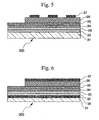
- FIG. 5 is a schematic sectional view illustrating one example of a functional element according to the present invention, wherein the functional element is a ferroelectric element (ferroelectric capacitor) 200.
- reference symbol 21 denotes a substrate consisting of silicon
- 22 denotes a first buffer layer
- 23 denotes a second buffer layer
- 24 denotes a first lower electrode layer
- 25 denotes a second lower electrode layer
- 26 denotes a ferroelectric layer
- 27 denotes an upper electrode layer, with 21 to 25 corresponding to the above described substrate 100 for electronic devices.
- FIG. 6 is a schematic sectional view illustrating another example of the functional element according to the present invention, wherein the functional element is a piezoelectric element (piezoelectric actuator) 300.
- reference symbol 31 denotes a substrate consisting of silicon
- 32 denotes a first buffer layer
- 33 denotes a second buffer layer
- 34 denotes a first lower electrode layer
- 35 denotes a second lower electrode layer
- 36 denotes a piezoelectric layer
- 37 denotes an upper electrode layer
- 38 denotes a thermal oxide film layer, with 31 to 35 including 38 corresponding to the above described substrate 100 for electronic devices.
- FIG. 1 is a schematic sectional view illustrating the configuration of the substrate for electronic devices according to this example
- FIG. 2 is a sectional view in each manufacturing step, when the substrate for electronic devices in FIG. 1 is manufactured.
- FIGS. 3A to 3E are photographs showing diffraction patterns obtained by observing the outermost surface in each manufacturing step, when the substrate for electronic devices in FIG. 1 is manufactured, using the RHEED method.
- FIGS. 4A and 4B are graphs illustrating results of studying the outermost surface of the substrate for electronic devices shown in FIG. 1 by an X-ray diffraction (XRD) method, wherein FIG. 4A represents the result of ⁇ -2 ⁇ scanning, and 4B represents the result of omega scanning of an SrRuO 3 (200) peak.
- XRD X-ray diffraction
- the substrate 100 for electronic devices comprises an Si substrate comprising a (100) plane, a first buffer layer 12 comprising a metal oxide having a fluorite structure epitaxially grown in a cubic (100) orientation on the Si substrate 11, a second buffer layer 13 comprising a metal oxide having a fluorite structure epitaxially grown in a cubic (100) orientation on the first buffer layer 12, a first oxide electrode layer 14 having a perovskite structure epitaxially grown in a tetragonal or orthorhombic (001) orientation on the second buffer layer 13, and a second oxide electrode layer 15 having a perovskite structure epitaxially grown in a cubic or pseudo-cubic (100) orientation on the first oxide electrode layer 14.
- a substrate in which the natural oxide film is not removed is used.
- YSZ is epitaxially grown in the cubic (100) orientation to a thickness of 5 nm.
- CeO 2 is epitaxially grown in the cubic (100) orientation to a thickness of 10 nm.
- YBa 2 Cu 3 O x is epitaxially grown in the tetragonal or orthorhombic (001) orientation.
- SrRuO 3 is epitaxially grown in the pseudo-cubic (100) orientation.
- the Si (100) substrate 11 is soaked in an organic solvent, and degreasing wash is conducted, using an ultrasonic cleansing machine.
- organic solvent for example, 1:1 liquid mixture of ethyl alcohol and acetone can be used, but it is not limited thereto.
- a step for removing the natural oxide film such as the RCA washing and washing with hydrofluoric acid, which are normal representative washing methods for Si substrates.
- the natural oxide film is formed on the surface of the Si (100) substrate 11.
- the substrate holder After loading the degreased Si (100) substrate 11 in a substrate holder, the substrate holder is introduced into a vacuum device in which the back pressure at room temperature is kept as 1 ⁇ 10 -8 Torr, and the vacuum device is heated to warm up to a temperature of 700°C at a rate of 10°C/min., using an infrared ray lamp.
- the natural oxide film layer 16 evaporates partly as SiO, and hence the pressure increases to 1.33 ⁇ 10 -4 Pa (1 ⁇ 10 -6 Torr) or higher, but at a temperature of 700°C, the pressure becomes constant at not higher than 6.66 ⁇ 10 -5 Pa (5 ⁇ 10 -7 Torr).
- pulsed radiation of a KrF excimer laser (wavelength: 248 nm) is shone onto the YSZ target surface arranged opposite to the Si (100) substrate 11, under conditions of an energy density of 2.5 J/cm 2 , a frequency of 10 Hz, and a pulse length of 10 ns, to generate a plasma plume consisting of Y, Zr and O on the target surface.
- This plasma plume is irradiated onto the Si (100) substrate 11 located at a position away from the target by 40 mm, for 10 minutes under conditions of a substrate temperature of 700°C, and a pressure during deposition of 6.66 ⁇ 10 -3 Pa (5 ⁇ 10 -5 Torr), so that the YSZ first buffer layer 12 is deposited to 5 nm ( FIG. 2B ).
- FIG. 3B a diffraction pattern has appeared in the RHEED pattern from the Si ⁇ 011> direction, and it is clearly seen that the epitaxial growth is achieved in an azimuthal relation of YSZ (100) / Si (100), YSZ ⁇ 011> // Si ⁇ 011>.
- the target composition is YSZ
- the substrate temperature is from 600°C to 800°C inclusive
- the back pressure during deposition is not higher than 6.66 ⁇ 10 -2 Pa (5 ⁇ 10 -4 Torr).
- the respective conditions are not limited thereto, so long as the oxide layer SiO 2 (natural oxide film) on the surface of the Si substrate 11 is reduced to Si, by irradiating a Zr gas or plasma onto the Si substrate 11 held at a temperature, a back pressure and an oxygen partial pressure such that the vapor pressure of SiO does not reach the saturated vapor pressure, and so long as YSZ can be grown epitaxially while removing Si by sublimating the Si formed by reduction as SiO.
- the laser energy density is not lower than 1 J/cm 2
- the laser frequency is not lower than 5 Hz
- the target-substrate distance is from 50 mm to 80 mm inclusive.
- the respective conditions are not limited thereto, so long as the deposition rate of YSZ is not lower than the growth rate (0.2 nm/min.) of the thermally oxidized SiO 2 film on the surface of the Si substrate, and YSZ can be grown epitaxially without forming the thermally oxidized SiO 2 film on the surface of the Si substrate 11.
- the YSZ first buffer layer 12 does not change, but oxygen is supplied to the interface between the Si (100) substrate 11 and the YSZ first buffer layer 12, to thereby form a thermal oxide film.
- ZrO 2 forms a solid solution as a cubic, then similar effects can be obtained when at least one of La, Ce, Pr, Nd, Pm, Sm, Eu, Gd, Tb, Dy, Ho, Er, Tm, Yb, Lu, Mg, Ca, Sr and Ba is added instead of Y.
- pulsed radiation of the KrF excimer laser is shone onto a CeO 2 target surface arranged opposite to the substrate, under conditions of an energy density of 2.5 J/cm 2 , a frequency of 10 Hz, and a pulse length of 10 ns, to generate a plasma plume consisting of Ce and O on the target surface.
- This plasma plume is irradiated onto the Si (100) substrate 11 located at a position away from the target by 40 mm, for 10 minutes under conditions of a substrate temperature of 700°C, and a pressure during deposition of 6.66 ⁇ 10 -3 Pa (5 ⁇ 10 -5 Torr), so that the CeO 2 second buffer layer 13 is deposited to 10 nm ( FIG. 2C ).
- the target composition is CeO 2
- the laser energy density is from 2 J/cm 2 to 3 J/cm 2 inclusive
- the laser frequency is not lower than 5 Hz and not higher than 15 Hz
- the target-substrate distance is from 30 mm to 50 mm inclusive
- the substrate temperature is from 650°C to 750°C inclusive
- the pressure during deposition is from 1 ⁇ 10 -5 Torr to 1 ⁇ 10- 4 Torr inclusive.
- the respective conditions are not limited thereto, so long as the epitaxial growth as CeO 2 is possible.
- CeO 2 forms a solid solution as a cubic
- similar effects can be obtained when at least one of Zr, La, Pr, Nd, Pm, Sm, Eu, Gd, Tb, Dy, Ho, Er, Tm, Yb, Lu, Mg, Ca, Sr and Ba is added.
- pulsed radiation of the KrF excimer laser is shone onto a YBa 2 Cu 3 O x target surface arranged opposite to the substrate, under conditions of an energy density of 2.5 J/cm 2 , a frequency of 5 Hz, and a pulse length of 10 ns, to generate a plasma plume consisting of Y, Ba, Cu and O on the target surface.
- This plasma plume is irradiated onto the Si substrate 11 located at a position away from the target by 40 mm, for 2 minutes under conditions of a substrate temperature of 600°C, and an oxygen partial pressure during deposition of 1.33 Pa (1 ⁇ 10 -2 Torr), so that the YBa 2 Cu 3 O x first oxide electrode layer 14 is deposited to 2 nm ( FIG. 2D ).
- the target composition is YBa 2 Cu 3 O x
- the laser energy density is from 2 J/cm 2 to 3 J/cm 2 inclusive
- the laser frequency is not lower than 2 Hz and not higher than 10 Hz
- the target-substrate distance is from 30 mm to 50 mm inclusive
- the substrate temperature is from 550°C to 650°C inclusive
- the pressure during deposition is from 1.33 ⁇ 10 -1 to 1.33 Pa (1 ⁇ 10 -3 Torr to 1 ⁇ 10 -1 Torr) inclusive.
- the respective conditions are not limited thereto, so long as the epitaxial growth as YBa 2 Cu 3 O 1 is possible.
- M 2 RuO 4 Ca, Sr or Ba
- RE 2 NiO 4 La, Ce, Pr, Nd, Pm, Sm, Eu, Gd, Tb, Dy, Ho, Er, Tm, Yb, Lu or Y
- pulsed radiation of the KrF excimer laser is shone onto an SrRuO 3 target surface arranged opposite to the substrate, under conditions of an energy density of 2.5 J/cm 2 , a frequency of 5 Hz, and a pulse length of 10 ns, to generate a plasma plume consisting of Sr, Ru and O on the target surface.
- This plasma plume is irradiated onto the Si substrate 11 located at a position away from the target by 40 mm, for 30 minutes under conditions of a substrate temperature of 600°C, and an oxygen partial pressure during deposition of 1.33 Pa (1 ⁇ 10 -2 Torr), so that the SrRuO 3 second oxide electrode layer 15 is deposited to 100 nm ( FIG. 2E ).
- the target composition is SrRuO 3
- the laser energy density is from 2 J/cm 2 to 3 J/cm 2 inclusive
- the laser frequency is not lower than 2 Hz and not higher than 10 Hz
- the target-substrate distance is from 30 mm to 50 mm inclusive
- the substrate temperature is from 550°C to 650°C inclusive
- the oxygen partial pressure during deposition is from 0.133 to 13.3 Pa ( 1 ⁇ 10 -3 Torr to 1 ⁇ 10 -1 Torr) inclusive.
- the respective conditions are not limited thereto, so long as the Sr and Ru plasma can reach the substrate at a constant ratio of 1:1, and the epitaxial growth as SrRuO 3 is possible.
- M Ca or Ba
- RE M)CrO 3 La, Ce, Pr, Nd, Pm, Sm, Eu, Gd, Tb, Dy, Ho, Er, Tm, Yb, Lu or Y
- M Ca, Sr, or Ba
- RE M)MnO 3 La, Ce, Pr, Nd, Pm, Sm, Eu, Gd, Tb, Dy, Ho, Er, Tm, Yb, Lu or Y
- M Ca, Sr, or Ba
- M Ca, Sr, or Ba
- RE, M)NiO 3 La, Ce, Pr, Nd, Pm, Sm, Eu, Gd, Tb, Dy, Ho, Er, Tm, Yb
- the XRD ⁇ -2 ⁇ scan of the thus obtained substrate 100 for electronic devices is shown in FIG. 4A , wherein peaks of pseudo-cubic SrRuO 3 (100) and SrRuO 3 (200) are clearly observed, together with the peaks of Si (200) and Si (400), which agrees with the observation result by the RHEED, indicating the (100) orientation.
- An ⁇ scan of the SrRuO 3 (200) peak is shown in FIG. 4B , by which it becomes clear that the full width at half maximum is 1.9 degrees, the crystallinity is excellent, and it is also useful as a foundation for epitaxial growth of a ferroelectric having the perovskite structure.
- any film-forming method such as an application method by spin coating, dip coating or ink jet printing, a chemical evaporation method such as MOCVD, and a physical vapor deposition method such as sputtering can be used instead of the laser ablation, to obtain similar effects.
- a perovskite substrate for electronic devices pseudo-cubically oriented in the (100) direction can be deposited on the Si substrate coated with a natural oxide film, and as a lower electrode for allowing oxides having the perovskite structure to grow epitaxially this enables realization of improvement in the characteristics of various kinds of electronic devices, as represented by the ferroelectric capacitor.
- the ferroelectric capacitor in which the substrate for electronic devices according to the present invention is used as the lower electrode whose schematic sectional view is shown in FIG. 5 , and the manufacturing method therefor will be described.
- the ferroelectric capacitor 200 comprises; an Si substrate 21 consisting of a (100) plane, a first buffer layer 22 comprising a metal oxide having a fluorite structure epitaxially grown in a cubic (100) orientation on the Si substrate 21, a second buffer layer 23 comprising a metal oxide having a fluorite structure epitaxially grown in a cubic (100) orientation on the first buffer layer 22, a first lower electrode layer 24 having a perovskite structure epitaxially grown in a tetragonal or orthorhombic (001) orientation on the second buffer layer 23, a second lower electrode layer 25 having a perovskite structure epitaxially grown in a cubic or pseudo-cubic (100) orientation on the first lower electrode layer 24, a ferroelectric layer 26 having a perovskite structure epitaxially grown in a tetragonal (001) orientation on the second lower electrode layer 25, and an upper electrode layer 27 formed on the ferroelectric layer 26.
- a substrate in which the natural oxide film is not removed is used.
- YSZ is epitaxially grown in the cubic (100) orientation to a thickness of 5 nm.
- CeO 2 is epitaxially grown in the cubic (100) orientation to a thickness of 10 nm.
- YBa 2 Cu 3 O x is epitaxially grown in the tetragonal or orthorhombic (001 ) orientation, to a thickness of 2 nm.
- SrRuO 3 is epitaxially grown in the pseudo-cubic (100) orientation, to a thickness of 100 nm.
- PbZr 0.40 Ti 0.60 O 3 is epitaxially grown in the tetragonal (001) orientation. Pt is used for the upper electrode layer 27.
- the washing step of the Si (100) substrate 21, the heating and warm-up step, the deposition step of the first buffer layer 22, the deposition step of the second buffer layer 23, the deposition step of the first lower electrode layer 24, and the deposition step of the second lower electrode layer 25 are the same as in the manufacturing method for the substrate 100 for electronic devices shown in Example 1.
- pulsed radiation of the KrF excimer laser is shone onto a PbZr 0.40 Ti 0.60 O 3 target surface arranged opposite to the substrate, under conditions of an energy density of 2.0 J/cm 2 , a frequency of 5 Hz, and a pulse length of 10 ns, to generate a plasma plume consisting of Pb, Zr, Ti and O on the target surface.
- This plasma plume is irradiated onto the Si substrate 21 located at a position away from the target by 40 mm, for 30 minutes under conditions of a substrate temperature of 600°C, and an oxygen partial pressure during deposition of 1.33 Pa (1 ⁇ 10 -2 Torr), so that the PbZr 0.40 Ti 0 .60 O 3 ferroelectric layer 24 is deposited to 150 nm.
- the target composition is PZT
- the laser energy density is from 1.0 J/cm 2 to 3.0 J/cm 2 inclusive
- the laser frequency is not lower than 2 Hz and not higher than 10 Hz
- the target-substrate distance is from 30 mm to 50 mm inclusive
- the substrate temperature is from 550°C to 650°C inclusive
- the oxygen partial pressure during deposition is from 0.133 to 13.3 Pa (1 ⁇ 10 -3 Torr to 1 ⁇ 10 -1 Torr) inclusive.
- the respective conditions are not limited thereto, so long as the epitaxial growth as PZT is possible.
- ferroelectrics having the perovskite structure as represented by BaTiO 3 , KNbO 3 , and BiFeO 3 , and solid solutions of these ferroelectrics and various kinds of paraelectrics, instead of PZT.
- etching is performed by using a known method such as photolithography, and the second lower electrode layer 25 is taken out, and a Pt upper electrode layer 27 is deposited by a known method such as sputtering, while using a mask pattern. Similar effects can be obtained by using other electrode materials generally used for electrodes, such as Ir, instead of Pt.
- the thus obtained ferroelectric capacitor 200 has an orientation relation of Pt/PZT (001) / SrRuO 3 (100) /YBa 2 Cu 3 O x (001) / CeO 2 (100) / YSZ (100) / Si (100), and an azimuthal relation of PZT ⁇ 010> // SrRuO 3 ⁇ 010> // YBa 2 Cu 3 O x ⁇ 100> // CeO 2 ⁇ 011> // YSZ ⁇ 011> // Si ⁇ 011> within a plane.
- any film-forming method such as an application method by spin coating, dip coating or ink jet printing, a chemical evaporation method such as MOCVD, and a physical vapor deposition method such as sputtering can be used instead of the laser ablation, to obtain similar effects.
- the tetragonal (001) epitaxial growth of the ferroelectric layer having the perovskite structure can be achieved, thereby realizing a ferroelectric memory having a ferroelectric capacitor excellent in the polarization characteristic.
- the piezoelectric actuator 300 comprises; an Si substrate 31 consisting of a (100) plane, a first buffer layer 32 comprising a metal oxide having a fluorite structure epitaxially grown in a cubic (100) orientation on the Si substrate 31, a second buffer layer 33 comprising a metal oxide having a fluorite structure epitaxially grown in a cubic (100) orientation on the first buffer layer 32, a first lower electrode layer 34 having a perovskite structure epitaxially grown in a tetragonal or orthorhombic (001) orientation on the second buffer layer 33, a second lower electrode layer 35 having a perovskite structure epitaxially grown in a cubic or pseudo-cubic (100) orientation on the first lower electrode layer 34, a piezoelectric layer 36 having a perovskite structure epitaxially grown in a rhombohedral (100) orientation on the second lower electrode layer 35, and an upper electrode layer 37 formed on the piezoelectric layer 36.
- SiO 2 thermal oxide film layer 38 which serves as a resilient board in the actuator, together with the Si substrate 31.
- Si substrate 31 a substrate in which the natural oxide film is not removed was used.
- YSZ is epitaxially grown in the cubic (100) orientation to a thickness of 5 nm.
- CeO 2 is epitaxially grown in the cubic (100) orientation to a thickness of 10 nm.
- YBa 2 Cu 3 O x is epitaxially grown in the tetragonal or orthorhombic (001) orientation, to a thickness of 2 nm.
- SrRuO 3 is epitaxially grown in the pseudo-cubic (100) orientation, to a thickness of 100 nm.
- PbZr 0.55 Ti 0.45 O 3 is epitaxially grown in the rhombohedral (100) orientation. Ir is used for the upper electrode layer 37.
- the washing step of the Si (100) substrate 31, the heating and warm-up step, the deposition step of the first buffer layer 32, the deposition step of the second buffer layer 33, the deposition step of the first lower electrode layer 34, and the deposition step of the second lower electrode layer 35 are the same as in the manufacturing method for the substrate 100 for electronic devices shown in Example 1.
- pulsed radiation of the KrF excimer laser is shone onto a PbZr 0.55 Ti 0.45 O 3 target surface arranged opposite to the substrate, under conditions of an energy density of 2.0 J/cm 2 , a frequency of 10 Hz, and a pulse length of 10 ns, to generate a plasma plume consisting of Pb, Zr, Ti and O on the target surface.
- This plasma plume is irradiated onto the Si substrate 31 located at a position away from the target by 40 mm, for 90 minutes under conditions of a substrate temperature of 600°C, and an oxygen partial pressure during deposition of 1.33 Pa (1 ⁇ 10 -2 Torr), so that the PbZr 0.55 Ti 0.45 O 3 piezoelectric layer 36 is deposited to 900 nm.
- oxygen is supplied to the interface between the Si substrate 31 and the YSZ first buffer layer 32 to form an SiO 2 thermal oxide film layer 38 to a thickness of 500 nm.
- the target composition is PZT
- the laser energy density is from 1.0 J/cm 2 to 3.0 J/cm 2 inclusive
- the laser frequency is not lower than 5 Hz and not higher than 15 Hz
- the target-substrate distance is from 30 mm to 50 mm inclusive
- the substrate temperature is from 550°C to 650°C inclusive
- the oxygen partial pressure during deposition is from 0.133 to 13.3 Pa (1 ⁇ 10 -3 Torr to 1 ⁇ 10 -1 Torr) inclusive.
- the respective conditions are not limited thereto, so long as the Pb, Zr and Ti plasma can reach the substrate at a desired constant ratio, and the epitaxial growth as PZT is possible.
- ferroelectrics having the perovskite structure as represented by Pb(Mb, Nb)O 3 , Pb(Zn, Nb)O 3 , BaTiO 3 , KNbO 3 , and BiFeO 3 , and solid solutions of these ferroelectrics and various kinds of paraelectrics, instead of PZT.
- etching is performed by using a known method such as photolithography, and the lower electrode layer 35 is taken out, and an Ir upper electrode layer 37 is deposited by a known method such as sputtering, while using a mask pattern. Similar effects can be obtained by using other electrode materials generally used for electrodes, such as Pt, instead of Ir.
- the thus obtained piezoelectric capacitor 300 has an orientation relation of Ir/PZT (100) / SrRuO 3 (100) / YBa 2 Cu 3 O x (001 ) / CeO 2 (100) / YSZ (100) / Si (100), and an azimuthal relation of PZT ⁇ 010> // SrRuO 3 ⁇ 010> // YBa 2 Cu 3 O x ⁇ 100> // CeO 2 ⁇ 011> // YSZ ⁇ 011> // Si ⁇ 011>.
- This can be considered to be an effect of an engineered domain in which the piezoelectric effect increases when angles between a polarizing axis of each domain in the piezoelectric layer and the electric field are all equal and not 0 degrees.
- any film-forming method such as an application method by spin coating, dip coating or ink jet printing, a chemical evaporation method such as MOCVD, and a physical vapor deposition method such as sputtering can be used instead of the laser ablation, to obtain similar effects.
- the piezoelectric actuator in which the substrate for electronic devices having the above configuration is used for the lower electrode, it has been confirmed that the rhombohedral (100) epitaxial growth of the piezoelectric layer having the perovskite structure can be achieved, thereby enabling improvement in the field distortion characteristic of the piezoelectric element.
Landscapes
- Engineering & Computer Science (AREA)
- Manufacturing & Machinery (AREA)
- Semiconductor Memories (AREA)
- Crystals, And After-Treatments Of Crystals (AREA)
- Chemical Vapour Deposition (AREA)
- Recrystallisation Techniques (AREA)
Claims (23)
- Substrat (100) für elektronische Vorrichtungen, umfassend: ein Substrat (11), das aus Silicium besteht und eine filmbildende Oberfläche, und eine erste Pufferschicht (12), eine zweite Pufferschicht (13), eine erste Oxidelektrodenschicht (14) und eine zweite Oxidelektrodenschicht (15) aufweist, die epitaktisch gewachsen und in dieser Reihenfolge auf die filmbildende Oberfläche des Substrats (11) laminiert werden, wobei
die erste Pufferschicht (12) ein erstes Metalloxid ist, das eine Fluoritstruktur aufweist,
die zweite Pufferschicht (13) ein zweites Metalloxid ist, das eine Fluoritstruktur aufweist,
die erste Oxidelektrodenschicht (14) ein drittes Metalloxid ist, das eine geschichtete Perowskitstruktur aufweist, und
die zweite Oxidelektrodenschicht (15) ein viertes Metalloxid ist, das eine einfache Perowskitstruktur aufweist. - Substrat für elektronische Vorrichtungen nach Anspruch 1, wobei die Orientierung der filmbildenden Oberfläche (100), (110) oder (111) ist.
- Substrat für elektronische Vorrichtungen nach Anspruch 1, wobei in der filmbildenen Oberfläche kein Beugungsmuster in einem Beugungsbild mittels RHEED-Verfahren beobachtet wird, bevor die erste Pufferschicht gebildet wird.
- Substrate für elektronische Vorrichtungen nach Anspruch 1, wobei das erste Metalloxid eine feste Lösung ist, ausgedrückt als Zr1-xMαxOy (0 < x < 1, 1,5 < y < 2), die durch Substituieren eines Teils von Zr, das ein Elementarbestandteil von Zirconiumoxid ist, mit einem Metallelement Mα erhalten wird, wobei Mα einen Elementtyp angibt, ausgewählt aus La, Ce, Pr, Nd, Pm, Sm, Eu, Gd, Tb, Dy, Ho, Er, Tm, Yb, Lu, Y, Mg, Ca, Sr und Ba, und das erste Metalloxid in der (100) - Richtung kubisch orientiert ist.
- Substrate für elektronische Vorrichtungen nach Anspruch 1, wobei das zweite Metalloxid Ceroxid oder eine feste Lösung ist, ausgedrückt als Ce1-xMβxOy (0 < x < 1, 1,5 < y < 2), die durch Substituieren eines Teils von Ce, das ein Elementarbestandteil von Ceroxid ist, mit einem Metallelement Mβ erhalten wird, wobei Mβ einen Elementtyp angibt, ausgewählt aus Zr, La, Pr, Nd, Pm, Sm, Eu, Gd, Tb, Dy, Ho, Er, Tm, Yb, Lu, Y, Mg, Ca, Sr und Ba, und das zweite Metalloxid in der (100)-Richtung kubisch orientiert ist.
- Substrat für elektronische Vorrichtungen nach Anspruch 1, wobei das dritte Metalloxid eine feste Lösung ist, die ein Metallelement Mγ oder RE als einen Elementarbestandteil enthält, und als MγRuO4, RE2NiO4, oder REBa2Cu3Ox ausgedrückt wird, wobei Mγ einen Elementtyp angibt, ausgewählt aus Ca, Sr und Ba, und RE einen Elementtyp angibt, ausgewählt aus La, Ce, Pr, Nd, Pm, Sm, Eu, Gd, Tb, Dy, Ho, Er, Tm, Yb, Lu und Y, und das dritte Metalloxid in der (001)-Richtung tetragonal oder orthorhombisch orientiert ist.
- Substrat für elektronische Vorrichtungen nach Anspruch 1, wobei das vierte Metalloxid eine feste Lösung ist, die ein Metallelement Mγ oder RE als einen Elementarbestandteil enthält, und als Mγ RuO3, (RE, Mγ) CrO3, (RE, Mγ) MnO3, (RE, Mγ) CoO3 oder (RE, Mγ) NiO3 ausgedrückt wird, wobei Mγ einen Elementtyp angibt, ausgewählt aus Ca, Sr und Ba, und RE einen Elementtyp angibt, ausgewählt aus La, Ce, Pr, Nd, Pm, Sm, Eu, Gd, Tb, Dy, Ho, Er, Tm, Yb, Lu und Y, und das dritte Metalloxid in der (001)-Richtung kubisch oder pseudokubisch orientiert ist.
- Verfahren zur Herstellung eines Substrats für elektronische Vorrichtungen, umfassend:einen Vorbehandlungsschritt zum Waschen eines Substrats (11), das aus Silicium besteht und eine filmbildende Oberfläche aufweist;einen ersten Filmbildungsschritt, in dem das Substrat, nachdem es dem Vorbehandlungsschritt unterzogen wurde, in einem Filmbildungsbehälter unter einer Atmosphäre mit reduziertem Druck angeordnet wird, und ein vorbestimmtes Gas oder Plasma auf die filmbildende Oberfläche des Substrats gestrahlt wird, um eine erste Pufferschicht (12) epitaktisch zu wachsen, die ein erstes Metalloxid umfasst, das eine Fluoritstruktur aufweist;einen zweiten Filmbildungsschritt, in dem ein vorbestimmtes Gas oder Plasma auf die Oberfläche der ersten Pufferschicht gestrahlt wird, um eine zweite Pufferschicht (13) epitaktisch zu wachsen, die ein zweites Metalloxid umfasst, das eine Fluoritstruktur aufweist;einen dritten Filmbildungsschritt, in dem ein vorbestimmtes Gas oder Plasma auf die Oberfläche der zweiten Pufferschicht gestrahlt wird, um eine erste Oxidelektronenschicht (14) epitaktisch zu wachsen, die ein drittes Metalloxid umfasst, das eine geschichtete Perowskitstruktur aufweist;einen vierten Filmbildungsschritt, in dem ein vorbestimmtes Gas oder Plasma auf die Oberfläche der ersten Oxidelektrodenschicht gestrahlt wird, um eine zweite Oxidelektrodenschicht (15) epitaktisch zu wachsen, die ein viertes Metalloxid umfasst, das eine einfache Fluoritstruktur aufweist.
- Verfahren zur Herstellung eines Substrats für elektronische Vorrichtungen nach Anspruch 8, wobei in dem ersten Filmbildungsschritt ein Gas oder Plasma eines Elementarbestandteils der ersten Pufferschicht auf die filmbildende Oberfläche des Substrats gestrahlt wird, das unter einer Temperatur, einem Rückdruck und einem Sauerstoffpartialdruck gehalten wird, so dass der Dampfdruck von SiO den Sättigungsdampfdruck nicht erreicht.
- Verfahren zur Herstellung eines Substrats für elektronische Vorrichtungen nach Anspruch 9, wobei in dem ersten Filmbildungsschritt ein SiO2-Film, der eine Oxidschicht bildet, die auf der filmbildenden Oberfläche des Substrats vorhanden ist, zu Si reduziert wird, und eine erste Metalloxidschicht, die die erste Pufferschicht bildet, abgelagert wird, während das Si sublimiert und entfernt wird, das sich bei der Reduktion als SiO gebildet hat.
- Verfahren zur Herstellung eines Substrats für elektronische Vorrichtungen nach Anspruch 9, wobei in dem ersten Filmbildungsschritt, wenn die erste Pufferschicht gebildet wird, die Temperatur des Substrats 800 °C oder höher ist, der Rückdruck in der filmbildenden Atmosphäre nicht niedriger als 1,33 x 10⁻⁴ Pa (1 x 10⁻⁶ Torr) ist, und der Sauerstoffpartialdruck in der filmbildenden Atmosphäre nicht niedriger als 6,66 x 10⁻⁴ Pa (5 x 10⁻⁶ Torr) ist.
- Verfahren zur Herstellung eines Substrats für elektronische Vorrichtungen nach Anspruch 11, wobei in dem ersten Filmbildungsschritt, wenn die erste Pufferschicht gebildet wird, die Temperatur des Substrats zwischen einschließlich 600 °C und 800 °C liegt, der Rückdruck in der filmbildenden Atmosphäre zwischen einschließlich 1,33 x 10⁻⁴ Pa und 6,66 x 10⁻⁴ Pa (1 x 10⁻⁶ Torr und 5 x 10⁻⁶ Torr) liegt, und der Sauerstoffpartialdruck in der filmbildenden Atmosphäre zwischen einschließlich 6,66 x 10⁻⁴ Pa und 6,66 x 10⁻² Pa (5 x 10⁻⁶ Torr und 5 x 10⁻⁴ Torr) liegt.
- Verfahren zur Herstellung eines Substrats für elektronische Vorrichtungen nach Anspruch 9, wobei in dem ersten Filmbildungsschritt die erste Pufferschicht mit einer Ablagerungsrate auf der filmbildenen Oberfläche des Substrats gebildet wird, die nicht niedriger ist als eine Wachstumsrate eines thermisch oxidierten SiO2-Films.
- Verfahren zur Herstellung eines Substrats für elektronische Vorrichtungen nach Anspruch 13, wobei in dem ersten filmbildenden Schritt die erste Pufferschicht auf der filmbildenden Oberfläche nach dem Entfernen des SiO2-Films epitaktisch gewachsen wird, ohne einen thermisch oxidierten SiO2-Film zu bilden.
- Verfahren zur Herstellung eines Substrats für elektronische Vorrichtungen nach Anspruch 13, wobei in dem ersten Filmbildungsschritt die Ablagerungsrate der ersten Pufferschicht nicht niedriger als 0,2 nm/Min. ist.
- Verfahren zur Herstellung eines Substrats für elektronische Vorrichtungen nach Anspruch 8, wobei die vorbestimmten Gase oder Plasmen Elemente umfassen, die Metalloxide bilden, die in jedem Schritt des ersten Filmbildungsschritts, des zweiten Filmbildungsschritts, des dritten Filmbildungsschritts und des vierten Filmbildungsschritts zu bilden sind.
- Verfahren zur Herstellung eines Substrats für elektronische Vorrichtungen nach Anspruch 8, wobei das vorbestimmte Gas oder Plasma erzeugt wird, indem ein Laserstrahl auf ein Grundmetall gestrahlt wird, das gegenüber der filmbildenden Oberfläche des Substrats angeordnet ist.
- Verfahren zur Herstellung eines Substrats für elektronische Vorrichtungen nach Anspruch 8, wobei in dem Vorbehandlungsschritt die filmbildende Oberfläche des Substrats als Oberfläche fertig gestellt wird, auf der eine Oxidschicht nicht als rekonstruierte Oberfläche oder wasserstoffterminierte Oberfläche vorhanden ist.
- Elektronische Vorrichtung, die ein Funktionselement ist, umfassend ein Substrat für elektronische Vorrichtungen nach einem der Ansprüche 1 bis 7.
- Elektronische Vorrichtung nach Anspruch 19, wobei das Funktionselement ein Kondensator ist.
- Elektronische Vorrichtung nach Anspruch 19, wobei das Funktionselement ein ferroelektrisches Element ist.
- Elektronische Vorrichtung nach Anspruch 19, wobei das Funktionselement ein Kantilever ist.
- Elektronische Vorrichtung nach Anspruch 19, wobei das Funktionselement ein piezoelektrisches Element ist.
Applications Claiming Priority (4)
| Application Number | Priority Date | Filing Date | Title |
|---|---|---|---|
| JP2002259960 | 2002-09-05 | ||
| JP2002259960 | 2002-09-05 | ||
| JP2003194243 | 2003-07-09 | ||
| JP2003194243A JP4457587B2 (ja) | 2002-09-05 | 2003-07-09 | 電子デバイス用基体の製造方法及び電子デバイスの製造方法 |
Publications (3)
| Publication Number | Publication Date |
|---|---|
| EP1396877A2 EP1396877A2 (de) | 2004-03-10 |
| EP1396877A3 EP1396877A3 (de) | 2005-02-02 |
| EP1396877B1 true EP1396877B1 (de) | 2008-11-26 |
Family
ID=31719912
Family Applications (1)
| Application Number | Title | Priority Date | Filing Date |
|---|---|---|---|
| EP20030255438 Expired - Lifetime EP1396877B1 (de) | 2002-09-05 | 2003-09-01 | Träger für elektronische Vorrichtungen, dessen Verfahren zur Herstellung, und elektronische Vorrichtung |
Country Status (5)
| Country | Link |
|---|---|
| US (2) | US6960539B2 (de) |
| EP (1) | EP1396877B1 (de) |
| JP (1) | JP4457587B2 (de) |
| CN (1) | CN1260774C (de) |
| DE (1) | DE60324868D1 (de) |
Families Citing this family (39)
| Publication number | Priority date | Publication date | Assignee | Title |
|---|---|---|---|---|
| JP4228569B2 (ja) * | 2001-11-28 | 2009-02-25 | セイコーエプソン株式会社 | 電子デバイス用基板の製造方法及び電子デバイスの製造方法 |
| US7009235B2 (en) * | 2003-11-10 | 2006-03-07 | Unity Semiconductor Corporation | Conductive memory stack with non-uniform width |
| JP2005150694A (ja) * | 2003-10-23 | 2005-06-09 | Seiko Epson Corp | 圧電体膜、圧電素子、圧電アクチュエーター、圧電ポンプ、インクジェット式記録ヘッド、インクジェットプリンター、表面弾性波素子、薄膜圧電共振子、周波数フィルタ、発振器、電子回路、および電子機器 |
| JP4717344B2 (ja) * | 2003-12-10 | 2011-07-06 | キヤノン株式会社 | 誘電体薄膜素子、圧電アクチュエータおよび液体吐出ヘッド |
| US7262544B2 (en) * | 2004-01-09 | 2007-08-28 | Canon Kabushiki Kaisha | Dielectric element, piezoelectric element, ink jet head and method for producing the same head |
| US7265483B2 (en) * | 2004-03-29 | 2007-09-04 | Canon Kabushiki Kaisha | Dielectric member, piezoelectric member, ink jet head, ink jet recording apparatus and producing method for ink jet recording apparatus |
| JP4865249B2 (ja) * | 2004-08-31 | 2012-02-01 | 株式会社リコー | スパッタリングターゲットとその製造方法、及び光記録媒体 |
| JP4431891B2 (ja) | 2004-12-28 | 2010-03-17 | セイコーエプソン株式会社 | 圧電素子、圧電アクチュエーター、圧電ポンプ、インクジェット式記録ヘッド、インクジェットプリンター、表面弾性波素子、薄膜圧電共振子、周波数フィルタ、発振器、電子回路、および電子機器 |
| JP4237184B2 (ja) * | 2005-03-31 | 2009-03-11 | エルピーダメモリ株式会社 | 半導体装置の製造方法 |
| CN100483700C (zh) * | 2005-06-27 | 2009-04-29 | 电子科技大学 | 导电氧化物电极材料制备方法 |
| JP5158299B2 (ja) * | 2005-08-05 | 2013-03-06 | セイコーエプソン株式会社 | 圧電素子、アクチュエータ装置、液体噴射ヘッド、液体噴射装置及び圧電素子の製造方法 |
| JP4753027B2 (ja) * | 2006-04-12 | 2011-08-17 | セイコーエプソン株式会社 | インクジェット式記録ヘッドおよびインクジェットプリンタ |
| JP4753028B2 (ja) * | 2006-04-12 | 2011-08-17 | セイコーエプソン株式会社 | インクジェット式記録ヘッドおよびインクジェットプリンタ |
| TWI381060B (zh) * | 2008-08-12 | 2013-01-01 | Univ Tatung | High frequency surface acoustic wave elements and their substrates |
| KR20100111117A (ko) * | 2009-04-06 | 2010-10-14 | 삼성전기주식회사 | 박막소자의 제조방법 및 이로부터 제조된 박막소자 |
| WO2010151844A2 (en) * | 2009-06-25 | 2010-12-29 | Georgia Tech Research Corporation | Metal oxide structures, devices, & fabrication methods |
| US9853325B2 (en) | 2011-06-29 | 2017-12-26 | Space Charge, LLC | Rugged, gel-free, lithium-free, high energy density solid-state electrochemical energy storage devices |
| US11527774B2 (en) | 2011-06-29 | 2022-12-13 | Space Charge, LLC | Electrochemical energy storage devices |
| US10601074B2 (en) | 2011-06-29 | 2020-03-24 | Space Charge, LLC | Rugged, gel-free, lithium-free, high energy density solid-state electrochemical energy storage devices |
| US11996517B2 (en) | 2011-06-29 | 2024-05-28 | Space Charge, LLC | Electrochemical energy storage devices |
| US10658705B2 (en) | 2018-03-07 | 2020-05-19 | Space Charge, LLC | Thin-film solid-state energy storage devices |
| TWI421328B (zh) | 2011-09-06 | 2014-01-01 | Ind Tech Res Inst | 螢光材料與白光發光裝置 |
| CN102912332B (zh) * | 2012-09-03 | 2014-12-03 | 西南交通大学 | 一种化学溶液沉积法制备RexCe1-xOy/M2Zr2O7双层缓冲层的方法 |
| JP2014116443A (ja) * | 2012-12-10 | 2014-06-26 | Panasonic Corp | 圧電体素子および圧電体素子の製造方法 |
| JP6201128B2 (ja) * | 2013-03-01 | 2017-09-27 | 株式会社ユーテック | 配向基板、配向膜基板の製造方法、スパッタリング装置及びマルチチャンバー装置 |
| JP6212741B2 (ja) * | 2013-03-01 | 2017-10-18 | 株式会社ユーテック | 配向基板 |
| DE112014003430B4 (de) * | 2013-07-25 | 2025-10-16 | Ngk Ceramic Device Co.,Ltd., | Kompositsubstrat und Verfahren zum Herstellen desselben |
| JP6956716B2 (ja) * | 2015-11-13 | 2021-11-02 | アイキューイー ピーエルシーIQE plc | 希土類酸化物およびエピタキシャル窒化アルミニウムを用いて加工されるrfフィルタのための層構造 |
| US10186595B2 (en) * | 2016-08-05 | 2019-01-22 | Northwestern University | Noncentrosymmetric metal electrodes for ferroic devices |
| US11495670B2 (en) | 2016-09-22 | 2022-11-08 | Iqe Plc | Integrated epitaxial metal electrodes |
| JP7005604B2 (ja) | 2016-09-22 | 2022-01-21 | アイキューイー ピーエルシー | 統合されたエピタキシャル金属電極 |
| US10418457B2 (en) | 2016-09-22 | 2019-09-17 | Iqe Plc | Metal electrode with tunable work functions |
| JP6497712B2 (ja) * | 2017-02-27 | 2019-04-10 | アドバンストマテリアルテクノロジーズ株式会社 | 配向基板、配向膜基板の製造方法、スパッタリング装置及びマルチチャンバー装置 |
| JP6497713B2 (ja) * | 2017-03-14 | 2019-04-10 | アドバンストマテリアルテクノロジーズ株式会社 | 配向基板、配向膜基板の製造方法、スパッタリング装置及びマルチチャンバー装置 |
| JP6481138B2 (ja) * | 2017-04-28 | 2019-03-13 | アドバンストマテリアルテクノロジーズ株式会社 | 配向膜基板の製造方法、スパッタリング装置及びマルチチャンバー装置 |
| US12052922B2 (en) * | 2020-03-26 | 2024-07-30 | Tdk Corporation | Piezoelectric thin film, piezoelectric thin film element and piezoelectric transducer |
| US11581335B2 (en) * | 2020-06-23 | 2023-02-14 | Taiwan Semiconductor Manufacturing Company Limited | Ferroelectric tunnel junction devices with metal-FE interface layer and methods for forming the same |
| CN112670087A (zh) * | 2020-12-09 | 2021-04-16 | 南京邮电大学 | 一种应用于铁电储存器中使用的铁电薄膜电容 |
| KR20230099536A (ko) | 2021-12-27 | 2023-07-04 | 삼성전자주식회사 | 배선 구조체 및 이를 포함하는 장치 |
Citations (1)
| Publication number | Priority date | Publication date | Assignee | Title |
|---|---|---|---|---|
| EP1505663A1 (de) * | 2002-05-15 | 2005-02-09 | Seiko Epson Corporation | Piezoelektrisches stellglied und flüssigkeits-jet-kopf |
Family Cites Families (32)
| Publication number | Priority date | Publication date | Assignee | Title |
|---|---|---|---|---|
| US5215631A (en) * | 1982-06-25 | 1993-06-01 | Cel Systems Corporation | Electrolytic preparation of tin, other metals, alloys and compounds |
| US5358925A (en) | 1990-04-18 | 1994-10-25 | Board Of Trustees Of The Leland Stanford Junior University | Silicon substrate having YSZ epitaxial barrier layer and an epitaxial superconducting layer |
| US5173474A (en) | 1990-04-18 | 1992-12-22 | Xerox Corporation | Silicon substrate having an epitaxial superconducting layer thereon and method of making same |
| JPH04214097A (ja) | 1990-12-13 | 1992-08-05 | Sumitomo Electric Ind Ltd | 超電導薄膜の作製方法 |
| US5085731A (en) * | 1991-02-04 | 1992-02-04 | Air Products And Chemicals, Inc. | Volatile liquid precursors for the chemical vapor deposition of copper |
| US5270298A (en) | 1992-03-05 | 1993-12-14 | Bell Communications Research, Inc. | Cubic metal oxide thin film epitaxially grown on silicon |
| US5155658A (en) | 1992-03-05 | 1992-10-13 | Bell Communications Research, Inc. | Crystallographically aligned ferroelectric films usable in memories and method of crystallographically aligning perovskite films |
| JP3222569B2 (ja) | 1992-09-11 | 2001-10-29 | 旭化成株式会社 | 半導体記憶素子 |
| JP3223233B2 (ja) | 1994-08-17 | 2001-10-29 | ティーディーケイ株式会社 | 酸化物薄膜、電子デバイス用基板および酸化物薄膜の形成方法 |
| US5828080A (en) | 1994-08-17 | 1998-10-27 | Tdk Corporation | Oxide thin film, electronic device substrate and electronic device |
| JP3346939B2 (ja) | 1995-03-15 | 2002-11-18 | ティーディーケイ株式会社 | Si基板およびその表面処理方法 |
| JPH08264524A (ja) | 1995-03-27 | 1996-10-11 | Japan Energy Corp | 多層半導体基板及びその製造方法 |
| JP3310881B2 (ja) | 1995-08-04 | 2002-08-05 | ティーディーケイ株式会社 | 積層薄膜、電子デバイス用基板、電子デバイスおよび積層薄膜の製造方法 |
| US5753934A (en) | 1995-08-04 | 1998-05-19 | Tok Corporation | Multilayer thin film, substrate for electronic device, electronic device, and preparation of multilayer oxide thin film |
| JP3562120B2 (ja) | 1996-03-29 | 2004-09-08 | 日産自動車株式会社 | 安定化ジルコニア薄膜と単結晶シリコン基体との複合構造体およびその製造方法 |
| JP3193302B2 (ja) | 1996-06-26 | 2001-07-30 | ティーディーケイ株式会社 | 膜構造体、電子デバイス、記録媒体および強誘電体薄膜の製造方法 |
| JP3684709B2 (ja) | 1996-10-03 | 2005-08-17 | 日産自動車株式会社 | 結晶性酸化物誘電体薄膜と単結晶シリコン基体との複合構造体およびそれを用いた電子素子およびそれらの製造方法 |
| TW347570B (en) * | 1996-12-24 | 1998-12-11 | Toshiba Co Ltd | Semiconductor device and method for manufacturing the same |
| JPH10265948A (ja) * | 1997-03-25 | 1998-10-06 | Rohm Co Ltd | 半導体装置用基板およびその製法 |
| US6139905A (en) * | 1997-04-11 | 2000-10-31 | Applied Materials, Inc. | Integrated CVD/PVD Al planarization using ultra-thin nucleation layers |
| JP3472087B2 (ja) | 1997-06-30 | 2003-12-02 | Tdk株式会社 | 膜構造体、電子デバイス、記録媒体および酸化物導電性薄膜の製造方法 |
| JP3813740B2 (ja) | 1997-07-11 | 2006-08-23 | Tdk株式会社 | 電子デバイス用基板 |
| JP4036544B2 (ja) | 1998-09-22 | 2008-01-23 | Tdk株式会社 | 電圧制御発振器 |
| JP3470068B2 (ja) | 1999-09-01 | 2003-11-25 | 松下電器産業株式会社 | 誘電体膜の形成方法 |
| JP4327942B2 (ja) | 1999-05-20 | 2009-09-09 | Tdk株式会社 | 薄膜圧電素子 |
| US6258223B1 (en) * | 1999-07-09 | 2001-07-10 | Applied Materials, Inc. | In-situ electroless copper seed layer enhancement in an electroplating system |
| JP2001122698A (ja) | 1999-10-26 | 2001-05-08 | Seiko Epson Corp | 酸化物電極薄膜 |
| US20010033020A1 (en) * | 2000-03-24 | 2001-10-25 | Stierman Roger J. | Structure and method for bond pads of copper-metallized integrated circuits |
| EP1139413B1 (de) * | 2000-03-24 | 2005-03-16 | Texas Instruments Incorporated | Verfahren zum Drahtbonden |
| US6921722B2 (en) * | 2000-05-30 | 2005-07-26 | Ebara Corporation | Coating, modification and etching of substrate surface with particle beam irradiation of the same |
| JP3796394B2 (ja) | 2000-06-21 | 2006-07-12 | キヤノン株式会社 | 圧電素子の製造方法および液体噴射記録ヘッドの製造方法 |
| US6376353B1 (en) * | 2000-07-03 | 2002-04-23 | Chartered Semiconductor Manufacturing Ltd. | Aluminum and copper bimetallic bond pad scheme for copper damascene interconnects |
-
2003
- 2003-07-09 JP JP2003194243A patent/JP4457587B2/ja not_active Expired - Fee Related
- 2003-08-21 US US10/644,989 patent/US6960539B2/en not_active Expired - Fee Related
- 2003-09-01 EP EP20030255438 patent/EP1396877B1/de not_active Expired - Lifetime
- 2003-09-01 DE DE60324868T patent/DE60324868D1/de not_active Expired - Lifetime
- 2003-09-03 CN CNB031565190A patent/CN1260774C/zh not_active Expired - Fee Related
-
2005
- 2005-03-31 US US11/094,665 patent/US20050167715A1/en not_active Abandoned
Patent Citations (1)
| Publication number | Priority date | Publication date | Assignee | Title |
|---|---|---|---|---|
| EP1505663A1 (de) * | 2002-05-15 | 2005-02-09 | Seiko Epson Corporation | Piezoelektrisches stellglied und flüssigkeits-jet-kopf |
Also Published As
| Publication number | Publication date |
|---|---|
| US20050167715A1 (en) | 2005-08-04 |
| CN1260774C (zh) | 2006-06-21 |
| EP1396877A3 (de) | 2005-02-02 |
| EP1396877A2 (de) | 2004-03-10 |
| CN1487564A (zh) | 2004-04-07 |
| DE60324868D1 (de) | 2009-01-08 |
| US20040053460A1 (en) | 2004-03-18 |
| US6960539B2 (en) | 2005-11-01 |
| JP2004153233A (ja) | 2004-05-27 |
| JP4457587B2 (ja) | 2010-04-28 |
Similar Documents
| Publication | Publication Date | Title |
|---|---|---|
| US6960539B2 (en) | Substrate for electronic devices, manufacturing method therefor, and electronic device | |
| US7247551B2 (en) | Substrate for electronic device, method for manufacturing substrate for electronic device, and electronic device | |
| US5753934A (en) | Multilayer thin film, substrate for electronic device, electronic device, and preparation of multilayer oxide thin film | |
| JP3113141B2 (ja) | 強誘電体結晶薄膜被覆基板、その製造方法及び強誘電体結晶薄膜被覆基板を用いた強誘電体薄膜デバイス | |
| US20050105038A1 (en) | Thin film multilayer body, electronic device and actuator using the thin film multilayer body, and method of manufacturing the actuator | |
| JP2000067650A (ja) | 強誘電体薄膜素子およびその製造方法 | |
| JP3472087B2 (ja) | 膜構造体、電子デバイス、記録媒体および酸化物導電性薄膜の製造方法 | |
| JPH09110592A (ja) | 積層薄膜、電子デバイス用基板、電子デバイスおよび積層薄膜の製造方法 | |
| JPH08340085A (ja) | 強誘電体薄膜被覆基板、その製造方法、及びキャパシタ構造素子 | |
| EP0747938A2 (de) | Mit einer dünnen ferreoelektrischen Schicht überdecktes Substrat, Verfahren zu seiner Herstellung und in diesem verwendende Kondensator-Struktur | |
| JP4401300B2 (ja) | (001)配向したペロブスカイト膜の形成方法、およびかかるペロブスカイト膜を有する装置 | |
| JP4427925B2 (ja) | 積層薄膜その製造方法および電子デバイス | |
| Zhu et al. | Piezoelectric PZT thick films on LaNiO3 buffered stainless steel foils for flexible device applications | |
| JP3608459B2 (ja) | 薄膜積層体、強誘電体薄膜素子およびそれらの製造方法 | |
| KR19990006318A (ko) | 강유전체막의 퇴적 방법 및 강유전체 커패시터 소자 | |
| JP2003086586A (ja) | 配向性強誘電体薄膜素子及びその製造方法 | |
| KR100795664B1 (ko) | (001) 배향된 페로브스카이트막의 형성 방법, 및 이러한페로브스카이트막을 갖는 장치 | |
| Yang et al. | Electrical Properties of Bi4-x La x Ti3O12 Ferroelectric Thin Films Prepared by Metalorganic Decomposition Method | |
| JP3633304B2 (ja) | 強誘電体薄膜素子の製造方法 | |
| JP4300765B2 (ja) | 配向性強誘電体薄膜素子 | |
| JP3562120B2 (ja) | 安定化ジルコニア薄膜と単結晶シリコン基体との複合構造体およびその製造方法 | |
| JP2000106422A (ja) | 強誘電体薄膜素子およびその製造方法 | |
| JPH10214945A (ja) | 強誘電体薄膜被覆基板、キャパシタ構造素子、及び強誘電体薄膜被覆基板の製造方法 | |
| JP2002299578A (ja) | 強誘電体薄膜素子の製造方法ならびに強誘電体薄膜素子 | |
| JPH11103027A (ja) | 強誘電体薄膜及び強誘電体薄膜素子の製造方法、並びに強誘電体薄膜構造及び強誘電体薄膜素子 |
Legal Events
| Date | Code | Title | Description |
|---|---|---|---|
| PUAI | Public reference made under article 153(3) epc to a published international application that has entered the european phase |
Free format text: ORIGINAL CODE: 0009012 |
|
| AK | Designated contracting states |
Kind code of ref document: A2 Designated state(s): AT BE BG CH CY CZ DE DK EE ES FI FR GB GR HU IE IT LI LU MC NL PT RO SE SI SK TR |
|
| AX | Request for extension of the european patent |
Extension state: AL LT LV MK |
|
| PUAL | Search report despatched |
Free format text: ORIGINAL CODE: 0009013 |
|
| AK | Designated contracting states |
Kind code of ref document: A3 Designated state(s): AT BE BG CH CY CZ DE DK EE ES FI FR GB GR HU IE IT LI LU MC NL PT RO SE SI SK TR |
|
| AX | Request for extension of the european patent |
Extension state: AL LT LV MK |
|
| 17P | Request for examination filed |
Effective date: 20050624 |
|
| AKX | Designation fees paid |
Designated state(s): DE FR GB NL |
|
| 17Q | First examination report despatched |
Effective date: 20071220 |
|
| GRAP | Despatch of communication of intention to grant a patent |
Free format text: ORIGINAL CODE: EPIDOSNIGR1 |
|
| GRAS | Grant fee paid |
Free format text: ORIGINAL CODE: EPIDOSNIGR3 |
|
| GRAA | (expected) grant |
Free format text: ORIGINAL CODE: 0009210 |
|
| AK | Designated contracting states |
Kind code of ref document: B1 Designated state(s): DE FR GB NL |
|
| REG | Reference to a national code |
Ref country code: GB Ref legal event code: FG4D |
|
| REF | Corresponds to: |
Ref document number: 60324868 Country of ref document: DE Date of ref document: 20090108 Kind code of ref document: P |
|
| PLBE | No opposition filed within time limit |
Free format text: ORIGINAL CODE: 0009261 |
|
| STAA | Information on the status of an ep patent application or granted ep patent |
Free format text: STATUS: NO OPPOSITION FILED WITHIN TIME LIMIT |
|
| 26N | No opposition filed |
Effective date: 20090827 |
|
| PGFP | Annual fee paid to national office [announced via postgrant information from national office to epo] |
Ref country code: DE Payment date: 20110824 Year of fee payment: 9 Ref country code: FR Payment date: 20110922 Year of fee payment: 9 Ref country code: GB Payment date: 20110831 Year of fee payment: 9 |
|
| PGFP | Annual fee paid to national office [announced via postgrant information from national office to epo] |
Ref country code: NL Payment date: 20110922 Year of fee payment: 9 |
|
| REG | Reference to a national code |
Ref country code: NL Ref legal event code: V1 Effective date: 20130401 |
|
| GBPC | Gb: european patent ceased through non-payment of renewal fee |
Effective date: 20120901 |
|
| REG | Reference to a national code |
Ref country code: FR Ref legal event code: ST Effective date: 20130531 |
|
| PG25 | Lapsed in a contracting state [announced via postgrant information from national office to epo] |
Ref country code: GB Free format text: LAPSE BECAUSE OF NON-PAYMENT OF DUE FEES Effective date: 20120901 Ref country code: DE Free format text: LAPSE BECAUSE OF NON-PAYMENT OF DUE FEES Effective date: 20130403 |
|
| PG25 | Lapsed in a contracting state [announced via postgrant information from national office to epo] |
Ref country code: FR Free format text: LAPSE BECAUSE OF NON-PAYMENT OF DUE FEES Effective date: 20121001 Ref country code: NL Free format text: LAPSE BECAUSE OF NON-PAYMENT OF DUE FEES Effective date: 20130401 |
|
| REG | Reference to a national code |
Ref country code: DE Ref legal event code: R119 Ref document number: 60324868 Country of ref document: DE Effective date: 20130403 |