EP1397029A2 - Circuit pour opérer une lampe de décharge - Google Patents
Circuit pour opérer une lampe de décharge Download PDFInfo
- Publication number
- EP1397029A2 EP1397029A2 EP03017860A EP03017860A EP1397029A2 EP 1397029 A2 EP1397029 A2 EP 1397029A2 EP 03017860 A EP03017860 A EP 03017860A EP 03017860 A EP03017860 A EP 03017860A EP 1397029 A2 EP1397029 A2 EP 1397029A2
- Authority
- EP
- European Patent Office
- Prior art keywords
- inverter
- circuit arrangement
- power factor
- factor correction
- oscillation
- Prior art date
- Legal status (The legal status is an assumption and is not a legal conclusion. Google has not performed a legal analysis and makes no representation as to the accuracy of the status listed.)
- Granted
Links
Images

Classifications
-
- H—ELECTRICITY
- H05—ELECTRIC TECHNIQUES NOT OTHERWISE PROVIDED FOR
- H05B—ELECTRIC HEATING; ELECTRIC LIGHT SOURCES NOT OTHERWISE PROVIDED FOR; CIRCUIT ARRANGEMENTS FOR ELECTRIC LIGHT SOURCES, IN GENERAL
- H05B41/00—Circuit arrangements or apparatus for igniting or operating discharge lamps
- H05B41/14—Circuit arrangements
- H05B41/26—Circuit arrangements in which the lamp is fed by power derived from DC by means of a converter, e.g. by high-voltage DC
- H05B41/28—Circuit arrangements in which the lamp is fed by power derived from DC by means of a converter, e.g. by high-voltage DC using static converters
- H05B41/282—Circuit arrangements in which the lamp is fed by power derived from DC by means of a converter, e.g. by high-voltage DC using static converters with semiconductor devices
- H05B41/285—Arrangements for protecting lamps or circuits against abnormal operating conditions
- H05B41/2851—Arrangements for protecting lamps or circuits against abnormal operating conditions for protecting the circuit against abnormal operating conditions
- H05B41/2855—Arrangements for protecting lamps or circuits against abnormal operating conditions for protecting the circuit against abnormal operating conditions against abnormal lamp operating conditions
-
- H—ELECTRICITY
- H05—ELECTRIC TECHNIQUES NOT OTHERWISE PROVIDED FOR
- H05B—ELECTRIC HEATING; ELECTRIC LIGHT SOURCES NOT OTHERWISE PROVIDED FOR; CIRCUIT ARRANGEMENTS FOR ELECTRIC LIGHT SOURCES, IN GENERAL
- H05B41/00—Circuit arrangements or apparatus for igniting or operating discharge lamps
- H05B41/14—Circuit arrangements
- H05B41/26—Circuit arrangements in which the lamp is fed by power derived from DC by means of a converter, e.g. by high-voltage DC
- H05B41/28—Circuit arrangements in which the lamp is fed by power derived from DC by means of a converter, e.g. by high-voltage DC using static converters
- H05B41/282—Circuit arrangements in which the lamp is fed by power derived from DC by means of a converter, e.g. by high-voltage DC using static converters with semiconductor devices
- H05B41/285—Arrangements for protecting lamps or circuits against abnormal operating conditions
-
- H—ELECTRICITY
- H05—ELECTRIC TECHNIQUES NOT OTHERWISE PROVIDED FOR
- H05B—ELECTRIC HEATING; ELECTRIC LIGHT SOURCES NOT OTHERWISE PROVIDED FOR; CIRCUIT ARRANGEMENTS FOR ELECTRIC LIGHT SOURCES, IN GENERAL
- H05B41/00—Circuit arrangements or apparatus for igniting or operating discharge lamps
- H05B41/14—Circuit arrangements
- H05B41/26—Circuit arrangements in which the lamp is fed by power derived from DC by means of a converter, e.g. by high-voltage DC
- H05B41/28—Circuit arrangements in which the lamp is fed by power derived from DC by means of a converter, e.g. by high-voltage DC using static converters
- H05B41/282—Circuit arrangements in which the lamp is fed by power derived from DC by means of a converter, e.g. by high-voltage DC using static converters with semiconductor devices
- H05B41/285—Arrangements for protecting lamps or circuits against abnormal operating conditions
- H05B41/2851—Arrangements for protecting lamps or circuits against abnormal operating conditions for protecting the circuit against abnormal operating conditions
- H05B41/2853—Arrangements for protecting lamps or circuits against abnormal operating conditions for protecting the circuit against abnormal operating conditions against abnormal power supply conditions
-
- Y—GENERAL TAGGING OF NEW TECHNOLOGICAL DEVELOPMENTS; GENERAL TAGGING OF CROSS-SECTIONAL TECHNOLOGIES SPANNING OVER SEVERAL SECTIONS OF THE IPC; TECHNICAL SUBJECTS COVERED BY FORMER USPC CROSS-REFERENCE ART COLLECTIONS [XRACs] AND DIGESTS
- Y02—TECHNOLOGIES OR APPLICATIONS FOR MITIGATION OR ADAPTATION AGAINST CLIMATE CHANGE
- Y02B—CLIMATE CHANGE MITIGATION TECHNOLOGIES RELATED TO BUILDINGS, e.g. HOUSING, HOUSE APPLIANCES OR RELATED END-USER APPLICATIONS
- Y02B20/00—Energy efficient lighting technologies, e.g. halogen lamps or gas discharge lamps
-
- Y—GENERAL TAGGING OF NEW TECHNOLOGICAL DEVELOPMENTS; GENERAL TAGGING OF CROSS-SECTIONAL TECHNOLOGIES SPANNING OVER SEVERAL SECTIONS OF THE IPC; TECHNICAL SUBJECTS COVERED BY FORMER USPC CROSS-REFERENCE ART COLLECTIONS [XRACs] AND DIGESTS
- Y10—TECHNICAL SUBJECTS COVERED BY FORMER USPC
- Y10S—TECHNICAL SUBJECTS COVERED BY FORMER USPC CROSS-REFERENCE ART COLLECTIONS [XRACs] AND DIGESTS
- Y10S315/00—Electric lamp and discharge devices: systems
- Y10S315/05—Starting and operating circuit for fluorescent lamp
Definitions
- the invention relates to a circuit arrangement for operating discharge lamps, hereinafter referred to as circuit arrangement, according to the preamble of claim 1. It is in particular circuit arrangements that contain a power factor correction device and an inverter.
- the invention deals with the coupling of the power factor correction device and Inverter.
- Electronic control gear for discharge lamps operated on a mains voltage may only draw a mains current, the relevant standards enough.
- the IEC 61000-3-2 standard sets limits for the amplitudes the harmonics of the mains current.
- Electronic control gear is widespread, the circuit arrangements with a separate power factor correction device included so that they comply with the standards for the mains current.
- the power factor correction device generates an intermediate circuit voltage that supplies an inverter with energy.
- the inverter generates a high frequency AC voltage that supplies energy to the discharge lamps.
- high frequency in this context are AC voltages with a frequency that is much higher than a frequency of the mains voltage.
- the power factor correction device and the inverter contain electronic ones Switches that are turned on and off. This creates an oscillation the power factor correction device and the inverter, the Power factor correction device with a PFC clock oscillates and the inverter oscillates with an inverter clock.
- the oscillations of the power factor correction device and the inverter must be started specifically: A problem arises when the Circuit arrangement on. When commissioning the circuit arrangement, the Mains voltage a storage capacitor to the peak value of the mains voltage. High values for the mains current occur, the disturbances in the power factor correction device can cause. That is why it is important to oscillate the power factor correction device only to start when the charging process of the storage capacitor when commissioning the circuit arrangement is completed.
- the inverter no longer draws energy from the power factor correction device. It is advantageous that in the event of a fault shutdown also the oscillation of the power factor correction device stopped becomes. This puts the entire control gear into a shutdown mode which draws no energy from the mains voltage and has a minimal load of components.
- Circuit arrangements which contain control circuits which control the oscillation control of power factor correction devices and inverters. These control circuits make the circuit arrangements complex and increase hence their cost.
- the starting point of the invention is a circuit arrangement which has no control circuit contains the oscillation of the power factor correction device and the Controls the inverter. Rather, you can use power factor correction facility and the inverter oscillate independently of one another. According to the Oscillation of the power factor correction device via a starting device from an oscillation of the inverter started.
- the oscillation of the power factor correction device starts not automatic. Only when the oscillation of the Uses inverter, the oscillation of the power factor correction device started via the starting device. Because the oscillation of the inverter can only start when the charging process of the storage capacitor largely is completed because an intermediate circuit voltage is only then available there are no problems due to high values of the mains current during commissioning the circuit arrangement.
- the power factor correction device advantageously contains an overvoltage shutdown, if a specified overvoltage threshold is exceeded the intermediate circuit voltage the oscillation of the power factor correction device stops.
- the overvoltage shutdown advantageously works monostably. This means that after a response of the overvoltage shutdown, the oscillation of the power factor correction device lasts for a given shutdown time. After expiration the switch-off time, the overvoltage switch-off becomes inactive again and the Oscillation power factor correction device can be via the starting device be started again.
- the duration of the switch-off time depends primarily the decay behavior of the oscillation of the power factor correction device. It it must be ensured that the switch-off time lasts until the oscillation of the Power factor correction device has decayed. In practice there is a Value for the switch-off time of at least 100 microseconds.
- the inverter advantageously contains a fault shutdown, which in the event of a fault Inverter oscillation stops.
- the fault shutdown advantageously works bistably and the overvoltage shutdown monostable. This affects the oscillation of the power factor correction device and the inverter as follows: Speaks the overvoltage shutdown on, without an error, the oscillation is the power factor correction device stopped, the inverter is working however continues and operates the discharge lamps. After the switch-off time, the Power factor correction device started again. If there is an error, so the oscillation of the inverter is stopped permanently. Now from the power factor correction facility no more energy is drawn, the DC link voltage increases until the overvoltage cutout responds. Even after In this case, the switch-off time is the oscillation of the power factor correction device no longer started because the Oscillation of the inverter is stopped. So that the circuit arrangement goes in the event of a fault, according to the invention in a shutdown mode without a complex one Control circuitry.
- the power factor correction device self-oscillating step-up converter with a step-up switch, a step-up choke and a step-up diode.
- a step-up is in the German Patent application with official file number 10205516.5 dated February 8th Described in 2002.
- the voltage at the step-up switch forms a feedback size. This creates a feedback loop that is fundamentally oscillatable closed.
- the step-up converter is dimensioned such that that it does not start oscillating automatically.
- the starting device is a trigger capacitor realized that the oscillation of the inverter superimposed on the feedback size.
- the oscillation of the inverter thus triggers a first vibration of the Boost converter, which then continues to vibrate automatically.
- the value of the feedback size is so large when the oscillation is running that the starting device has no influence can exercise on it.
- the inverter As a half-bridge inverter perform.
- Known self-oscillating ones are particularly inexpensive Half-bridge inverter.
- a half-bridge inverter applies a high-frequency AC voltage to its Exit available.
- the connection point of the two half-bridge switches of the half-bridge inverter form its output. There the oscillation of the inverter for the starting device.
- a first connection of the trigger capacitor is accordingly with the connection point of the two half-bridge switches coupled.
- a self-swinging Booster is a second connection of the trigger capacitor according to the invention coupled with the feedback size of the self-oscillating step-up converter, so that a Oscillation of the step-up converter is triggered. Therefore the second connection of the Trigger capacitor according to the invention with the connection point boost choke and the step-up diode coupled.
- resistors are represented by the letter R, transistors by the Letter T, diodes through the letter D, connection points through the Letter J, capacitors through the letter C, inductors through the Letter L followed by a number. Also below for the same and equivalent elements of the different embodiments the same reference numbers are used throughout.
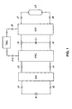
- Figure 1 is a block diagram of a circuit arrangement according to the invention shown.
- a mains voltage source M feeds through the connection points J1 and J2 enters a mains voltage in a block GR.
- the block GR contains a rectifier and may contain means for filtering radio interference.
- the block GR provides a rectified mains voltage at the connection points J3 and J4 to disposal. It feeds the PFC block.
- the block PFC contains one Power factor correction device. It can be any, from act topology known in literature. For example, a step-up, Buck converter or SEPIC topology can be used. It is important for the invention that the power factor correction device is not automatic when a Mains voltage at J4 and J4 starts to oscillate. According to the block PFC a connection point J10. The power factor correction device is oscillated via J10 started. After starting, the power factor correction device can oscillate automatically. A start signal does not have to be permanent on J10 issue.
- the block PFC provides a storage capacitor via the connection points J5 and J6 C1 an intermediate circuit voltage is available.
- the DC link voltage provides energy for a block INV.
- the discharge lamp LP represents high and low pressure discharge lamps. Several lamps can also be connected in series or in parallel to J7 and J8 are connected. For low pressure discharge lamps with heated electrode filaments can also provide further connections for the lamps his.
- connection point J9 which shows when the inverter is oscillating in the INV block.
- a logic signal of an oscillator module can be output via J9. in the In the simplest case, the oscillation of the inverter itself is applied to J9.
- the signal at J9 is a first connection of a starting device TRG fed.
- a second connection of the starting device TRG is with the Connection point J10 connected via an oscillation of the power factor correction device can be started.
- arrows indicate the direction of action the starting device from J9 to J10.
- the starting device consists only of an electrical connection line. This is only possible if block INV sends a signal to J9 provides, which is directly suitable, an oscillation of the power factor correction device to start. In most applications, however, the starting device must adapt the signal to J9 so that a start according to the invention via J10
- the power factor correction device oscillates. That can mean that the signal at J9 needs to be amplified, weakened or filtered.
- the signal at J10 must be so strong that the power factor correction device starts to oscillate can be done. It must not be so strong that it started Oscillation affected. And there must be no possibility of a start that contradicts the inventive idea.
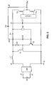
- Figure 2 is a circuit diagram of an embodiment of an inventive Circuit arrangement shown.
- the connection points J4 and J6 combined to a ground potential G.
- the block delivers at J3 GR a rectified mains voltage with respect to the ground potential G.
- T1 forms the step-up switch
- L1 the Booster choke
- D1 the step-up diode
- a first connection from L1 is connected to J3.
- a second port of L1 is connected to junction J10, which is a start input of the step-up converter forms.
- T1 is designed as a MOSFET, whose channel is between J10 and the ground potential G is switched.
- the gate of T1 is connected to J10 via resistor R 1.
- the gate is also connected to the collector of transistor T2, which is called Bipolar transistor is executed.
- the emitter of T2 has the ground potential G connected.
- the base of T2 is connected to J10 via capacitor C3.
- the base of T2 is also connected to a connection point J5 via resistor R2.
- a storage capacitor C1 is located between J5 and ground potential G. connected. An intermediate circuit voltage is therefore present at J5 in relation to the ground potential G. on.
- the diode D1 is with its anode with J10 and with its cathode with J5 connected.
- the series circuit connection of two half-bridge transistors is connected to the intermediate circuit voltage T3 and T4 switched.
- the gate connections of T3 and T4 are made by one Block CONT controlled.
- the block CONT can contain a high-frequency oscillator, the T3 and T4 alternately turn on and off. It is also possible that the block CONT receives a half-bridge feedback signal and depends on it transistors T3 and T4 alternately turn on and off. In this case with the block CONT, T3 and T4 a self-oscillating half-bridge inverter built up.
- connection point Out is connected to the connection point J9. Is on J9 thus the oscillation of the half-bridge inverter in the form of a high-frequency AC voltage on. J9 is connected to J10 via a trigger capacitor C2.
- the comparison with FIG. 1 shows that the starting device in the application example in FIG Figure 2 is realized by the trigger capacitor C2.
- T2 When commissioning the circuit arrangement, T2 is first via C3, after the structure of the DC link voltage is also controlled via R2. This will over T2 the gate of T1 connected to the ground potential G. An oscillation of the self-oscillating step-up converter is therefore not started.
- the intermediate circuit voltage When charging of the storage capacitor is largely completed, the intermediate circuit voltage is reached a value that enables the half-bridge inverter to oscillate. This oscillation reduces the base-emitter voltage via the capacitors C2 and C3 from T2. T2 switches off and T1 can be switched on via R1.
- the oscillation of the power factor correction device sets only after the charging process of the storage capacitor during commissioning the circuit arrangement is largely completed. Problems described above with high charging currents are avoided.
- Figure 3 is the circuit diagram of another embodiment of an inventive Circuit arrangement shown. In comparison to Figure 2 is the circuit diagram in Figure 3 by an overvoltage shutdown OV and an error shutdown SD extended.
- the overvoltage switch-off OV detects the intermediate circuit voltage.
- Terminal 1 is connected to the gate of T1. exceeds the intermediate circuit voltage a predetermined overvoltage threshold, the gate of T1 is connected to ground potential G via connections 1 and 2. This stops the oscillation of the power factor correction device.
- the half-bridge transistor T4 is via a Measuring resistor R3 connected to the ground potential G.
- the voltage drop on R3 is a measure of the current in the half-bridge.
- This also happens in the fault shutdown SD via connection 4. It is also possible from the voltage across the discharge lamp To derive errors. To do this, this voltage must be used for fault shutdown SD are fed.
- the SD fault lock detects a fault, it interrupts the connection 6 the oscillation of the half-bridge inverter. Interrupts according to the invention the fault shutdown SD the oscillation of the half-bridge inverter permanent.
- the oscillation of the half-bridge inverter can only be influenced from outside release again. This can be caused by an interruption, for example the mains voltage.
- the SD fault shutdown is via the connections 5 and 7 connected to the DC link voltage. Ports 5 and 7 can also be used to supply the SD with fault voltage.
- the DC link voltage drops due to an interruption in the mains voltage and resets the SD fault lock. When the DC link voltage rises again the oscillation of the half-bridge inverter can start again.
- Means can also be provided for renewed oscillation of the half-bridge inverter enable after changing the lamp.
- the permanent interruption of the oscillation of the half-bridge inverter leads in the illustrated embodiment to a steady increase in the intermediate circuit voltage. Finally, the value of the DC link voltage exceeds the overvoltage threshold. The surge cut-off then stops the oscillation the power factor correction device. It is also after the switch-off time no longer started if the half-bridge inverter does not restart oscillates. The circuit arrangement is thus in a switch-off mode.
Landscapes
- Circuit Arrangements For Discharge Lamps (AREA)
- Inverter Devices (AREA)
- Dc-Dc Converters (AREA)
- Rectifiers (AREA)
Applications Claiming Priority (2)
| Application Number | Priority Date | Filing Date | Title |
|---|---|---|---|
| DE10241327 | 2002-09-04 | ||
| DE10241327A DE10241327A1 (de) | 2002-09-04 | 2002-09-04 | Schaltungsanordnung zum Betrieb von Entladungslampen |
Publications (3)
| Publication Number | Publication Date |
|---|---|
| EP1397029A2 true EP1397029A2 (fr) | 2004-03-10 |
| EP1397029A3 EP1397029A3 (fr) | 2005-07-06 |
| EP1397029B1 EP1397029B1 (fr) | 2006-10-11 |
Family
ID=31502452
Family Applications (1)
| Application Number | Title | Priority Date | Filing Date |
|---|---|---|---|
| EP03017860A Expired - Lifetime EP1397029B1 (fr) | 2002-09-04 | 2003-08-05 | Circuit pour opérer une lampe de décharge |
Country Status (8)
| Country | Link |
|---|---|
| US (1) | US6833678B2 (fr) |
| EP (1) | EP1397029B1 (fr) |
| KR (1) | KR100968082B1 (fr) |
| CN (1) | CN100544538C (fr) |
| AT (1) | ATE342648T1 (fr) |
| CA (1) | CA2438719A1 (fr) |
| DE (2) | DE10241327A1 (fr) |
| TW (1) | TWI283423B (fr) |
Cited By (3)
| Publication number | Priority date | Publication date | Assignee | Title |
|---|---|---|---|---|
| EP1530407A3 (fr) * | 2003-11-05 | 2007-01-17 | Patent-Treuhand-Gesellschaft für elektrische Glühlampen mbH | Ballast électronique dans lequel le convertisseur reste actif en cas de défaillance de la lampe |
| WO2011018324A1 (fr) * | 2009-08-10 | 2011-02-17 | Osram Gesellschaft mit beschränkter Haftung | Procédé de régulation d'un transformateur de tension aux fins de protection contre les surtensions, transformateur de tension, et équipement comportant un transformateur de tension |
| DE102011100005A1 (de) * | 2011-04-29 | 2012-10-31 | Tridonic Gmbh & Co. Kg | Verfahren und Schaltung zur Leistungsfaktorkorrektur |
Families Citing this family (10)
| Publication number | Priority date | Publication date | Assignee | Title |
|---|---|---|---|---|
| US6934168B2 (en) * | 2003-02-27 | 2005-08-23 | International Rectifier Corporation | Single stage PFC and power converter unit |
| US7075251B2 (en) * | 2003-12-05 | 2006-07-11 | General Electric Company | Universal platform for phase dimming discharge lighting ballast and lamp |
| DE102005028419A1 (de) * | 2005-06-20 | 2006-12-28 | Patent-Treuhand-Gesellschaft für elektrische Glühlampen mbH | Abschaltschaltung |
| KR100771622B1 (ko) * | 2006-02-13 | 2007-10-30 | 엘지전자 주식회사 | 피에프씨 과전압 차단장치 |
| DE102006017341A1 (de) * | 2006-04-11 | 2007-10-18 | Patent-Treuhand-Gesellschaft für elektrische Glühlampen mbH | Reduzierte Verlustleistung in Elektronischen Vorschaltgeräten (EVGs) |
| KR100855030B1 (ko) * | 2007-05-02 | 2008-08-29 | 금호전기주식회사 | 다중 보호회로를 구비한 전자식 방전램프 구동장치 |
| DE102009023884A1 (de) * | 2009-06-04 | 2011-01-27 | Osram Gesellschaft mit beschränkter Haftung | Elektronisches Vorschaltgerät und Verfahren zum Betreiben mindestens einer Entladungslampe |
| FR2980314B1 (fr) | 2011-09-16 | 2013-10-18 | R2R Dev | Appareil d'eclairage public |
| CN104333213B (zh) * | 2014-11-25 | 2018-04-10 | 阳光电源股份有限公司 | 一种pv阵列输出过压时的保护方法、设备及系统 |
| US9531255B2 (en) | 2015-01-12 | 2016-12-27 | Technical Consumer Products, Inc. | Low-cost driver circuit with improved power factor |
Family Cites Families (13)
| Publication number | Priority date | Publication date | Assignee | Title |
|---|---|---|---|---|
| US5510974A (en) * | 1993-12-28 | 1996-04-23 | Philips Electronics North America Corporation | High frequency push-pull converter with input power factor correction |
| ATE179843T1 (de) * | 1994-02-10 | 1999-05-15 | Koninkl Philips Electronics Nv | Hochfrequenter wechselstromwandler mit leistungsfaktorkorrektur |
| US5471117A (en) * | 1994-05-11 | 1995-11-28 | Mti International, Inc. | Low power unity power factor ballast |
| US5583398A (en) * | 1994-09-15 | 1996-12-10 | Magnetek, Inc. | Powerfactor correcting flyback arrangement having a resonant capacitor element connected across the switching element |
| US5569984A (en) * | 1994-12-28 | 1996-10-29 | Philips Electronics North America Corporation | Method and controller for detecting arc instabilities in gas discharge lamps |
| US5568041A (en) * | 1995-02-09 | 1996-10-22 | Magnetek, Inc. | Low-cost power factor correction circuit and method for electronic ballasts |
| US5498936A (en) * | 1995-03-31 | 1996-03-12 | Smith; Jerry J. | Power system with simplified, low cost self-starting self oscillator, power factor correction, power regulation and output open circuit voltage regulation, overload and short circuit protection |
| US6486615B2 (en) * | 1998-10-13 | 2002-11-26 | City University Of Hong Kong | Dimming control of electronic ballasts |
| US6172466B1 (en) * | 1999-02-12 | 2001-01-09 | The Hong Kong University Of Science And Technology | Phase-controlled dimmable ballast |
| KR100335990B1 (ko) * | 1999-08-27 | 2002-05-10 | 윤덕용 | 형광등용 전자식 안정기의 역률 개선회로 |
| US6359394B1 (en) * | 1999-12-22 | 2002-03-19 | Phillips Electronics North America Corporation | Scheme for sampling lamp conditions during ignition and steady state modes of lamp operation |
| US6501235B2 (en) * | 2001-02-27 | 2002-12-31 | Stmicroelectronics Inc. | Microcontrolled ballast compatible with different types of gas discharge lamps and associated methods |
| DE10200049A1 (de) * | 2002-01-02 | 2003-07-17 | Patent Treuhand Ges Fuer Elektrische Gluehlampen Mbh | Betriebsgerät für Gasentladungslampen |
-
2002
- 2002-09-04 DE DE10241327A patent/DE10241327A1/de not_active Withdrawn
-
2003
- 2003-08-04 TW TW092121278A patent/TWI283423B/zh not_active IP Right Cessation
- 2003-08-05 EP EP03017860A patent/EP1397029B1/fr not_active Expired - Lifetime
- 2003-08-05 DE DE50305331T patent/DE50305331D1/de not_active Expired - Lifetime
- 2003-08-05 AT AT03017860T patent/ATE342648T1/de not_active IP Right Cessation
- 2003-08-25 KR KR1020030058683A patent/KR100968082B1/ko not_active Expired - Fee Related
- 2003-08-25 US US10/646,870 patent/US6833678B2/en not_active Expired - Fee Related
- 2003-08-25 CA CA002438719A patent/CA2438719A1/fr not_active Abandoned
- 2003-09-04 CN CNB031554571A patent/CN100544538C/zh not_active Expired - Fee Related
Cited By (5)
| Publication number | Priority date | Publication date | Assignee | Title |
|---|---|---|---|---|
| EP1530407A3 (fr) * | 2003-11-05 | 2007-01-17 | Patent-Treuhand-Gesellschaft für elektrische Glühlampen mbH | Ballast électronique dans lequel le convertisseur reste actif en cas de défaillance de la lampe |
| DE10351621B4 (de) * | 2003-11-05 | 2013-05-16 | Osram Gmbh | Elektronisches Vorschaltgerät sowie Verfahren mit bei Ausfall der Licht emittierenden Einrichtung weiterzubetreibenden Wandler |
| WO2011018324A1 (fr) * | 2009-08-10 | 2011-02-17 | Osram Gesellschaft mit beschränkter Haftung | Procédé de régulation d'un transformateur de tension aux fins de protection contre les surtensions, transformateur de tension, et équipement comportant un transformateur de tension |
| US9125281B2 (en) | 2009-08-10 | 2015-09-01 | Osram Gesellschaft Mit Beschrankter Haftung | Method for controlling a voltage transformer for overvoltage protection, voltage transformer and operating device having a voltage transformer |
| DE102011100005A1 (de) * | 2011-04-29 | 2012-10-31 | Tridonic Gmbh & Co. Kg | Verfahren und Schaltung zur Leistungsfaktorkorrektur |
Also Published As
| Publication number | Publication date |
|---|---|
| KR20040021531A (ko) | 2004-03-10 |
| DE10241327A1 (de) | 2004-03-18 |
| CA2438719A1 (fr) | 2004-03-04 |
| DE50305331D1 (de) | 2006-11-23 |
| US20040080283A1 (en) | 2004-04-29 |
| TW200405381A (en) | 2004-04-01 |
| KR100968082B1 (ko) | 2010-07-08 |
| CN100544538C (zh) | 2009-09-23 |
| CN1496211A (zh) | 2004-05-12 |
| ATE342648T1 (de) | 2006-11-15 |
| TWI283423B (en) | 2007-07-01 |
| US6833678B2 (en) | 2004-12-21 |
| EP1397029A3 (fr) | 2005-07-06 |
| EP1397029B1 (fr) | 2006-10-11 |
Similar Documents
| Publication | Publication Date | Title |
|---|---|---|
| DE69117008T2 (de) | Wechselrichteranordnung | |
| EP0359860A1 (fr) | Dispositif et procédé de mise en oeuvre d'au moins une lampe à décharge | |
| EP1397029B1 (fr) | Circuit pour opérer une lampe de décharge | |
| EP0496246A1 (fr) | Circuit d'alimentation d'une lampe à décharge | |
| DE3829388A1 (de) | Schaltungsanordnung zum betrieb einer last | |
| DE112012001950T5 (de) | Selbstangeregter Gegentaktwandler | |
| DE102005007346A1 (de) | Schaltungsanordnung und Verfahren zum Betreiben von Gasentladungslampen | |
| EP0699016A2 (fr) | Circuit pour alimenter des lampes à décharge basse pression | |
| EP0917412A2 (fr) | Circuit auto-oscillant avec circuit de démarrage simplifié | |
| EP1202612A2 (fr) | Dispositif d'éclairage à préchauffage amélioré pour lampes à décharge | |
| CH660826A5 (de) | Leuchtvorrichtung mit einer gasentladungslampe und ein verfahren zu deren betrieb. | |
| DE19830368A1 (de) | Elektronisches Vorschaltgerät mit Einschaltstrombegrenzung | |
| EP2168229A1 (fr) | Ensemble circuit pourvu d'un transformateur de tension et procédé correspondant | |
| EP1326484B1 (fr) | Appareil pour alimenter des lampes à décharge | |
| EP1729546A1 (fr) | Ballast électronique pour au moins une lampe | |
| EP0389847B1 (fr) | Circuit | |
| EP0276460B1 (fr) | Disposition de circuit pour mettre en oeuvre une lampe à décharge basse pression | |
| EP1028606B1 (fr) | Circuit pour alimenter au moins une lampe à décharge à basse pression | |
| EP0904619B1 (fr) | Circuit pour inverser la polarite d'une tension | |
| EP0871347A1 (fr) | Ballast à réamorçage automatique | |
| DE69714163T2 (de) | Schaltungsanordnung | |
| EP0949851B1 (fr) | Ballast pour lampe à décharge à faible pression | |
| EP1517592B1 (fr) | Circuit pour produire une tension alternative d'une tension continue | |
| DE4335375B4 (de) | Netzgerät zur Speisung einer Gasentladungslampe | |
| DE102004044180A1 (de) | Elektronisches Vorschaltgerät mit Pumpschaltung für Entladungslampe mit vorheizbaren Elektroden |
Legal Events
| Date | Code | Title | Description |
|---|---|---|---|
| PUAI | Public reference made under article 153(3) epc to a published international application that has entered the european phase |
Free format text: ORIGINAL CODE: 0009012 |
|
| REG | Reference to a national code |
Ref country code: SE Ref legal event code: TRGR |
|
| AK | Designated contracting states |
Kind code of ref document: A2 Designated state(s): AT BE BG CH CY CZ DE DK EE ES FI FR GB GR HU IE IT LI LU MC NL PT RO SE SI SK TR |
|
| AX | Request for extension of the european patent |
Extension state: AL LT LV MK |
|
| PUAL | Search report despatched |
Free format text: ORIGINAL CODE: 0009013 |
|
| AK | Designated contracting states |
Kind code of ref document: A3 Designated state(s): AT BE BG CH CY CZ DE DK EE ES FI FR GB GR HU IE IT LI LU MC NL PT RO SE SI SK TR |
|
| AX | Request for extension of the european patent |
Extension state: AL LT LV MK |
|
| RIC1 | Information provided on ipc code assigned before grant |
Ipc: 7H 05B 41/282 A Ipc: 7H 05B 41/285 B |
|
| 17P | Request for examination filed |
Effective date: 20050808 |
|
| AKX | Designation fees paid |
Designated state(s): AT BE BG CH CY CZ DE DK EE ES FI FR GB GR HU IE IT LI LU MC NL PT RO SE SI SK TR |
|
| GRAP | Despatch of communication of intention to grant a patent |
Free format text: ORIGINAL CODE: EPIDOSNIGR1 |
|
| GRAS | Grant fee paid |
Free format text: ORIGINAL CODE: EPIDOSNIGR3 |
|
| GRAA | (expected) grant |
Free format text: ORIGINAL CODE: 0009210 |
|
| AK | Designated contracting states |
Kind code of ref document: B1 Designated state(s): AT BE BG CH CY CZ DE DK EE ES FI FR GB GR HU IE IT LI LU MC NL PT RO SE SI SK TR |
|
| PG25 | Lapsed in a contracting state [announced via postgrant information from national office to epo] |
Ref country code: IT Free format text: LAPSE BECAUSE OF FAILURE TO SUBMIT A TRANSLATION OF THE DESCRIPTION OR TO PAY THE FEE WITHIN THE PRESCRIBED TIME-LIMIT;WARNING: LAPSES OF ITALIAN PATENTS WITH EFFECTIVE DATE BEFORE 2007 MAY HAVE OCCURRED AT ANY TIME BEFORE 2007. THE CORRECT EFFECTIVE DATE MAY BE DIFFERENT FROM THE ONE RECORDED. Effective date: 20061011 Ref country code: CZ Free format text: LAPSE BECAUSE OF FAILURE TO SUBMIT A TRANSLATION OF THE DESCRIPTION OR TO PAY THE FEE WITHIN THE PRESCRIBED TIME-LIMIT Effective date: 20061011 Ref country code: SK Free format text: LAPSE BECAUSE OF FAILURE TO SUBMIT A TRANSLATION OF THE DESCRIPTION OR TO PAY THE FEE WITHIN THE PRESCRIBED TIME-LIMIT Effective date: 20061011 Ref country code: SI Free format text: LAPSE BECAUSE OF FAILURE TO SUBMIT A TRANSLATION OF THE DESCRIPTION OR TO PAY THE FEE WITHIN THE PRESCRIBED TIME-LIMIT Effective date: 20061011 Ref country code: IE Free format text: LAPSE BECAUSE OF FAILURE TO SUBMIT A TRANSLATION OF THE DESCRIPTION OR TO PAY THE FEE WITHIN THE PRESCRIBED TIME-LIMIT Effective date: 20061011 Ref country code: RO Free format text: LAPSE BECAUSE OF FAILURE TO SUBMIT A TRANSLATION OF THE DESCRIPTION OR TO PAY THE FEE WITHIN THE PRESCRIBED TIME-LIMIT Effective date: 20061011 |
|
| REG | Reference to a national code |
Ref country code: GB Ref legal event code: FG4D Free format text: NOT ENGLISH |
|
| REG | Reference to a national code |
Ref country code: CH Ref legal event code: EP |
|
| REG | Reference to a national code |
Ref country code: IE Ref legal event code: FG4D Free format text: LANGUAGE OF EP DOCUMENT: GERMAN |
|
| REF | Corresponds to: |
Ref document number: 50305331 Country of ref document: DE Date of ref document: 20061123 Kind code of ref document: P |
|
| PG25 | Lapsed in a contracting state [announced via postgrant information from national office to epo] |
Ref country code: DK Free format text: LAPSE BECAUSE OF FAILURE TO SUBMIT A TRANSLATION OF THE DESCRIPTION OR TO PAY THE FEE WITHIN THE PRESCRIBED TIME-LIMIT Effective date: 20070111 Ref country code: BG Free format text: LAPSE BECAUSE OF FAILURE TO SUBMIT A TRANSLATION OF THE DESCRIPTION OR TO PAY THE FEE WITHIN THE PRESCRIBED TIME-LIMIT Effective date: 20070111 |
|
| PG25 | Lapsed in a contracting state [announced via postgrant information from national office to epo] |
Ref country code: ES Free format text: LAPSE BECAUSE OF FAILURE TO SUBMIT A TRANSLATION OF THE DESCRIPTION OR TO PAY THE FEE WITHIN THE PRESCRIBED TIME-LIMIT Effective date: 20070122 |
|
| GBT | Gb: translation of ep patent filed (gb section 77(6)(a)/1977) |
Effective date: 20070122 |
|
| PG25 | Lapsed in a contracting state [announced via postgrant information from national office to epo] |
Ref country code: PT Free format text: LAPSE BECAUSE OF FAILURE TO SUBMIT A TRANSLATION OF THE DESCRIPTION OR TO PAY THE FEE WITHIN THE PRESCRIBED TIME-LIMIT Effective date: 20070319 |
|
| ET | Fr: translation filed | ||
| REG | Reference to a national code |
Ref country code: IE Ref legal event code: FD4D |
|
| PLBE | No opposition filed within time limit |
Free format text: ORIGINAL CODE: 0009261 |
|
| STAA | Information on the status of an ep patent application or granted ep patent |
Free format text: STATUS: NO OPPOSITION FILED WITHIN TIME LIMIT |
|
| 26N | No opposition filed |
Effective date: 20070712 |
|
| BERE | Be: lapsed |
Owner name: PATENT-TREUHAND-GESELLSCHAFT FUR ELEKTRISCHE GLUH Effective date: 20070831 |
|
| REG | Reference to a national code |
Ref country code: CH Ref legal event code: PL |
|
| PG25 | Lapsed in a contracting state [announced via postgrant information from national office to epo] |
Ref country code: LI Free format text: LAPSE BECAUSE OF NON-PAYMENT OF DUE FEES Effective date: 20070831 Ref country code: MC Free format text: LAPSE BECAUSE OF NON-PAYMENT OF DUE FEES Effective date: 20070831 Ref country code: CH Free format text: LAPSE BECAUSE OF NON-PAYMENT OF DUE FEES Effective date: 20070831 Ref country code: NL Free format text: LAPSE BECAUSE OF NON-PAYMENT OF DUE FEES Effective date: 20080301 Ref country code: GR Free format text: LAPSE BECAUSE OF FAILURE TO SUBMIT A TRANSLATION OF THE DESCRIPTION OR TO PAY THE FEE WITHIN THE PRESCRIBED TIME-LIMIT Effective date: 20070112 |
|
| NLV4 | Nl: lapsed or anulled due to non-payment of the annual fee |
Effective date: 20080301 |
|
| PG25 | Lapsed in a contracting state [announced via postgrant information from national office to epo] |
Ref country code: BE Free format text: LAPSE BECAUSE OF NON-PAYMENT OF DUE FEES Effective date: 20070831 |
|
| PG25 | Lapsed in a contracting state [announced via postgrant information from national office to epo] |
Ref country code: EE Free format text: LAPSE BECAUSE OF FAILURE TO SUBMIT A TRANSLATION OF THE DESCRIPTION OR TO PAY THE FEE WITHIN THE PRESCRIBED TIME-LIMIT Effective date: 20061011 |
|
| PG25 | Lapsed in a contracting state [announced via postgrant information from national office to epo] |
Ref country code: AT Free format text: LAPSE BECAUSE OF NON-PAYMENT OF DUE FEES Effective date: 20070805 |
|
| PG25 | Lapsed in a contracting state [announced via postgrant information from national office to epo] |
Ref country code: CY Free format text: LAPSE BECAUSE OF FAILURE TO SUBMIT A TRANSLATION OF THE DESCRIPTION OR TO PAY THE FEE WITHIN THE PRESCRIBED TIME-LIMIT Effective date: 20061011 Ref country code: LU Free format text: LAPSE BECAUSE OF NON-PAYMENT OF DUE FEES Effective date: 20070805 |
|
| PG25 | Lapsed in a contracting state [announced via postgrant information from national office to epo] |
Ref country code: HU Free format text: LAPSE BECAUSE OF FAILURE TO SUBMIT A TRANSLATION OF THE DESCRIPTION OR TO PAY THE FEE WITHIN THE PRESCRIBED TIME-LIMIT Effective date: 20070412 Ref country code: TR Free format text: LAPSE BECAUSE OF FAILURE TO SUBMIT A TRANSLATION OF THE DESCRIPTION OR TO PAY THE FEE WITHIN THE PRESCRIBED TIME-LIMIT Effective date: 20061011 |
|
| PGFP | Annual fee paid to national office [announced via postgrant information from national office to epo] |
Ref country code: SE Payment date: 20110809 Year of fee payment: 9 |
|
| REG | Reference to a national code |
Ref country code: DE Ref legal event code: R081 Ref document number: 50305331 Country of ref document: DE Owner name: OSRAM GMBH, DE Free format text: FORMER OWNER: OSRAM GESELLSCHAFT MIT BESCHRAENKTER HAFTUNG, 81543 MUENCHEN, DE Effective date: 20111128 |
|
| REG | Reference to a national code |
Ref country code: DE Ref legal event code: R081 Ref document number: 50305331 Country of ref document: DE Owner name: OSRAM GMBH, DE Free format text: FORMER OWNER: OSRAM AG, 81543 MUENCHEN, DE Effective date: 20130205 |
|
| REG | Reference to a national code |
Ref country code: SE Ref legal event code: EUG |
|
| PG25 | Lapsed in a contracting state [announced via postgrant information from national office to epo] |
Ref country code: SE Free format text: LAPSE BECAUSE OF NON-PAYMENT OF DUE FEES Effective date: 20120806 |
|
| REG | Reference to a national code |
Ref country code: DE Ref legal event code: R081 Ref document number: 50305331 Country of ref document: DE Owner name: OSRAM GMBH, DE Free format text: FORMER OWNER: OSRAM GMBH, 81543 MUENCHEN, DE Effective date: 20130822 |
|
| PGFP | Annual fee paid to national office [announced via postgrant information from national office to epo] |
Ref country code: FI Payment date: 20140813 Year of fee payment: 12 Ref country code: DE Payment date: 20140821 Year of fee payment: 12 |
|
| PGFP | Annual fee paid to national office [announced via postgrant information from national office to epo] |
Ref country code: FR Payment date: 20140821 Year of fee payment: 12 Ref country code: GB Payment date: 20140820 Year of fee payment: 12 |
|
| REG | Reference to a national code |
Ref country code: DE Ref legal event code: R119 Ref document number: 50305331 Country of ref document: DE |
|
| GBPC | Gb: european patent ceased through non-payment of renewal fee |
Effective date: 20150805 |
|
| PG25 | Lapsed in a contracting state [announced via postgrant information from national office to epo] |
Ref country code: FI Free format text: LAPSE BECAUSE OF NON-PAYMENT OF DUE FEES Effective date: 20150805 |
|
| REG | Reference to a national code |
Ref country code: FR Ref legal event code: ST Effective date: 20160429 |
|
| PG25 | Lapsed in a contracting state [announced via postgrant information from national office to epo] |
Ref country code: GB Free format text: LAPSE BECAUSE OF NON-PAYMENT OF DUE FEES Effective date: 20150805 Ref country code: DE Free format text: LAPSE BECAUSE OF NON-PAYMENT OF DUE FEES Effective date: 20160301 |
|
| PG25 | Lapsed in a contracting state [announced via postgrant information from national office to epo] |
Ref country code: FR Free format text: LAPSE BECAUSE OF NON-PAYMENT OF DUE FEES Effective date: 20150831 |