EP1406300A1 - Anschlusskamm und verfahren zu seiner herstellung - Google Patents
Anschlusskamm und verfahren zu seiner herstellung Download PDFInfo
- Publication number
- EP1406300A1 EP1406300A1 EP02743870A EP02743870A EP1406300A1 EP 1406300 A1 EP1406300 A1 EP 1406300A1 EP 02743870 A EP02743870 A EP 02743870A EP 02743870 A EP02743870 A EP 02743870A EP 1406300 A1 EP1406300 A1 EP 1406300A1
- Authority
- EP
- European Patent Office
- Prior art keywords
- portions
- leadframe
- metal plate
- plating
- palladium
- Prior art date
- Legal status (The legal status is an assumption and is not a legal conclusion. Google has not performed a legal analysis and makes no representation as to the accuracy of the status listed.)
- Granted
Links
Images



Classifications
-
- H—ELECTRICITY
- H10—SEMICONDUCTOR DEVICES; ELECTRIC SOLID-STATE DEVICES NOT OTHERWISE PROVIDED FOR
- H10W—GENERIC PACKAGES, INTERCONNECTIONS, CONNECTORS OR OTHER CONSTRUCTIONAL DETAILS OF DEVICES COVERED BY CLASS H10
- H10W70/00—Package substrates; Interposers; Redistribution layers [RDL]
- H10W70/01—Manufacture or treatment
- H10W70/04—Manufacture or treatment of leadframes
- H10W70/042—Etching
-
- H—ELECTRICITY
- H10—SEMICONDUCTOR DEVICES; ELECTRIC SOLID-STATE DEVICES NOT OTHERWISE PROVIDED FOR
- H10W—GENERIC PACKAGES, INTERCONNECTIONS, CONNECTORS OR OTHER CONSTRUCTIONAL DETAILS OF DEVICES COVERED BY CLASS H10
- H10W70/00—Package substrates; Interposers; Redistribution layers [RDL]
- H10W70/40—Leadframes
-
- H—ELECTRICITY
- H10—SEMICONDUCTOR DEVICES; ELECTRIC SOLID-STATE DEVICES NOT OTHERWISE PROVIDED FOR
- H10W—GENERIC PACKAGES, INTERCONNECTIONS, CONNECTORS OR OTHER CONSTRUCTIONAL DETAILS OF DEVICES COVERED BY CLASS H10
- H10W70/00—Package substrates; Interposers; Redistribution layers [RDL]
- H10W70/01—Manufacture or treatment
- H10W70/04—Manufacture or treatment of leadframes
-
- H—ELECTRICITY
- H10—SEMICONDUCTOR DEVICES; ELECTRIC SOLID-STATE DEVICES NOT OTHERWISE PROVIDED FOR
- H10W—GENERIC PACKAGES, INTERCONNECTIONS, CONNECTORS OR OTHER CONSTRUCTIONAL DETAILS OF DEVICES COVERED BY CLASS H10
- H10W70/00—Package substrates; Interposers; Redistribution layers [RDL]
- H10W70/40—Leadframes
- H10W70/456—Materials
- H10W70/457—Materials of metallic layers on leadframes
-
- H—ELECTRICITY
- H05—ELECTRIC TECHNIQUES NOT OTHERWISE PROVIDED FOR
- H05K—PRINTED CIRCUITS; CASINGS OR CONSTRUCTIONAL DETAILS OF ELECTRIC APPARATUS; MANUFACTURE OF ASSEMBLAGES OF ELECTRICAL COMPONENTS
- H05K3/00—Apparatus or processes for manufacturing printed circuits
- H05K3/30—Assembling printed circuits with electric components, e.g. with resistors
- H05K3/32—Assembling printed circuits with electric components, e.g. with resistors electrically connecting electric components or wires to printed circuits
- H05K3/34—Assembling printed circuits with electric components, e.g. with resistors electrically connecting electric components or wires to printed circuits by soldering
- H05K3/341—Surface mounted components
- H05K3/3421—Leaded components
- H05K3/3426—Leaded components characterised by the leads
-
- H—ELECTRICITY
- H10—SEMICONDUCTOR DEVICES; ELECTRIC SOLID-STATE DEVICES NOT OTHERWISE PROVIDED FOR
- H10W—GENERIC PACKAGES, INTERCONNECTIONS, CONNECTORS OR OTHER CONSTRUCTIONAL DETAILS OF DEVICES COVERED BY CLASS H10
- H10W72/00—Interconnections or connectors in packages
- H10W72/071—Connecting or disconnecting
- H10W72/075—Connecting or disconnecting of bond wires
-
- H—ELECTRICITY
- H10—SEMICONDUCTOR DEVICES; ELECTRIC SOLID-STATE DEVICES NOT OTHERWISE PROVIDED FOR
- H10W—GENERIC PACKAGES, INTERCONNECTIONS, CONNECTORS OR OTHER CONSTRUCTIONAL DETAILS OF DEVICES COVERED BY CLASS H10
- H10W72/00—Interconnections or connectors in packages
- H10W72/50—Bond wires
- H10W72/551—Materials of bond wires
- H10W72/552—Materials of bond wires comprising metals or metalloids, e.g. silver
- H10W72/5522—Materials of bond wires comprising metals or metalloids, e.g. silver comprising gold [Au]
-
- H—ELECTRICITY
- H10—SEMICONDUCTOR DEVICES; ELECTRIC SOLID-STATE DEVICES NOT OTHERWISE PROVIDED FOR
- H10W—GENERIC PACKAGES, INTERCONNECTIONS, CONNECTORS OR OTHER CONSTRUCTIONAL DETAILS OF DEVICES COVERED BY CLASS H10
- H10W72/00—Interconnections or connectors in packages
- H10W72/50—Bond wires
- H10W72/59—Bond pads specially adapted therefor
-
- H—ELECTRICITY
- H10—SEMICONDUCTOR DEVICES; ELECTRIC SOLID-STATE DEVICES NOT OTHERWISE PROVIDED FOR
- H10W—GENERIC PACKAGES, INTERCONNECTIONS, CONNECTORS OR OTHER CONSTRUCTIONAL DETAILS OF DEVICES COVERED BY CLASS H10
- H10W72/00—Interconnections or connectors in packages
- H10W72/90—Bond pads, in general
- H10W72/951—Materials of bond pads
- H10W72/952—Materials of bond pads comprising metals or metalloids, e.g. PbSn, Ag or Cu
-
- H—ELECTRICITY
- H10—SEMICONDUCTOR DEVICES; ELECTRIC SOLID-STATE DEVICES NOT OTHERWISE PROVIDED FOR
- H10W—GENERIC PACKAGES, INTERCONNECTIONS, CONNECTORS OR OTHER CONSTRUCTIONAL DETAILS OF DEVICES COVERED BY CLASS H10
- H10W90/00—Package configurations
- H10W90/701—Package configurations characterised by the relative positions of pads or connectors relative to package parts
- H10W90/751—Package configurations characterised by the relative positions of pads or connectors relative to package parts of bond wires
- H10W90/756—Package configurations characterised by the relative positions of pads or connectors relative to package parts of bond wires between a chip and a stacked lead frame, conducting package substrate or heat sink
Definitions
- the present invention relates to a leadframe to be used for semiconductor devices and manufacturing method of the same.
- a leadframe is manufactured in such way that a pattern of the leadframe is formed from a metal plate by etching or press processing, then, after palladium plating is carried out to the whole surface of it, semiconductor elements are mounted on the predetermined position, and then, after sealing with resin, cutting is carried out by using a die etc. Finally, separate chips are produced. Such products are in practical use as electronic parts as IC chips.
- the main object of the present invention is to provide a cheaper leadframe by minimizing the amount of palladium used.
- Another object of the present invention is to provide a manufacturing method of leadframe by which the fault of the leadframe is eliminated.
- the leadframe according to the present invention is characterized in that, in a leadframe which is formed from a metal plate, palladium plating is partially carried out only to necessary and minimum portions on which semiconductor elements are to be mounted, portions to bond gold wires and portions to be soldered of a surface to be placed on a printed circuit board.
- the leadframe according to the present invention is characterized in that, in a leadframe which is formed from a metal plate, palladium plating is carried out only to a surface on which semiconductor elements are to be mounted and a surface to be placed on a printed circuit board, and that the palladium plating is not carried out to lead portions formed, pad portions, other portions except for the surfaces to be plated and its side surface.
- the leadframe according to the present invention is characterized in that, in a leadframe which is formed from a metal plate, palladium plating is carried out only to necessary and minimum portions of a surface on which semiconductor elements are to be mounted and a surface to be placed on a printed circuit board, the palladium plating is not carried out to lead portions formed, pad portions, other portions except for the portions of the surfaces to be plated and its side surface.
- a leadframe material is provided by forming a metal plate, and then, palladium plating is carried out only to portions which are necessary and minimum for mounting of semiconductor elements of the leadframe material, and then, the plating is carried out to portions to bond gold wires and necessary and minimum portions to be soldered of a surface to be placed on a printed circuit board, of the leadframe material.
- a leadframe material is provided by forming a metal plate, and then, palladium plating is carried out only to a surface of the leadframe material on which semiconductor elements are to be mounted, and then, the plating is carried out only to a surface of the leadframe material to be placed on a printed circuit board, while the plating is not carried out to lead portions, pad portions, other portions except for the surfaces to be plated and the side surface of the leadframe material.
- a metal plate is prepared to form a leadframe, and then, a resist layer is formed on the both sides of the metal plate.
- a mask e.g. a mask, which is closely attached to the surface of the resist layer, for exposing light, developing and plating
- the surface of the exposed metal plate is plated, wherein the plated layers containing at least palladium plated layer are formed and then the mask is stripped, and a resist layer is again formed on the whole both sides of the plate.
- an etching mask is obtained. And then, the shape of lead portions, pad portions and other portions are formed by etching.
- a metal plate is provided to form a leadframe by forming the metal plate and then a resist layer is formed on the both front and back surfaces of the metal plate. And after having made a mask (e.g. a mask, which is closely attached to the surfaces of the resist layer for exposing light, developing and plating) with a desired pattern of the leadframe on the surface of the resist layer, the surface of the exposed metal plate is plated, wherein plated layers containing at least palladium plated layer is formed.
- a mask e.g. a mask, which is closely attached to the surfaces of the resist layer for exposing light, developing and plating
- the resist layer is removed, etching of the metal plate is carried out by using the plated layer as an etching resist, wherein the etching is stopped before the portions of the metal plate which is necessary to be etched are penetrated by the etching. And then, the back surface of the metal plate is masked with a tape, and the portion of the metal plate, which is necessary to be etched, is penetrated by carrying out etching again.
- the relation of positions of a number of lead portions etc. can be kept individually and independently by the tape.
- a metal plate is provided to form a leadframe and then a resist layer is formed on the both sides of the metal plate.
- a mask e. g. a mask for carrying out etching which is closely attached to the surface of the resist layer for exposing light, and then developing
- the exposed metal plate portion is removed by the etching and the pattern of leadframe is formed.
- the both front and back surfaces of the leadframe are plated so as to form a plated layer containing at least palladium layer.
- a metal plate is provided to form a leadframe and a resist layer is formed on the both front and back surfaces of the metal plate.
- a mask e.g. a mask for carrying out plating which is closely attached to the surface of the resist layer and to which light is exposed and then developing is carried out
- the surface of the exposed metal plate is plated, thereby, plated layers containing at least palladium plated layer are formed.
- the resist layer is removed and etching of the metal plate is carried out by using the plated layer as an etching resist.
- the leadframe which is not only cheaper but also does not cause such fault as missing of lead, breakage of resin etc., as seen in the conventional leadframe can be provided since it is good enough to cut only the resin portion at the time when the leadframe is cut into small chips by using the cutting or dicing device etc., after semiconductor elements are mounted on the predetermined position on the leadframe and sealing is made by resin because the metal portions to be cut has already dissolved by the etching.
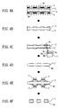
- Fig. 1 is a flowchart illustrating an embodiment of the manufacturing method of leadframe according to the present invention.
- 1 is a plate of copper or similar material for forming a leadframe.
- 2 is a dry film mounted on the front and back surface of the metal plate 1.
- 3 is a glass mask which is put on the dry film 2 placed on the surface of the metal plate 1, and which forms a leadframe pattern 3a by using a light shielding agent.
- 4 is a glass mask which is put on the dry film 2 placed on the back surface of the metal plate 1, and which forms a leadframe pattern 4a on symmetrically opposite side to the leadframe pattern 3a with respect to the metal plate 1 by using the light shielding agent.
- 5 and 6 are glass masks which form predetermined shading patterns
- 7 are a plurality of etching liquid injection nozzles which are disposed oppositely at both sides of the metal plate 1.
- the manufacturing process of the leadframe will be explained in turn.
- the dry film 2 working as photoresist is placed on the whole front and back surfaces of the metal plate 1.
- the glass masks 3 and 4 which have the leadframe patterns 3a and 4a are put on the front and back surfaces at the state of positioning of the pattern. And such both surfaces are exposed by the ultra violet ray through the glass masks 3 and 4.
- the glass masks 3 and 4 are removed and the metal plate 1 with dry film is soaked into the developing solution for development.
- the portions of the dry film 2 exposed by the ultra violet ray i.e., portions which are necessary to be plated with palladium, such as portions to which gold wires are bonded and portions for mounting thereon semiconductor elements are removed as shown in Fig.1 B.
- the dry film 2 is again placed on the whole both front and back surfaces of the metal plate 1 with the plated layer 1a which was obtained in the way as described above. Then, as shown in Fig. 1E, the glass masks 5 and 6 on which the pattern is formed so as to shade only the plated portions are put on the film 2 and the both sides are again exposed by the ultra violet ray. Then, as explained in Fig. 1B, the development is carried out, and the metal plate 1 with the plated layer 1a of the cross-sectional configuration as shown in Fig. 1F is obtained.
- etching is carried out by spraying etching liquid through the injection nozzles 7 on the both surfaces of the metal plate 1 with plated layer 1a.
- etching the metal portions on which plating is not carried out is dissolved and removed.
- stripping the dry film 2 one frame of the leadframe which has the cross-sectional configuration as shown in Fig.1H, that is, on which plating was carried out only to the necessary minimum portion is obtained.
- Each process shown in Figs. 1A to 1H is carried out continuously by conveying a metal plate having the length including a plurality of frames on an appropriate conveyer and each frame of the leadframe is completed after being cut at the final stage of the process.
- palladium plating is carried out only to necessary portions of the front and back surfaces of each leadframe.
- Fig. 2 shows a flowchart illustrating another embodiment of the manufacturing method of leadframe according to the present invention.
- the same reference numerals in Fig.1 are used to the substantially same components and portions, the explanation of the reference numerals are omitted. Since each process shown in Figs. 2A, 2B, 2C and 2D is the same as each process shown in Figs. 1A, 1B, 1C and 1D as it is clearly seen by comparison with Fig. 1,the explanation of such process is omitted, with respect to each process shown after Fig. 2E, the explanation will be made.
- the etching is carried out by spraying the etching liquid through the injection nozzles 7 to the both sides of the metal plate 1 with the plated layer la. Such etching is carried out until the metal of the portion where the plating is not carried out becomes extremely thin in consequence of such metal having been almost dissolved and removed.
- the etching is again carried out by spraying the etching liquid through the injection nozzles 7 from the side to which the tape 8 is not attached as shown in Fig.2G.
- the extremely thin metal portions to which the plating is not carried out unnecessary portions, such as tie bars for connecting lead portions and hanging leads which are to be cut out after the assembling process
- the remained metal portions namely, such necessary portions as portions on which semiconductor elements are to be mounted, pad portions and lead portions where the plating has been carried out are certainly held without collapsing relative positions by the tape 8, as shown in Fig. 2H.
- Fig.3 shows a flowchart illustrating still another embodiment of the manufacturing method of leadframe according to the present invention.
- the same reference numerals in Fig.1 are used to the substantially same components and portions, the explanation of those numeral references is omitted. Since each process shown in Figs. 3A and 3B is the same as the process shown in Figs. 1A and 1B as it is clearly seen in comparison with Fig.1, the explanation of such processes is omitted, with respect to each process shown after Fig.3C, the explanation will be made.
- the etching is carried out by spraying the etching liquid through the injection nozzles 7 on both sides of the metal plate 1 on which the dry film 2 remains corresponding to the leadframe pattern. Such etching is carried out until the metal plate 1 comes to have penetrated holes as a consequence of dissolution and removal of the metal of portions on which the dry film 2 do not exist, as shown in Fig.3D. Thus the dry film 2 is stripped from the both surfaces of the metal plate 1 having the holes. In this way, the leadframe material with cross sectional configuration as shown in Fig.3D is manufactured.
- the nickel (Ni) plating, palladium (Pd) plating, and gold (Au) plating are carried out, respectively, as shown by an enlarged scale in Fig. 3E and then a leadframe is completed. That is to say, as shown in Fig. 3 F, at first, the nickel (Ni) plating is carried out to the whole surface of the front and back surfaces of the leadframe as a ground layer, and then as shown in Fig.3G below, the palladium (Pd) plating is carried out only to the necessary minimum portions for semiconductor mounting portions, portions to bond gold wires and portions to be soldered of the surface to be on a printed circuit board.
- the gold (Au) plating is carried out to the both sides of the front and the back surfaces of the leadframe and then a leadframe is completed.
- the amount of the expensive palladium used can be at a minimum, and the finished product of a leadframe is much cheaper as compared with the conventional leadframe.
- Fig. 4 shows a flowchart of still another embodiment of the manufacturing method of leadframe according to the present invention.
- the same reference numerals used in Fig. 1 are given to the substantially same components and portions and the explanation about them is omitted.
- the explanation of Figs. 4A to 4D is omitted since each process is the same as those of Figs. 1A to 1D as it is evident by comparison with Figs. 1A to 1D.
- the processes shown after Fig. 4E will be explained.
- This embodiment differs from the first embodiment in such point that the product is manufactured by the etching, that is, by spraying the etching liquid through the inj ection nozzles 7 on both sides of the metal plate obtained in Fig.4 D on which the plating was completed without carrying out the second light exposure and the development. According to this embodiment, the product can be provided much cheaper.
- the leadframe which is not only much cheaper but also does not cause fault such as missing of lead and breakage of resin in comparison with the product by the conventional method can be provided.
Landscapes
- Lead Frames For Integrated Circuits (AREA)
- ing And Chemical Polishing (AREA)
- Manufacturing Of Printed Circuit Boards (AREA)
Priority Applications (1)
| Application Number | Priority Date | Filing Date | Title |
|---|---|---|---|
| EP11153697A EP2312630A1 (de) | 2001-07-09 | 2002-07-09 | Leiterrahmen und Verfahren zu seiner Herstellug |
Applications Claiming Priority (3)
| Application Number | Priority Date | Filing Date | Title |
|---|---|---|---|
| JP2001207316A JP4852802B2 (ja) | 2001-06-19 | 2001-07-09 | リードフレーム |
| JP2001207316 | 2001-07-09 | ||
| PCT/JP2002/006933 WO2003007373A1 (en) | 2001-07-09 | 2002-07-09 | Lead frame and its manufacturing method |
Related Child Applications (1)
| Application Number | Title | Priority Date | Filing Date |
|---|---|---|---|
| EP11153697.5 Division-Into | 2011-02-08 |
Publications (3)
| Publication Number | Publication Date |
|---|---|
| EP1406300A1 true EP1406300A1 (de) | 2004-04-07 |
| EP1406300A4 EP1406300A4 (de) | 2007-11-21 |
| EP1406300B1 EP1406300B1 (de) | 2012-02-22 |
Family
ID=19043321
Family Applications (2)
| Application Number | Title | Priority Date | Filing Date |
|---|---|---|---|
| EP02743870A Expired - Lifetime EP1406300B1 (de) | 2001-07-09 | 2002-07-09 | Verfahren zur Herstellung eines Leiterrahmens |
| EP11153697A Ceased EP2312630A1 (de) | 2001-07-09 | 2002-07-09 | Leiterrahmen und Verfahren zu seiner Herstellug |
Family Applications After (1)
| Application Number | Title | Priority Date | Filing Date |
|---|---|---|---|
| EP11153697A Ceased EP2312630A1 (de) | 2001-07-09 | 2002-07-09 | Leiterrahmen und Verfahren zu seiner Herstellug |
Country Status (8)
| Country | Link |
|---|---|
| US (3) | US7235868B2 (de) |
| EP (2) | EP1406300B1 (de) |
| KR (2) | KR100908891B1 (de) |
| CN (1) | CN1317762C (de) |
| AT (1) | ATE546835T1 (de) |
| ES (1) | ES2383874T3 (de) |
| TW (1) | TWI264099B (de) |
| WO (1) | WO2003007373A1 (de) |
Cited By (1)
| Publication number | Priority date | Publication date | Assignee | Title |
|---|---|---|---|---|
| EP2286451A4 (de) * | 2008-06-04 | 2013-10-16 | Nat Semiconductor Corp | Halbleiterpaket auf folienbasis |
Families Citing this family (20)
| Publication number | Priority date | Publication date | Assignee | Title |
|---|---|---|---|---|
| US6943434B2 (en) * | 2002-10-03 | 2005-09-13 | Fairchild Semiconductor Corporation | Method for maintaining solder thickness in flipchip attach packaging processes |
| US8492883B2 (en) * | 2008-03-14 | 2013-07-23 | Advanced Semiconductor Engineering, Inc. | Semiconductor package having a cavity structure |
| US20100044850A1 (en) * | 2008-08-21 | 2010-02-25 | Advanced Semiconductor Engineering, Inc. | Advanced quad flat non-leaded package structure and manufacturing method thereof |
| JP4670931B2 (ja) * | 2008-09-29 | 2011-04-13 | 住友金属鉱山株式会社 | リードフレーム |
| JP5629969B2 (ja) | 2008-09-29 | 2014-11-26 | 凸版印刷株式会社 | リードフレーム型基板の製造方法と半導体装置の製造方法 |
| JP5549066B2 (ja) * | 2008-09-30 | 2014-07-16 | 凸版印刷株式会社 | リードフレーム型基板とその製造方法、及び半導体装置 |
| JP5493323B2 (ja) * | 2008-09-30 | 2014-05-14 | 凸版印刷株式会社 | リードフレーム型基板の製造方法 |
| KR101148100B1 (ko) * | 2008-10-22 | 2012-05-22 | 엘지이노텍 주식회사 | 다열형 리드프레임 및 반도체 패키지의 제조방법 |
| KR101064755B1 (ko) * | 2008-12-24 | 2011-09-15 | 엘지이노텍 주식회사 | 다열 리드형 리드프레임 및 이를 이용한 반도체 패키지의 제조방법 |
| US8124447B2 (en) * | 2009-04-10 | 2012-02-28 | Advanced Semiconductor Engineering, Inc. | Manufacturing method of advanced quad flat non-leaded package |
| US20110163430A1 (en) * | 2010-01-06 | 2011-07-07 | Advanced Semiconductor Engineering, Inc. | Leadframe Structure, Advanced Quad Flat No Lead Package Structure Using the Same, and Manufacturing Methods Thereof |
| CN102324414B (zh) * | 2011-09-13 | 2013-06-26 | 江苏长电科技股份有限公司 | 有基岛预填塑封料先镀后刻引线框结构及其生产方法 |
| CN102403282B (zh) * | 2011-11-22 | 2013-08-28 | 江苏长电科技股份有限公司 | 有基岛四面无引脚封装结构及其制造方法 |
| CN102661829A (zh) * | 2012-04-28 | 2012-09-12 | 无锡永阳电子科技有限公司 | So8塑料封装传感器 |
| CN103413766B (zh) * | 2013-08-06 | 2016-08-10 | 江阴芯智联电子科技有限公司 | 先蚀后封芯片正装三维系统级金属线路板结构及工艺方法 |
| CN103400771B (zh) * | 2013-08-06 | 2016-06-29 | 江阴芯智联电子科技有限公司 | 先蚀后封芯片倒装三维系统级金属线路板结构及工艺方法 |
| CN103456645B (zh) * | 2013-08-06 | 2016-06-01 | 江阴芯智联电子科技有限公司 | 先蚀后封三维系统级芯片正装堆叠封装结构及工艺方法 |
| US10141197B2 (en) * | 2016-03-30 | 2018-11-27 | Stmicroelectronics S.R.L. | Thermosonically bonded connection for flip chip packages |
| JP6777365B2 (ja) * | 2016-12-09 | 2020-10-28 | 大口マテリアル株式会社 | リードフレーム |
| CN113838761A (zh) * | 2021-11-24 | 2021-12-24 | 新恒汇电子股份有限公司 | 物联网工业级卡的制备方法 |
Family Cites Families (32)
| Publication number | Priority date | Publication date | Assignee | Title |
|---|---|---|---|---|
| JPS6050349B2 (ja) * | 1980-07-09 | 1985-11-08 | 住友金属鉱山株式会社 | リ−ドフレ−ムの製造方法 |
| US4770899A (en) | 1987-06-10 | 1988-09-13 | Unisys Corporation | Method of coating copper conductors on polyimide with a corrosion resistant metal, and module produced thereby |
| JP2807505B2 (ja) * | 1989-10-20 | 1998-10-08 | 新光電気工業株式会社 | リードフレームの製造方法 |
| KR920008359Y1 (ko) * | 1989-11-28 | 1992-11-20 | 현대전자산업 주식회사 | 리드프레임 |
| US5235139A (en) | 1990-09-12 | 1993-08-10 | Macdermid, Incorprated | Method for fabricating printed circuits |
| US5234139A (en) * | 1991-08-06 | 1993-08-10 | Korenstein Michael W | Apparatus for the management of paired garments |
| JP3275413B2 (ja) * | 1993-01-21 | 2002-04-15 | 凸版印刷株式会社 | リードフレームおよびその製造方法 |
| JP2004343136A (ja) * | 1995-09-29 | 2004-12-02 | Dainippon Printing Co Ltd | 半導体装置 |
| US5804880A (en) * | 1996-11-04 | 1998-09-08 | National Semiconductor Corporation | Solder isolating lead frame |
| EP1021831A1 (de) * | 1997-01-30 | 2000-07-26 | GCB Technologies, Inc | Verbesserte leiterrahmerstruktur mit vorplatierten fingern und herstellungsverfahren dafür |
| DE19704689A1 (de) * | 1997-02-07 | 1998-08-13 | Emitec Emissionstechnologie | Wabenkörper mit im Inneren freiem Querschnittsbereich, insbesondere für Kleinmotoren |
| US5923090A (en) * | 1997-05-19 | 1999-07-13 | International Business Machines Corporation | Microelectronic package and fabrication thereof |
| CN1068064C (zh) * | 1997-05-27 | 2001-07-04 | 旭龙精密工业股份有限公司 | 引线框架及其制造方法 |
| US6025640A (en) * | 1997-07-16 | 2000-02-15 | Dai Nippon Insatsu Kabushiki Kaisha | Resin-sealed semiconductor device, circuit member for use therein and method of manufacturing resin-sealed semiconductor device |
| EP0921562A3 (de) * | 1997-10-28 | 2002-06-05 | Texas Instruments Incorporated | Verbesserungen an oder in Beziehung zu Leiterrahmen |
| KR100275381B1 (ko) * | 1998-04-18 | 2000-12-15 | 이중구 | 반도체 패키지용 리드프레임 및 리드프레임도금방법 |
| JP4156087B2 (ja) * | 1998-08-07 | 2008-09-24 | 大日本印刷株式会社 | 電着処理装置 |
| US6451627B1 (en) * | 1999-09-07 | 2002-09-17 | Motorola, Inc. | Semiconductor device and process for manufacturing and packaging a semiconductor device |
| US6469386B1 (en) * | 1999-10-01 | 2002-10-22 | Samsung Aerospace Industries, Ltd. | Lead frame and method for plating the same |
| KR100450091B1 (ko) * | 1999-10-01 | 2004-09-30 | 삼성테크윈 주식회사 | 반도체 장치용 다층 도금 리드 프레임 |
| JP2001185670A (ja) * | 1999-12-10 | 2001-07-06 | Texas Instr Inc <Ti> | リードフレームとその製法 |
| KR100421774B1 (ko) | 1999-12-16 | 2004-03-10 | 앰코 테크놀로지 코리아 주식회사 | 반도체패키지 및 그 제조 방법 |
| US6827584B2 (en) * | 1999-12-28 | 2004-12-07 | Formfactor, Inc. | Interconnect for microelectronic structures with enhanced spring characteristics |
| US7026710B2 (en) * | 2000-01-21 | 2006-04-11 | Texas Instruments Incorporated | Molded package for micromechanical devices and method of fabrication |
| US6238952B1 (en) * | 2000-02-29 | 2001-05-29 | Advanced Semiconductor Engineering, Inc. | Low-pin-count chip package and manufacturing method thereof |
| KR100371567B1 (ko) * | 2000-12-08 | 2003-02-07 | 삼성테크윈 주식회사 | Ag 선도금을 이용한 반도체 패키지용 리드프레임 |
| US20020170878A1 (en) * | 2001-03-27 | 2002-11-21 | Bmc Industries, Inc. | Etching resistance of protein-based photoresist layers |
| JP2002299540A (ja) * | 2001-04-04 | 2002-10-11 | Hitachi Ltd | 半導体装置およびその製造方法 |
| JP4173346B2 (ja) * | 2001-12-14 | 2008-10-29 | 株式会社ルネサステクノロジ | 半導体装置 |
| US6713852B2 (en) * | 2002-02-01 | 2004-03-30 | Texas Instruments Incorporated | Semiconductor leadframes plated with thick nickel, minimum palladium, and pure tin |
| JP2003297994A (ja) * | 2002-03-29 | 2003-10-17 | Hitachi Ltd | 半導体装置およびその製造方法 |
| TW558776B (en) * | 2002-08-22 | 2003-10-21 | Fu Sheng Ind Co Ltd | Double leadframe package |
-
2002
- 2002-07-09 EP EP02743870A patent/EP1406300B1/de not_active Expired - Lifetime
- 2002-07-09 AT AT02743870T patent/ATE546835T1/de active
- 2002-07-09 KR KR1020037003365A patent/KR100908891B1/ko not_active Expired - Lifetime
- 2002-07-09 US US10/482,962 patent/US7235868B2/en not_active Expired - Fee Related
- 2002-07-09 WO PCT/JP2002/006933 patent/WO2003007373A1/ja not_active Ceased
- 2002-07-09 EP EP11153697A patent/EP2312630A1/de not_active Ceased
- 2002-07-09 KR KR1020097000226A patent/KR101021600B1/ko not_active Expired - Lifetime
- 2002-07-09 ES ES02743870T patent/ES2383874T3/es not_active Expired - Lifetime
- 2002-07-09 TW TW091115221A patent/TWI264099B/zh not_active IP Right Cessation
- 2002-07-09 CN CNB028137310A patent/CN1317762C/zh not_active Expired - Lifetime
-
2005
- 2005-03-10 US US11/075,878 patent/US20050153482A1/en not_active Abandoned
-
2007
- 2007-02-15 US US11/706,360 patent/US7521295B2/en not_active Expired - Fee Related
Cited By (1)
| Publication number | Priority date | Publication date | Assignee | Title |
|---|---|---|---|---|
| EP2286451A4 (de) * | 2008-06-04 | 2013-10-16 | Nat Semiconductor Corp | Halbleiterpaket auf folienbasis |
Also Published As
| Publication number | Publication date |
|---|---|
| KR101021600B1 (ko) | 2011-03-17 |
| US20070141756A1 (en) | 2007-06-21 |
| KR20030060885A (ko) | 2003-07-16 |
| CN1526167A (zh) | 2004-09-01 |
| TWI264099B (en) | 2006-10-11 |
| WO2003007373A1 (en) | 2003-01-23 |
| US20050153482A1 (en) | 2005-07-14 |
| KR20090009995A (ko) | 2009-01-23 |
| EP1406300B1 (de) | 2012-02-22 |
| ATE546835T1 (de) | 2012-03-15 |
| US7521295B2 (en) | 2009-04-21 |
| US20040169261A1 (en) | 2004-09-02 |
| ES2383874T3 (es) | 2012-06-27 |
| US7235868B2 (en) | 2007-06-26 |
| EP2312630A1 (de) | 2011-04-20 |
| HK1069010A1 (en) | 2005-05-06 |
| EP1406300A4 (de) | 2007-11-21 |
| KR100908891B1 (ko) | 2009-07-23 |
| CN1317762C (zh) | 2007-05-23 |
Similar Documents
| Publication | Publication Date | Title |
|---|---|---|
| US7521295B2 (en) | Leadframe and method of manufacturing the same | |
| KR20040030283A (ko) | 리드 프레임 및 그 제조 방법 | |
| US5739055A (en) | Method for preparing a substrate for a semiconductor package | |
| JP2003078097A (ja) | リードフレーム及びその製造方法 | |
| JP5531172B2 (ja) | リードフレーム及びその製造方法 | |
| US6635407B1 (en) | Two pass process for producing a fine pitch lead frame by etching | |
| JP2524645B2 (ja) | リ―ドフレ―ムおよびその製造方法 | |
| JP2816757B2 (ja) | 半導体装置の製造方法 | |
| JP2727870B2 (ja) | フィルムキャリアテープ及びその製造方法 | |
| JPH0537121A (ja) | 半導体装置実装用基板およびこれを用いた半導体装置の実装方法 | |
| JP2704128B2 (ja) | 半導体装置用リードフレームおよびその製造方法 | |
| JP2756857B2 (ja) | リードフレームの製造方法 | |
| KR0183646B1 (ko) | 반도체 리드 프레임의 도금 방법 | |
| JPH01147848A (ja) | Ic用リードフレームの製造方法 | |
| JP2784352B2 (ja) | リードフレームの製造方法 | |
| JPH03283643A (ja) | リードフレームの製造方法 | |
| JP3449047B2 (ja) | リードフレーム構造体 | |
| HK1069010B (en) | Lead frame and its manufacturing method | |
| JPH05315518A (ja) | 半導体装置およびその製造方法 | |
| JP2003051574A (ja) | リードフレームの製造方法 | |
| JPH05190719A (ja) | 多ピンリードフレームの製造方法 | |
| JPH07211835A (ja) | リードフレームの製造方法 | |
| JPH0834275B2 (ja) | リードフレームの製造方法 | |
| JPH0435056A (ja) | 半導体装置 | |
| JPH04340263A (ja) | リードフレームおよびこれを用いた半導体装置の製造方法 |
Legal Events
| Date | Code | Title | Description |
|---|---|---|---|
| PUAI | Public reference made under article 153(3) epc to a published international application that has entered the european phase |
Free format text: ORIGINAL CODE: 0009012 |
|
| 17P | Request for examination filed |
Effective date: 20040102 |
|
| AK | Designated contracting states |
Kind code of ref document: A1 Designated state(s): AT BE BG CH CY CZ DE DK EE ES FI FR GB GR IE IT LI LU MC NL PT SE SK TR |
|
| A4 | Supplementary search report drawn up and despatched |
Effective date: 20071023 |
|
| RIC1 | Information provided on ipc code assigned before grant |
Ipc: H01L 21/48 20060101ALI20071018BHEP Ipc: H01L 23/50 20060101AFI20030124BHEP |
|
| 17Q | First examination report despatched |
Effective date: 20090209 |
|
| RIN1 | Information on inventor provided before grant (corrected) |
Inventor name: HAMADA, YOUICHIROU Inventor name: IITANI, KAZUNORI |
|
| RTI1 | Title (correction) |
Free format text: METHOD OF MANUFACTURING A LEAD FRAME |
|
| GRAP | Despatch of communication of intention to grant a patent |
Free format text: ORIGINAL CODE: EPIDOSNIGR1 |
|
| GRAS | Grant fee paid |
Free format text: ORIGINAL CODE: EPIDOSNIGR3 |
|
| GRAA | (expected) grant |
Free format text: ORIGINAL CODE: 0009210 |
|
| AK | Designated contracting states |
Kind code of ref document: B1 Designated state(s): AT BE BG CH CY CZ DE DK EE ES FI FR GB GR IE IT LI LU MC NL PT SE SK TR |
|
| REG | Reference to a national code |
Ref country code: GB Ref legal event code: FG4D |
|
| REG | Reference to a national code |
Ref country code: CH Ref legal event code: EP |
|
| REG | Reference to a national code |
Ref country code: AT Ref legal event code: REF Ref document number: 546835 Country of ref document: AT Kind code of ref document: T Effective date: 20120315 |
|
| REG | Reference to a national code |
Ref country code: IE Ref legal event code: FG4D |
|
| REG | Reference to a national code |
Ref country code: DE Ref legal event code: R096 Ref document number: 60242260 Country of ref document: DE Effective date: 20120419 |
|
| REG | Reference to a national code |
Ref country code: SE Ref legal event code: TRGR |
|
| REG | Reference to a national code |
Ref country code: NL Ref legal event code: T3 |
|
| REG | Reference to a national code |
Ref country code: CH Ref legal event code: NV Representative=s name: RENTSCH PARTNER AG |
|
| REG | Reference to a national code |
Ref country code: ES Ref legal event code: FG2A Ref document number: 2383874 Country of ref document: ES Kind code of ref document: T3 Effective date: 20120627 |
|
| PG25 | Lapsed in a contracting state [announced via postgrant information from national office to epo] |
Ref country code: GR Free format text: LAPSE BECAUSE OF FAILURE TO SUBMIT A TRANSLATION OF THE DESCRIPTION OR TO PAY THE FEE WITHIN THE PRESCRIBED TIME-LIMIT Effective date: 20120523 Ref country code: PT Free format text: LAPSE BECAUSE OF FAILURE TO SUBMIT A TRANSLATION OF THE DESCRIPTION OR TO PAY THE FEE WITHIN THE PRESCRIBED TIME-LIMIT Effective date: 20120622 Ref country code: BE Free format text: LAPSE BECAUSE OF FAILURE TO SUBMIT A TRANSLATION OF THE DESCRIPTION OR TO PAY THE FEE WITHIN THE PRESCRIBED TIME-LIMIT Effective date: 20120222 |
|
| REG | Reference to a national code |
Ref country code: AT Ref legal event code: MK05 Ref document number: 546835 Country of ref document: AT Kind code of ref document: T Effective date: 20120222 |
|
| PG25 | Lapsed in a contracting state [announced via postgrant information from national office to epo] |
Ref country code: CY Free format text: LAPSE BECAUSE OF FAILURE TO SUBMIT A TRANSLATION OF THE DESCRIPTION OR TO PAY THE FEE WITHIN THE PRESCRIBED TIME-LIMIT Effective date: 20120222 |
|
| PG25 | Lapsed in a contracting state [announced via postgrant information from national office to epo] |
Ref country code: CZ Free format text: LAPSE BECAUSE OF FAILURE TO SUBMIT A TRANSLATION OF THE DESCRIPTION OR TO PAY THE FEE WITHIN THE PRESCRIBED TIME-LIMIT Effective date: 20120222 Ref country code: DK Free format text: LAPSE BECAUSE OF FAILURE TO SUBMIT A TRANSLATION OF THE DESCRIPTION OR TO PAY THE FEE WITHIN THE PRESCRIBED TIME-LIMIT Effective date: 20120222 Ref country code: EE Free format text: LAPSE BECAUSE OF FAILURE TO SUBMIT A TRANSLATION OF THE DESCRIPTION OR TO PAY THE FEE WITHIN THE PRESCRIBED TIME-LIMIT Effective date: 20120222 |
|
| PG25 | Lapsed in a contracting state [announced via postgrant information from national office to epo] |
Ref country code: SK Free format text: LAPSE BECAUSE OF FAILURE TO SUBMIT A TRANSLATION OF THE DESCRIPTION OR TO PAY THE FEE WITHIN THE PRESCRIBED TIME-LIMIT Effective date: 20120222 |
|
| PLBE | No opposition filed within time limit |
Free format text: ORIGINAL CODE: 0009261 |
|
| STAA | Information on the status of an ep patent application or granted ep patent |
Free format text: STATUS: NO OPPOSITION FILED WITHIN TIME LIMIT |
|
| 26N | No opposition filed |
Effective date: 20121123 |
|
| PG25 | Lapsed in a contracting state [announced via postgrant information from national office to epo] |
Ref country code: AT Free format text: LAPSE BECAUSE OF FAILURE TO SUBMIT A TRANSLATION OF THE DESCRIPTION OR TO PAY THE FEE WITHIN THE PRESCRIBED TIME-LIMIT Effective date: 20120222 |
|
| PG25 | Lapsed in a contracting state [announced via postgrant information from national office to epo] |
Ref country code: MC Free format text: LAPSE BECAUSE OF NON-PAYMENT OF DUE FEES Effective date: 20120731 |
|
| REG | Reference to a national code |
Ref country code: DE Ref legal event code: R097 Ref document number: 60242260 Country of ref document: DE Effective date: 20121123 |
|
| PG25 | Lapsed in a contracting state [announced via postgrant information from national office to epo] |
Ref country code: BG Free format text: LAPSE BECAUSE OF FAILURE TO SUBMIT A TRANSLATION OF THE DESCRIPTION OR TO PAY THE FEE WITHIN THE PRESCRIBED TIME-LIMIT Effective date: 20120522 |
|
| PGFP | Annual fee paid to national office [announced via postgrant information from national office to epo] |
Ref country code: ES Payment date: 20130711 Year of fee payment: 12 Ref country code: CH Payment date: 20130712 Year of fee payment: 12 Ref country code: DE Payment date: 20130620 Year of fee payment: 12 Ref country code: SE Payment date: 20130711 Year of fee payment: 12 Ref country code: NL Payment date: 20130716 Year of fee payment: 12 Ref country code: IE Payment date: 20130711 Year of fee payment: 12 Ref country code: FI Payment date: 20130711 Year of fee payment: 12 |
|
| PGFP | Annual fee paid to national office [announced via postgrant information from national office to epo] |
Ref country code: GB Payment date: 20130703 Year of fee payment: 12 Ref country code: FR Payment date: 20130724 Year of fee payment: 12 |
|
| PGFP | Annual fee paid to national office [announced via postgrant information from national office to epo] |
Ref country code: IT Payment date: 20130718 Year of fee payment: 12 |
|
| PG25 | Lapsed in a contracting state [announced via postgrant information from national office to epo] |
Ref country code: TR Free format text: LAPSE BECAUSE OF FAILURE TO SUBMIT A TRANSLATION OF THE DESCRIPTION OR TO PAY THE FEE WITHIN THE PRESCRIBED TIME-LIMIT Effective date: 20120222 |
|
| PG25 | Lapsed in a contracting state [announced via postgrant information from national office to epo] |
Ref country code: LU Free format text: LAPSE BECAUSE OF NON-PAYMENT OF DUE FEES Effective date: 20120709 |
|
| REG | Reference to a national code |
Ref country code: DE Ref legal event code: R119 Ref document number: 60242260 Country of ref document: DE |
|
| REG | Reference to a national code |
Ref country code: NL Ref legal event code: V1 Effective date: 20150201 |
|
| REG | Reference to a national code |
Ref country code: CH Ref legal event code: PL |
|
| REG | Reference to a national code |
Ref country code: SE Ref legal event code: EUG |
|
| GBPC | Gb: european patent ceased through non-payment of renewal fee |
Effective date: 20140709 |
|
| PG25 | Lapsed in a contracting state [announced via postgrant information from national office to epo] |
Ref country code: NL Free format text: LAPSE BECAUSE OF NON-PAYMENT OF DUE FEES Effective date: 20150201 |
|
| REG | Reference to a national code |
Ref country code: IE Ref legal event code: MM4A |
|
| REG | Reference to a national code |
Ref country code: FR Ref legal event code: ST Effective date: 20150331 |
|
| PG25 | Lapsed in a contracting state [announced via postgrant information from national office to epo] |
Ref country code: DE Free format text: LAPSE BECAUSE OF NON-PAYMENT OF DUE FEES Effective date: 20150203 Ref country code: FI Free format text: LAPSE BECAUSE OF NON-PAYMENT OF DUE FEES Effective date: 20140709 Ref country code: IT Free format text: LAPSE BECAUSE OF NON-PAYMENT OF DUE FEES Effective date: 20140709 Ref country code: LI Free format text: LAPSE BECAUSE OF NON-PAYMENT OF DUE FEES Effective date: 20140731 Ref country code: CH Free format text: LAPSE BECAUSE OF NON-PAYMENT OF DUE FEES Effective date: 20140731 |
|
| REG | Reference to a national code |
Ref country code: DE Ref legal event code: R119 Ref document number: 60242260 Country of ref document: DE Effective date: 20150203 |
|
| PG25 | Lapsed in a contracting state [announced via postgrant information from national office to epo] |
Ref country code: SE Free format text: LAPSE BECAUSE OF NON-PAYMENT OF DUE FEES Effective date: 20140710 Ref country code: GB Free format text: LAPSE BECAUSE OF NON-PAYMENT OF DUE FEES Effective date: 20140709 Ref country code: FR Free format text: LAPSE BECAUSE OF NON-PAYMENT OF DUE FEES Effective date: 20140731 |
|
| REG | Reference to a national code |
Ref country code: ES Ref legal event code: FD2A Effective date: 20150826 |
|
| PG25 | Lapsed in a contracting state [announced via postgrant information from national office to epo] |
Ref country code: IE Free format text: LAPSE BECAUSE OF NON-PAYMENT OF DUE FEES Effective date: 20140709 |
|
| PG25 | Lapsed in a contracting state [announced via postgrant information from national office to epo] |
Ref country code: ES Free format text: LAPSE BECAUSE OF NON-PAYMENT OF DUE FEES Effective date: 20140710 |