EP1408419A2 - Système de processeur de signaux numériques - Google Patents
Système de processeur de signaux numériques Download PDFInfo
- Publication number
- EP1408419A2 EP1408419A2 EP03255024A EP03255024A EP1408419A2 EP 1408419 A2 EP1408419 A2 EP 1408419A2 EP 03255024 A EP03255024 A EP 03255024A EP 03255024 A EP03255024 A EP 03255024A EP 1408419 A2 EP1408419 A2 EP 1408419A2
- Authority
- EP
- European Patent Office
- Prior art keywords
- digital signal
- signal processor
- output
- input
- programs
- Prior art date
- Legal status (The legal status is an assumption and is not a legal conclusion. Google has not performed a legal analysis and makes no representation as to the accuracy of the status listed.)
- Withdrawn
Links
Images




Classifications
-
- G—PHYSICS
- G06—COMPUTING OR CALCULATING; COUNTING
- G06F—ELECTRIC DIGITAL DATA PROCESSING
- G06F15/00—Digital computers in general; Data processing equipment in general
- G06F15/76—Architectures of general purpose stored program computers
- G06F15/80—Architectures of general purpose stored program computers comprising an array of processing units with common control, e.g. single instruction multiple data processors
- G06F15/8053—Vector processors
-
- G—PHYSICS
- G11—INFORMATION STORAGE
- G11B—INFORMATION STORAGE BASED ON RELATIVE MOVEMENT BETWEEN RECORD CARRIER AND TRANSDUCER
- G11B20/00—Signal processing not specific to the method of recording or reproducing; Circuits therefor
- G11B20/10—Digital recording or reproducing
-
- G—PHYSICS
- G06—COMPUTING OR CALCULATING; COUNTING
- G06F—ELECTRIC DIGITAL DATA PROCESSING
- G06F9/00—Arrangements for program control, e.g. control units
- G06F9/06—Arrangements for program control, e.g. control units using stored programs, i.e. using an internal store of processing equipment to receive or retain programs
- G06F9/44—Arrangements for executing specific programs
- G06F9/445—Program loading or initiating
Definitions
- the present invention relates to a digital signal processor (DSP) system, more particularly a digital signal processor system suitable for use for a digital filter built into an audio player etc.
- DSP digital signal processor
- a digital signal processor system is for example used for a digital filter built into an audio player.
- IIR infinite impulse response
- FIR finite impulse response
- the size of the FIR filter is limited to the extent configurable by a single digital signal processor chip.
- the precision is deliberately lowered and the number of taps of the FIR filter is reduced. That is, the required filter functions are obtained by a single digital signal processor chip by reducing the number of taps.
- Audio players now on the market are becoming increasingly sophisticated in functions. Recently, audio players designed based on the "time domain theory" are appearing. Audio players of this design stress not only the frequency characteristics, but also the time characteristics to enable high fidelity playback on the time axis.
- the programs for driving the digital signal processors are supplied from the microprocessor in the audio player.
- This microprocessor is provided with its associated read only memory (ROM) loaded with the various required programs in advance.
- An object of the present invention is to provide a digital signal processor system minimizing the programs for driving digital signal processors and therefore enabling a reduction of the ROM size.
- a digital signal processor system provided with an input digital signal processor (2) arranged at an input side, an output digital signal processor (4) arranged at an output side, and an intermediate digital signal processor (3) interposed between the input digital signal processor (2) and the output digital signal processor (4) connected in cascade, the digital signal processors storing inherent programs P1, P2, and P3 and an identical common program Pc shared by these digital signal processors.
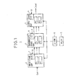
- FIG. 1 is a view of the basic configuration of a digital signal processor system according to the present invention.
- reference numeral 1 indicates a digital signal processor system comprised of at least three blocks (2, 3, and 4), that is, an input digital signal processor 2 arranged at an input side (Din) of data to be processed, an output digital signal processor 4 arranged at an output side (Dout) of processed data, and at least one intermediate digital signal processor 3 interposed between the input digital signal processor 2 and the output digital signal processor 4.
- the input digital signal processor 2, the intermediate digital signal processor 3, and the output digital signal processor 4 are connected in cascade in that order.
- the input digital signal processor 2, the intermediate digital signal processor 3, and the output digital signal processor 4 store their inherent programs (P1, P2, and P3) and an identical common program Pc shared by the digital signal processors.
- the inherent programs are programs for input of data and output of data in the input digital signal processor 2, the intermediate digital signal processor 3, and the output digital signal processor 4, while the common program Pc is a program for arithmetic/logic processing of the data at each of the input digital signal processor 2, the intermediate digital signal processor 3, and the output digital signal processor 4.
- the digital signal processor system 1 of this configuration preferably an FIR filter, fundamentally differs from the audio signal processor system disclosed in Japanese Unexamined Patent Publication (Kokai) No. 8-79879 providing FIR filters for respective frequency bandwidths.
- the digital signal processor system 1 shown in FIG. 1 further is provided with a microprocessor 5.
- the microprocessor 5 transfers the common program Pc and all the inherent programs (P1, P2, and P3) in its associated ROM to the input digital signal processor 2, the intermediate digital signal processor 3, and the output digital signal processor 4.
- the input digital signal processor 2, the intermediate digital signal processor 3, and the output digital signal processor 4 are driven by the common program Pc and the inherent programs (P1, P2, and P3) selected corresponding to the same.
- the input digital signal processor 2, the intermediate digital signal processor 3, and the output digital signal processor 4 are provided with respective I/O units (7, 8, and 9).
- the inherent programs (P1, P2, and P3) corresponding to the digital signal processors are autonomously selected based on identification information Id set for the I/O units from the outside.
- the input digital signal processor 2, the intermediate digital signal processor 3, and the output digital signal processor 4 are provided with respective identification registers for holding the set identification information Id.
- the input digital signal processor 2, the intermediate digital signal processor 3, and the output digital signal processor 4 form an FIR type digital filter for performing filtering which corresponds to the aforementioned arithmetic/logic processing.
- This FIR type digital filter will be explained in detail below.
- FIG. 2 is a schematic view of an audio player to which the present invention may be applied.
- the example of this figure shows a configuration for amplifying the output from a CD player (CDP) by an amplifier (AMP) and outputting the result to a speaker (SP).
- CDP CD player
- AMP amplifier
- SP speaker
- the amplifier in this configuration a little more in detail, it is comprised of a PRE stage and a POWER stage. Among these, the present invention is applied to the PRE stage.
- the PRE stage includes an FIR filter.
- FIG. 3 is a view of an FIR filter unit in the PRE stage in FIG. 2. Note that throughout the drawings, similar components are assigned the same reference numerals or symbols.
- reference numeral 10 indicates an FIR filter unit.
- the [INPUT] side corresponds to the CDP side in FIG. 2, while the [OUTPUT] side corresponds to the POWER stage side of FIG. 2.
- the components already explained in FIG. 1 are the digital signal processor system 1, the microprocessor 5, and the ROM 6 comprised of for example a flash memory.
- the input side of the digital signal processor system 1 is provided with an analog/digital converter (A/D) 11, while the output side is provided with a digital/analog converter (D/A) 12.
- These converters 11 and 12 and a digital interface receiver (DIR) constitute a codec 13.
- the digital interface receiver communicates with a built-in digital interface transmitter (DIT).
- the main part of the present invention is the FIR filter (digital signal processor system 1) shown in FIG. 3.
- FIG. 4 is a block diagram showing the digital signal processor system 1 (FIR filter) of FIG. 3 in more detail.
- reference numeral 21 indicates an FIR filter comprised of an input digital signal processor 22, at least one intermediate digital signal processor 23, and an output digital signal processor 24.
- These digital signal processors correspond to the digital signal processors 2, 3, and 4 shown in FIG. 1. Further, these digital signal processors 22, 23, and 24 are driven by the programs explained below.
- FIG. 5 is a view of the programs used for driving the digital signal processors in FIG. 4.
- the common program (d) is a program for the arithmetic and logic processing at the FIR filter 21, that is, filtering.
- FIG. 6 is a view of a typical example of the configuration of a general FIR filter. As will be understood from this figure, this FIR filter performs convolution (multiplying and accumulating) processing. This processing requires a considerable size of program and therefore requires a corresponding number of digital signal processors. Note that Z -1 indicates the unit delay, K1, K2... Kn indicate filter coefficients, and ACC indicates an accumulator.
- FIG. 7 is a view of the layout of the programs for driving digital signal processors loaded in the ROM.
- the group of programs comprised as shown in the figure are transferred from the microprocessor 5 of FIG. 3 to all of the digital signal processors 22, 23, and 24 and stored therein.
- the digital signal processor 22 selects the programs (a), (d), and (e)
- the digital signal processor 24 selects the programs (b), (d), and (f)
- the digital signal processor 23 selects the programs (c), (d), and (g). These are used for driving them.
- the digital signal processors (22, 23, and 24) select the programs autonomously. An example of the configuration for this will be explained below.
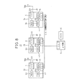
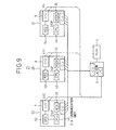
- FIG. 8 and FIG. 9 are views of the configuration of connections for communication between the digital signal processors and the microprocessor. Note that illustration of the lines for transfer of data is omitted.
- the group of programs (FIG. 7) transferred from the microprocessor 5 is stored in the memories (MEM) 32, 33, and 34 of the digital signal processors 22, 23, and 24.
- the central processing units (CPUs) 42, 43, and 44 in the digital signal processors 22, 23, and 24 select the corresponding programs (for example, in the case of the digital signal processor 22, as mentioned above, (a), (d), and (e)) from the group of programs stored in the memories (MEM) and start their processing.
- Which programs to select at this time is determined by the identification information Id2, Id3, and Id4 set at respective I/O units (I/O ports) 7, 8, and 9. In this figure, for example, it is determined by the voltage levels of the 5V VDD and ground. That is, it is determined by external hardware.
- R is a pull-up resistor.
- Id2 (1,0)
- Id3 (0,0)
- Id4 (0,1)
- the digital signal processor 22 autonomously selects the programs (a)+(d)+(e) since (1,0)
- the digital signal processor 23 selects the programs (c)+(d)+(g) since (0,0)
- the digital signal processor 24 selects the programs (b)+(d)+(f) since (0.1).
- identification registers (REG) 52, 53, and 54 are preferably provided with identification registers (REG) 52, 53, and 54 and the identification information held therein.
- the identification information Id2, Id3, and Id4 are set from the microprocessor 5 by software through respective I/O units (I/O ports) 7, 8, and 9. The specific operations will be explained below.
- FIG. 10 and FIG. 11 are parts of a flow chart of an example of operation in FIG. 8; and FIG. 12 and FIG. 13 are parts of a flow chart of an example of operation in FIG. 9.
- Step 11 The microprocessor 5 transfers the programs of FIG. 7.
- Step 12 The digital signal processor 22 receives the transferred programs.
- Step 13 The digital signal processor 22 checks that the programs are normally received. If yes, the routine proceeds to step S14.
- Step 14 The microprocessor 5 transfers the required filter coefficients to the digital signal processor 22.
- This filter coefficients referring for example to FIG. 3, are given to the microprocessor 5 as filter control information shown at the bottom left in that figure. For example, when the cut-off frequency is changed by user settings, the filter coefficients are changed accordingly.
- Step 15 The digital signal processor 22 receives the filter coefficients from the microprocessor 5, then returns an OK/NG response to the microprocessor 5.
- Step 16 If the response is OK, the microprocessor 5 ends the processing, while if the response is NG, it reexecutes the processing of step S14.
- Step 17 The digital signal processor 22 normally receiving the filter coefficients at step S15 checks the identification information Id2 set at the I/O unit (I/O port) 7 of the digital signal processor 22.
- Step 18 The digital signal processor 22 places the identification information in its identification register (REG) 52.
- the digital signal processor 22 is ready to start its inherent filtering in accordance with the programs (a)+(d)+(e) corresponding to it.
- the microprocessor 5 repeats exactly the same steps as the above (S11 to S18) for the next digital signal processor 23. When it finishes this, it finally repeats exactly the same steps for the digital signal processor 24.
- the digital signal processor 22, the digital signal processor 23, and the digital signal processor 24 become ready to start operating, whereupon the filtering inherent to the FIR filter 21 commences.
- FIG. 12 and FIG. 13 an operation similar to the operation in FIG. 10 and FIG. 11 is performed.
- the identification information is set based on the software shown in FIG. 9.
- Step 21 The microprocessor 5 transmits the content of the setting for the I/O port, that is, the identification information Id2 designated for the digital signal processor 22.
- Step 22 The digital signal processor 22 returns an OK or NG response to the microprocessor 5 indicating whether the identification information has been normally received at the I/O unit 7.
- Step 23 If the microprocessor 5 receives an OK response, the routine proceeds to step S24, while if the microprocessor 5 receives an NG response, it reexecutes the processing of step S21.
- Step 24 The identification information Id2 for the digital signal processor 22 is set in the I/O port.
Landscapes
- Engineering & Computer Science (AREA)
- Theoretical Computer Science (AREA)
- Software Systems (AREA)
- Physics & Mathematics (AREA)
- General Engineering & Computer Science (AREA)
- General Physics & Mathematics (AREA)
- Computer Hardware Design (AREA)
- Computing Systems (AREA)
- Signal Processing (AREA)
- Complex Calculations (AREA)
- Circuit For Audible Band Transducer (AREA)
Applications Claiming Priority (2)
| Application Number | Priority Date | Filing Date | Title |
|---|---|---|---|
| JP2002286839 | 2002-09-30 | ||
| JP2002286839A JP4222808B2 (ja) | 2002-09-30 | 2002-09-30 | Dsp装置 |
Publications (2)
| Publication Number | Publication Date |
|---|---|
| EP1408419A2 true EP1408419A2 (fr) | 2004-04-14 |
| EP1408419A3 EP1408419A3 (fr) | 2005-08-24 |
Family
ID=32025383
Family Applications (1)
| Application Number | Title | Priority Date | Filing Date |
|---|---|---|---|
| EP03255024A Withdrawn EP1408419A3 (fr) | 2002-09-30 | 2003-08-13 | Système de processeur de signaux numériques |
Country Status (5)
| Country | Link |
|---|---|
| US (1) | US20040064197A1 (fr) |
| EP (1) | EP1408419A3 (fr) |
| JP (1) | JP4222808B2 (fr) |
| KR (1) | KR100583655B1 (fr) |
| CN (1) | CN1278487C (fr) |
Families Citing this family (3)
| Publication number | Priority date | Publication date | Assignee | Title |
|---|---|---|---|---|
| US8081766B2 (en) * | 2006-03-06 | 2011-12-20 | Loud Technologies Inc. | Creating digital signal processing (DSP) filters to improve loudspeaker transient response |
| JP6474246B2 (ja) | 2014-12-09 | 2019-02-27 | ローム株式会社 | オーディオ信号処理回路、車載用オーディオ装置、オーディオコンポーネント装置、電子機器 |
| JP2024000852A (ja) | 2022-06-21 | 2024-01-09 | キヤノン株式会社 | プログラマブル信号処理回路及び当該回路用のプログラム |
Citations (3)
| Publication number | Priority date | Publication date | Assignee | Title |
|---|---|---|---|---|
| JPH0437212A (ja) | 1990-05-31 | 1992-02-07 | Victor Co Of Japan Ltd | Firディジタルフィルタ装置 |
| JPH0879879A (ja) | 1994-09-08 | 1996-03-22 | Victor Co Of Japan Ltd | オーディオ信号処理装置 |
| US5764986A (en) | 1990-10-31 | 1998-06-09 | International Business Machines Corp. | Method for loading secondary stations with a structure representing initial program load information to be sent in a computer communication system |
Family Cites Families (8)
| Publication number | Priority date | Publication date | Assignee | Title |
|---|---|---|---|---|
| JPS63216170A (ja) * | 1987-03-05 | 1988-09-08 | Mitsubishi Electric Corp | デイジタル信号処理プロセツサ |
| JP2639543B2 (ja) * | 1987-12-02 | 1997-08-13 | 日本ビクター株式会社 | デジタル・フィルタ装置 |
| US5075880A (en) * | 1988-11-08 | 1991-12-24 | Wadia Digital Corporation | Method and apparatus for time domain interpolation of digital audio signals |
| US5140543A (en) * | 1989-04-18 | 1992-08-18 | Victor Company Of Japan, Ltd. | Apparatus for digitally processing audio signal |
| JPH0468671A (ja) * | 1990-07-04 | 1992-03-04 | Toshiba Corp | デジタル映像信号処理装置 |
| US6330660B1 (en) * | 1999-10-25 | 2001-12-11 | Vxtel, Inc. | Method and apparatus for saturated multiplication and accumulation in an application specific signal processor |
| US7007117B2 (en) * | 2000-11-29 | 2006-02-28 | Palmone, Incorporated | Identifying a type of connection and selecting a corresponding form of an application |
| US6798421B2 (en) * | 2001-02-28 | 2004-09-28 | 3D Labs, Inc. Ltd. | Same tile method |
-
2002
- 2002-09-30 JP JP2002286839A patent/JP4222808B2/ja not_active Expired - Fee Related
-
2003
- 2003-08-12 US US10/639,383 patent/US20040064197A1/en not_active Abandoned
- 2003-08-13 EP EP03255024A patent/EP1408419A3/fr not_active Withdrawn
- 2003-08-26 KR KR1020030059217A patent/KR100583655B1/ko not_active Expired - Fee Related
- 2003-09-04 CN CNB031563422A patent/CN1278487C/zh not_active Expired - Fee Related
Patent Citations (3)
| Publication number | Priority date | Publication date | Assignee | Title |
|---|---|---|---|---|
| JPH0437212A (ja) | 1990-05-31 | 1992-02-07 | Victor Co Of Japan Ltd | Firディジタルフィルタ装置 |
| US5764986A (en) | 1990-10-31 | 1998-06-09 | International Business Machines Corp. | Method for loading secondary stations with a structure representing initial program load information to be sent in a computer communication system |
| JPH0879879A (ja) | 1994-09-08 | 1996-03-22 | Victor Co Of Japan Ltd | オーディオ信号処理装置 |
Also Published As
| Publication number | Publication date |
|---|---|
| KR20040028496A (ko) | 2004-04-03 |
| EP1408419A3 (fr) | 2005-08-24 |
| CN1278487C (zh) | 2006-10-04 |
| KR100583655B1 (ko) | 2006-05-26 |
| JP2004128650A (ja) | 2004-04-22 |
| US20040064197A1 (en) | 2004-04-01 |
| CN1489287A (zh) | 2004-04-14 |
| JP4222808B2 (ja) | 2009-02-12 |
Similar Documents
| Publication | Publication Date | Title |
|---|---|---|
| US6611220B1 (en) | Architecture for decimation algorithm | |
| US7221187B1 (en) | Programmable microcontroller architecture (mixed analog/digital) | |
| EP0905890A2 (fr) | Structure de filtre et méthode de filtrage | |
| JP2009514067A (ja) | 直列周辺インターフェースを使用するマルチチャンネルデータ転送のためのデータ構造及び回路 | |
| EP1408419A2 (fr) | Système de processeur de signaux numériques | |
| JPH082014B2 (ja) | 多段デジタル・フィルタ | |
| CN114448390A (zh) | 一种Biquad数字滤波器装置及实现方法 | |
| US5502664A (en) | Filter device including SRAM and EEPROM devices | |
| JP7820151B2 (ja) | オーディオ回路 | |
| JPH0479516A (ja) | 集積回路装置における遅延回路 | |
| US7605723B2 (en) | Circuits and methods for implementing mode selection in multiple-mode integrated circuits | |
| CN1672327B (zh) | 数据处理电路 | |
| EP1551101A1 (fr) | Filtre FIR à performance améliorée | |
| JPH0575394A (ja) | デイジタルフイルタ及びデイジタル信号処理システム | |
| JP3104982B2 (ja) | ディジタル信号プロセッサ | |
| CN108228480A (zh) | 一种数字滤波器及数据处理方法 | |
| US20040057321A1 (en) | Device for storage of multiport data, particularly for an arithmetic and logic unit of a digital signal processing processor | |
| JP6474246B2 (ja) | オーディオ信号処理回路、車載用オーディオ装置、オーディオコンポーネント装置、電子機器 | |
| JP2017122625A (ja) | データ収録装置 | |
| JP2010103928A (ja) | D/aコンバータ | |
| JPH01265715A (ja) | 2次元ディジタルフィルター | |
| JPH01222507A (ja) | ディジタルフィルター | |
| JP2018049029A (ja) | データ収録装置 | |
| JPH0567395A (ja) | メモリ回路 | |
| JPH06283970A (ja) | フィルタ回路 |
Legal Events
| Date | Code | Title | Description |
|---|---|---|---|
| PUAI | Public reference made under article 153(3) epc to a published international application that has entered the european phase |
Free format text: ORIGINAL CODE: 0009012 |
|
| 17P | Request for examination filed |
Effective date: 20030902 |
|
| AK | Designated contracting states |
Kind code of ref document: A2 Designated state(s): AT BE BG CH CY CZ DE DK EE ES FI FR GB GR HU IE IT LI LU MC NL PT RO SE SI SK TR |
|
| AX | Request for extension of the european patent |
Extension state: AL LT LV MK |
|
| PUAL | Search report despatched |
Free format text: ORIGINAL CODE: 0009013 |
|
| AK | Designated contracting states |
Kind code of ref document: A3 Designated state(s): AT BE BG CH CY CZ DE DK EE ES FI FR GB GR HU IE IT LI LU MC NL PT RO SE SI SK TR |
|
| AX | Request for extension of the european patent |
Extension state: AL LT LV MK |
|
| AKX | Designation fees paid |
Designated state(s): DE GB |
|
| 17Q | First examination report despatched |
Effective date: 20070509 |
|
| STAA | Information on the status of an ep patent application or granted ep patent |
Free format text: STATUS: THE APPLICATION IS DEEMED TO BE WITHDRAWN |
|
| 18D | Application deemed to be withdrawn |
Effective date: 20130301 |