EP1413965A2 - Test et modèle de la réponse d'un système - Google Patents
Test et modèle de la réponse d'un système Download PDFInfo
- Publication number
- EP1413965A2 EP1413965A2 EP03256574A EP03256574A EP1413965A2 EP 1413965 A2 EP1413965 A2 EP 1413965A2 EP 03256574 A EP03256574 A EP 03256574A EP 03256574 A EP03256574 A EP 03256574A EP 1413965 A2 EP1413965 A2 EP 1413965A2
- Authority
- EP
- European Patent Office
- Prior art keywords
- input
- maximum
- minimum
- input value
- response
- Prior art date
- Legal status (The legal status is an assumption and is not a legal conclusion. Google has not performed a legal analysis and makes no representation as to the accuracy of the status listed.)
- Withdrawn
Links
Images


Classifications
-
- G—PHYSICS
- G06—COMPUTING OR CALCULATING; COUNTING
- G06F—ELECTRIC DIGITAL DATA PROCESSING
- G06F11/00—Error detection; Error correction; Monitoring
- G06F11/07—Responding to the occurrence of a fault, e.g. fault tolerance
-
- G—PHYSICS
- G06—COMPUTING OR CALCULATING; COUNTING
- G06F—ELECTRIC DIGITAL DATA PROCESSING
- G06F30/00—Computer-aided design [CAD]
- G06F30/30—Circuit design
- G06F30/36—Circuit design at the analogue level
- G06F30/367—Design verification, e.g. using simulation, simulation program with integrated circuit emphasis [SPICE], direct methods or relaxation methods
Definitions
- the present invention relates generally to the field of system analysis, and in particular a system and method of system response testing and modeling.
- a method comprises exciting a system with a step input having predetermined maximum and minimum input values, selecting time points t i and t j in a system response having a plurality of maximum response values at time points t i and a plurality of minimum response values at time points t j .
- a maximum worst-case excitation input is then generated.
- the maximum worst-case excitation input has a positive transition from the predetermined minimum input value to the predetermined maximum input value at each time point (T - t i ), and a negative transition from the predetermined maximum input value to the predetermined minimum input value at each time point (T - t j ).
- a method comprises exciting a system with a worst-case excitation input.
- the worst-case excitation input is generated by selecting time points t i and t j in a standard system response to a standard input having a plurality of maximum response values at time points t i and a plurality of minimum response values at time points t j , the standard input having predetermined minimum and maximum input values.
- a maximum worst-case excitation input is generated, which has a positive transition from the predetermined minimum input value to the predetermined maximum input value at each time (T - t i ), and a negative transition from the predetermined maximum input value to the predetermined minimum input value at each time (T - t j ).
- a worst-case system response to the worst-case excitation input is then observed.
- a system comprises an interface to a target system, the interface operable to supply input to the target system and receive output from the target system, and a microprocessor coupled to the interface and operable to generate a worst-case excitation input.
- the worst-case excitation input is generated by: selecting time points t i and t j in a standard system response to a standard input having a plurality of maximum response values at time points t i and a plurality of minimum response values at time points t j , the standard input having predetermined minimum and maximum input values, and generating a maximum worst-case excitation waveform having a positive transition from the predetermined minimum input value to the predetermined maximum input value at each time (T - t i ), and a negative transition from the predetermined maximum input value to the predetermined minimum input value at each time (T - t j ).
- a system comprising a computer-executable medium having encoded thereon a process.
- the process is operable to excite a system with a step input having predetermined maximum and minimum input values, select time points t i and t j in a system response having a plurality of maximum response values at time points ti and a plurality of minimum response values at time points t j , and generate a maximum worst-case excitation input having a positive transition from the predetermined minimum input value to the predetermined maximum input value at each time point (T - t i ), and a negative transition from the predetermined maximum input value to the predetermined minimum input value at each time point (T - t j ).
- FIGURE 1 is a simplified block diagram illustrating an embodiment of the present invention
- FIGURE 2 is a flowchart of an embodiment of a method of determining the maximum system response according to the teachings of the present invention
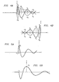
- FIGURES 3A and 3B are a plots of an exemplary stimulus current and standard voltage response, respectively, according to the teachings of the present invention.
- FIGURE 4A is a plot of an exemplary shifting of standard voltage response to construct the stimulus input according to the teachings of the present invention.
- FIGURE 4B is a plot of an exemplary system response waveform in reverse time order
- FIGURES 5A through 5D are plots of exemplary shifted voltage responses by t i or t j according to the teachings of the present invention.
- FIGURE 6 is a plot of an exemplary input stimulus current operable to induce a worst-case voltage response according to the teachings of the present invention
- FIGURE 7 is a plot of an exemplary stimulus current and inverse standard stimulus current according to the teachings of the present invention.
- FIGURE 8 is a plot of an exemplary standard voltage response and inverse standard voltage response according to the teachings of the present invention.
- FIGURE 9 is a plot of an exemplary worst case minimum voltage and stimulus current according to the teachings of the present invention.
- FIGURE 10 is a plot of an exemplary worst-case maximum voltage and stimulus current according to the teachings of the present invention.
- FIGURES 1 through 10 of the drawings like numerals being used for like and corresponding parts of the various drawings.
- FIGURE 1 is a simplified block diagram illustrating an embodiment of the present invention.
- the present invention is applicable to mechanical or electrical systems.
- a system 10 receives an input as a function of time, such as I(t).
- the input may be unevenness in the road for an automotive suspension system, for example, or the input current of an electrical/electronic circuit such as a microprocessor.
- the output or system response to the input as a function of time is V(t). It is of interest to system designers to determine whether system 10 is able to function properly when it is subjected to an input that subjects system 10 to the maximum excitation.
- FIGURE 2 is a flowchart of an embodiment of a method 12 of determining the input that would create the maximum system response according to the teachings of the present invention.
- System 10 is first subject to a step input.
- FIGURE 3 is an exemplary plot of a step current function having a high current level at t ⁇ 0 and at a low current level at t > 0.
- this input may be some standard input or excitation that would generate a measurable system response. Note that there is some finite time during which the time the current level transitions from high to low levels.
- FIGURE 3 further shows a voltage step response to the input current. The points in time, t 0 , t 1 , t 2 , t 3 ,...,where local maxima (V 0 and V 2 , for example, as shown in FIGURE 3) and minima (V 1 and V 3 , for example) responses occur are noted, as shown in blocks 14 and 16 of FIGURE 2. The maxima and minima time occurrences are noted until V(t) tapers to insignificant or unimportant measurements. The occurrences of the maximum points should alternate with the minimum points. In other words, there is only one maximum between any two adjacent minimum points, and there is only one minimum between any two adjacent maximum points.
- a time, T is chosen that is equal or later in time than the maximum of time points t 0 , t 1 , t 2 , t 3 ,....
- the worst-case stimuli is defined as the input that results in maximum or minimum response value.
- the positive and negative voltage step responses can be shifted by shifting the positive and negative input current transients so. that the worst-case voltage response occurs at T, as seen in FIGURE 4.
- a shift of the voltage step response by -to is made, and an input at the maximum input value is determined, as shown in FIGURE 5A.
- FIGURE 5B a shift of the negative or inverse voltage step response by -t 1 is made.
- FIGURE 5C a shift of the voltage step response by -t 2 is made.
- FIGURE 5D a shift of the negative voltage step response by -t 3 is made.
- FIGURE 5E shows a composite plot of all the shifted voltage step response and negative voltage step responses. At time T, the worst-case system response would occur.
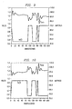
- FIGURE 7 a plot of an exemplary standard stimulus current and inverse standard stimulus current plotted by a circuit simulation software.
- FIGURE 8 is a plot of an exemplary standard voltage response and inverse standard voltage response, V(t).
- FIGURE 9 is a plot of an exemplary worst case minimum voltage and stimulus current according to the teachings of the present invention, and
- FIGURE 10 is a plot of an exemplary worst case maximum voltage and stimulus current according to the teachings of the present invention.
- the method of the present invention is operable to determine the input excitation that would induce the maximum and minimum response in the target system. In test conditions the stimulus input is maintained within its maximum and minimum bounds while the waveform is random.
- the present invention has been described with respect to electrical or electronic systems, the present invention is also applicable to mechanical systems such as automotive suspension systems, for example, where it is of interest to subject the system to an input that would create the worst-case response to verify the system design and operations.
- the unit step input for a suspension system may be a bump of a predetermined height, such as five inches.
- the system response would be the amount of deviation from neutral in the upward and downward directions, and the times t i for maximum deviation in the upward direction and times t j for maximum deviation in the downward direction. It may be seen that the present invention may be modified and adapted to the testing and modeling of other types of systems either in a laboratory or in a simulated model.
- the present invention may be embodied in a test system or simulation system that first determines the worst-case excitation input of the target system, and then subjects the target system to the worst-case excitation input. Again, the system may test the actual system or simulate the testing with a model of the system.
- a test system or simulation system that first determines the worst-case excitation input of the target system, and then subjects the target system to the worst-case excitation input.
- the system may test the actual system or simulate the testing with a model of the system.
- Such a system is likely to be microprocessor-based and have an interface that is operable to supply the excitation input to the system being tested and to receive output from the system.
Landscapes
- Engineering & Computer Science (AREA)
- Computer Hardware Design (AREA)
- Theoretical Computer Science (AREA)
- Physics & Mathematics (AREA)
- General Engineering & Computer Science (AREA)
- General Physics & Mathematics (AREA)
- Geometry (AREA)
- Evolutionary Computation (AREA)
- Microelectronics & Electronic Packaging (AREA)
- Quality & Reliability (AREA)
- Tests Of Electronic Circuits (AREA)
- Test And Diagnosis Of Digital Computers (AREA)
- Management, Administration, Business Operations System, And Electronic Commerce (AREA)
- Vehicle Body Suspensions (AREA)
Applications Claiming Priority (2)
| Application Number | Priority Date | Filing Date | Title |
|---|---|---|---|
| US10/274,712 US20040078183A1 (en) | 2002-10-21 | 2002-10-21 | System and method of system response testing and modeling |
| US274712 | 2002-10-21 |
Publications (2)
| Publication Number | Publication Date |
|---|---|
| EP1413965A2 true EP1413965A2 (fr) | 2004-04-28 |
| EP1413965A3 EP1413965A3 (fr) | 2004-12-08 |
Family
ID=32069294
Family Applications (1)
| Application Number | Title | Priority Date | Filing Date |
|---|---|---|---|
| EP03256574A Withdrawn EP1413965A3 (fr) | 2002-10-21 | 2003-10-17 | Test et modèle de la réponse d'un système |
Country Status (6)
| Country | Link |
|---|---|
| US (1) | US20040078183A1 (fr) |
| EP (1) | EP1413965A3 (fr) |
| JP (1) | JP2004145882A (fr) |
| KR (1) | KR20040034533A (fr) |
| IL (1) | IL155929A (fr) |
| TW (1) | TWI223198B (fr) |
Cited By (1)
| Publication number | Priority date | Publication date | Assignee | Title |
|---|---|---|---|---|
| CN110096750A (zh) * | 2019-04-02 | 2019-08-06 | 燕山大学 | 考虑非线性主动悬架执行器的自适应动态面控制方法 |
Family Cites Families (18)
| Publication number | Priority date | Publication date | Assignee | Title |
|---|---|---|---|---|
| US4924430A (en) * | 1988-01-28 | 1990-05-08 | Teradyne, Inc. | Static timing analysis of semiconductor digital circuits |
| JPH06276039A (ja) * | 1993-03-17 | 1994-09-30 | Sanyo Electric Co Ltd | 高周波回路の設計方法 |
| JP3727103B2 (ja) * | 1996-04-05 | 2005-12-14 | 三菱電機株式会社 | 半導体素子の試験方法 |
| US6049219A (en) * | 1996-05-13 | 2000-04-11 | The United States Of America As Represented By The Secretary Of The Air Force | Signal probing of microwave integrated circuit internal nodes |
| US6185723B1 (en) * | 1996-11-27 | 2001-02-06 | International Business Machines Corporation | Method for performing timing analysis of a clock-shaping circuit |
| BR9909905B1 (pt) * | 1998-04-03 | 2012-12-11 | operador para uma chave aérea de energia elétrica e método de operação de uma chave de energia elétrica aérea. | |
| US6567773B1 (en) * | 1999-11-17 | 2003-05-20 | International Business Machines Corporation | Use of static noise analysis for integrated circuits fabricated in a silicon-on-insulator process technology |
| JP2001208803A (ja) * | 2000-01-24 | 2001-08-03 | Advantest Corp | 半導体集積回路の故障シミュレーション方法および故障シミュレータ |
| US6518782B1 (en) * | 2000-08-29 | 2003-02-11 | Delta Design, Inc. | Active power monitoring using externally located current sensors |
| JP2002110489A (ja) * | 2000-09-26 | 2002-04-12 | Toshiba Corp | 半導体装置の回路特性のシミュレータ、及び、シミュレート方法 |
| US6442741B1 (en) * | 2000-10-06 | 2002-08-27 | Lsi Logic Corporation | Method of automatically generating schematic and waveform diagrams for analysis of timing margins and signal skews of relevant logic cells using input signal predictors and transition times |
| US6472899B2 (en) * | 2000-12-29 | 2002-10-29 | Intel Corporation | Method for determining a load line based variable voltage input for an integrated circuit product |
| US6665843B2 (en) * | 2001-01-20 | 2003-12-16 | International Business Machines Corporation | Method and system for quantifying the integrity of an on-chip power supply network |
| US6564365B1 (en) * | 2001-08-03 | 2003-05-13 | Hewlett-Packard Development Company, L.P. | Method of simultaneously displaying schematic and timing data |
| US7062734B2 (en) * | 2002-04-05 | 2006-06-13 | Collins Jr Truman Wesley | Slack time analysis through latches on a circuit design |
| US7840803B2 (en) * | 2002-04-16 | 2010-11-23 | Massachusetts Institute Of Technology | Authentication of integrated circuits |
| US7155691B2 (en) * | 2003-06-06 | 2006-12-26 | Nascentric, Inc. | Apparatus and methods for compiled static timing analysis |
| US7102357B2 (en) * | 2004-03-22 | 2006-09-05 | Hewlett-Packard Development Company, L.P. | Determination of worst case voltage in a power supply loop |
-
2002
- 2002-10-21 US US10/274,712 patent/US20040078183A1/en not_active Abandoned
-
2003
- 2003-05-15 IL IL155929A patent/IL155929A/en not_active IP Right Cessation
- 2003-05-20 TW TW092113582A patent/TWI223198B/zh not_active IP Right Cessation
- 2003-10-09 JP JP2003350743A patent/JP2004145882A/ja not_active Withdrawn
- 2003-10-17 EP EP03256574A patent/EP1413965A3/fr not_active Withdrawn
- 2003-10-20 KR KR1020030072838A patent/KR20040034533A/ko not_active Withdrawn
Cited By (2)
| Publication number | Priority date | Publication date | Assignee | Title |
|---|---|---|---|---|
| CN110096750A (zh) * | 2019-04-02 | 2019-08-06 | 燕山大学 | 考虑非线性主动悬架执行器的自适应动态面控制方法 |
| CN110096750B (zh) * | 2019-04-02 | 2020-12-11 | 燕山大学 | 考虑非线性主动悬架执行器的自适应动态面控制方法 |
Also Published As
| Publication number | Publication date |
|---|---|
| JP2004145882A (ja) | 2004-05-20 |
| KR20040034533A (ko) | 2004-04-28 |
| US20040078183A1 (en) | 2004-04-22 |
| TWI223198B (en) | 2004-11-01 |
| IL155929A0 (en) | 2003-12-23 |
| IL155929A (en) | 2006-08-20 |
| TW200406706A (en) | 2004-05-01 |
| EP1413965A3 (fr) | 2004-12-08 |
Similar Documents
| Publication | Publication Date | Title |
|---|---|---|
| EP3936877B1 (fr) | Instrument de mesure, système de mesure et procédé de traitement de signal | |
| EP2345905A2 (fr) | Évaluateur de caractéristiques de batterie | |
| US20040049750A1 (en) | Process and system for identifying wires at risk of electromigration | |
| US20040078175A1 (en) | Method and apparatus for modeling and simulating the effects of bridge defects in integrated circuits | |
| JP4500338B2 (ja) | テストパターン評価方法及びテストパターン評価装置 | |
| US6795802B2 (en) | Apparatus and method for calculating temporal deterioration margin amount of LSI, and LSI inspection method | |
| US20050024064A1 (en) | System and method for testing devices | |
| EP1413965A2 (fr) | Test et modèle de la réponse d'un système | |
| EP0590575A1 (fr) | Circuit de commande de test pour trajet d'analyse | |
| US20080155484A1 (en) | System and method for memory element characterization | |
| US6934670B2 (en) | Virtual test environment | |
| JP4600823B2 (ja) | 電子回路解析プログラム、方法及び装置 | |
| CN114355161B (zh) | 互联状态在线监测电路及方法 | |
| Stievano et al. | Behavioral models of digital IC ports from measured transient waveforms | |
| US20060190872A1 (en) | System and method for signal integrity testing of electronic circuits | |
| Gunther | A proposed flicker meter test protocol | |
| JP4295894B2 (ja) | 半導体デバイスの試験装置および試験方法 | |
| US20040002847A1 (en) | Method for creating and displaying signaling eye-plots | |
| EP3786651B1 (fr) | Procédé et dispositif de fourniture d'un modèle de comportement pour la simulation des émissions d'interférence électromagnétique d'un composant électrique ou électronique | |
| JP2003030270A (ja) | 同期式順序回路のプロパティ検証方法および装置 | |
| EP0853280A2 (fr) | Procédé et appareil de verification temporelle | |
| JP2624135B2 (ja) | タイミング解析方法 | |
| CN119667438A (zh) | 一种risc-v dsp芯片测试波形自动生成方法、系统和存储介质 | |
| JP3123982B2 (ja) | 論理シミュレーション方法 | |
| Doyle et al. | Techniques and considerations for verification of model causality |
Legal Events
| Date | Code | Title | Description |
|---|---|---|---|
| PUAI | Public reference made under article 153(3) epc to a published international application that has entered the european phase |
Free format text: ORIGINAL CODE: 0009012 |
|
| AK | Designated contracting states |
Kind code of ref document: A2 Designated state(s): AT BE BG CH CY CZ DE DK EE ES FI FR GB GR HU IE IT LI LU MC NL PT RO SE SI SK TR |
|
| AX | Request for extension of the european patent |
Extension state: AL LT LV MK |
|
| PUAL | Search report despatched |
Free format text: ORIGINAL CODE: 0009013 |
|
| AK | Designated contracting states |
Kind code of ref document: A3 Designated state(s): AT BE BG CH CY CZ DE DK EE ES FI FR GB GR HU IE IT LI LU MC NL PT RO SE SI SK TR |
|
| AX | Request for extension of the european patent |
Extension state: AL LT LV MK |
|
| 17P | Request for examination filed |
Effective date: 20050606 |
|
| AKX | Designation fees paid |
Designated state(s): DE FR GB IT |
|
| STAA | Information on the status of an ep patent application or granted ep patent |
Free format text: STATUS: THE APPLICATION IS DEEMED TO BE WITHDRAWN |
|
| 18D | Application deemed to be withdrawn |
Effective date: 20080503 |