EP1414029A2 - Support d'enregistrement optique et son procédé de fabrication - Google Patents
Support d'enregistrement optique et son procédé de fabrication Download PDFInfo
- Publication number
- EP1414029A2 EP1414029A2 EP20030023871 EP03023871A EP1414029A2 EP 1414029 A2 EP1414029 A2 EP 1414029A2 EP 20030023871 EP20030023871 EP 20030023871 EP 03023871 A EP03023871 A EP 03023871A EP 1414029 A2 EP1414029 A2 EP 1414029A2
- Authority
- EP
- European Patent Office
- Prior art keywords
- dielectric layer
- layer
- recording
- primary component
- recording medium
- Prior art date
- Legal status (The legal status is an assumption and is not a legal conclusion. Google has not performed a legal analysis and makes no representation as to the accuracy of the status listed.)
- Withdrawn
Links
- 230000003287 optical effect Effects 0.000 title claims abstract description 136
- 238000000034 method Methods 0.000 title claims abstract description 32
- 238000004519 manufacturing process Methods 0.000 title claims abstract description 15
- IJGRMHOSHXDMSA-UHFFFAOYSA-N Atomic nitrogen Chemical compound N#N IJGRMHOSHXDMSA-UHFFFAOYSA-N 0.000 claims abstract description 253
- 229910052757 nitrogen Inorganic materials 0.000 claims abstract description 123
- 239000007789 gas Substances 0.000 claims abstract description 31
- 229910001873 dinitrogen Inorganic materials 0.000 claims abstract description 9
- 239000012298 atmosphere Substances 0.000 claims abstract description 3
- 238000001947 vapour-phase growth Methods 0.000 claims abstract description 3
- GWEVSGVZZGPLCZ-UHFFFAOYSA-N Titan oxide Chemical compound O=[Ti]=O GWEVSGVZZGPLCZ-UHFFFAOYSA-N 0.000 claims description 70
- 239000000654 additive Substances 0.000 claims description 38
- 230000000996 additive effect Effects 0.000 claims description 35
- PBCFLUZVCVVTBY-UHFFFAOYSA-N tantalum pentoxide Inorganic materials O=[Ta](=O)O[Ta](=O)=O PBCFLUZVCVVTBY-UHFFFAOYSA-N 0.000 claims description 32
- 229910052782 aluminium Inorganic materials 0.000 claims description 22
- 238000004544 sputter deposition Methods 0.000 claims description 21
- 229910052802 copper Inorganic materials 0.000 claims description 18
- 229910052718 tin Inorganic materials 0.000 claims description 18
- 229910052710 silicon Inorganic materials 0.000 claims description 17
- 230000008569 process Effects 0.000 claims description 16
- 229910052725 zinc Inorganic materials 0.000 claims description 16
- 229910052749 magnesium Inorganic materials 0.000 claims description 13
- 229910052719 titanium Inorganic materials 0.000 claims description 13
- 229910052732 germanium Inorganic materials 0.000 claims description 12
- 229910052737 gold Inorganic materials 0.000 claims description 10
- 229910052709 silver Inorganic materials 0.000 claims description 8
- 229910052799 carbon Inorganic materials 0.000 claims description 5
- 229910052738 indium Inorganic materials 0.000 claims description 5
- 229910052763 palladium Inorganic materials 0.000 claims description 5
- 229910052797 bismuth Inorganic materials 0.000 claims description 3
- 239000010410 layer Substances 0.000 description 439
- 230000008033 biological extinction Effects 0.000 description 69
- 239000000758 substrate Substances 0.000 description 44
- 230000005540 biological transmission Effects 0.000 description 28
- 229920005989 resin Polymers 0.000 description 20
- 239000011347 resin Substances 0.000 description 20
- 230000035945 sensitivity Effects 0.000 description 18
- 230000003247 decreasing effect Effects 0.000 description 17
- 239000000463 material Substances 0.000 description 15
- 239000004417 polycarbonate Substances 0.000 description 12
- 229920000515 polycarbonate Polymers 0.000 description 12
- 238000004833 X-ray photoelectron spectroscopy Methods 0.000 description 11
- 230000007423 decrease Effects 0.000 description 11
- 239000010936 titanium Substances 0.000 description 11
- 239000011247 coating layer Substances 0.000 description 10
- 238000003860 storage Methods 0.000 description 10
- 239000012071 phase Substances 0.000 description 9
- XKRFYHLGVUSROY-UHFFFAOYSA-N Argon Chemical compound [Ar] XKRFYHLGVUSROY-UHFFFAOYSA-N 0.000 description 8
- 238000002425 crystallisation Methods 0.000 description 7
- 230000008025 crystallization Effects 0.000 description 7
- 238000005259 measurement Methods 0.000 description 7
- 229910018321 SbTe Inorganic materials 0.000 description 6
- NIXOWILDQLNWCW-UHFFFAOYSA-N acrylic acid group Chemical group C(C=C)(=O)O NIXOWILDQLNWCW-UHFFFAOYSA-N 0.000 description 6
- 238000001746 injection moulding Methods 0.000 description 5
- 230000007774 longterm Effects 0.000 description 5
- 239000012782 phase change material Substances 0.000 description 5
- 238000004528 spin coating Methods 0.000 description 5
- 229910052786 argon Inorganic materials 0.000 description 4
- QVGXLLKOCUKJST-UHFFFAOYSA-N atomic oxygen Chemical compound [O] QVGXLLKOCUKJST-UHFFFAOYSA-N 0.000 description 4
- 239000013626 chemical specie Substances 0.000 description 4
- 239000000203 mixture Substances 0.000 description 4
- 229910052760 oxygen Inorganic materials 0.000 description 4
- 239000001301 oxygen Substances 0.000 description 4
- 230000008859 change Effects 0.000 description 3
- 229910052804 chromium Inorganic materials 0.000 description 3
- 230000001747 exhibiting effect Effects 0.000 description 3
- 229910052742 iron Inorganic materials 0.000 description 3
- 229910052698 phosphorus Inorganic materials 0.000 description 3
- 229910052715 tantalum Inorganic materials 0.000 description 3
- 238000002834 transmittance Methods 0.000 description 3
- 239000004925 Acrylic resin Substances 0.000 description 2
- 229920000178 Acrylic resin Polymers 0.000 description 2
- 239000004593 Epoxy Substances 0.000 description 2
- RTAQQCXQSZGOHL-UHFFFAOYSA-N Titanium Chemical compound [Ti] RTAQQCXQSZGOHL-UHFFFAOYSA-N 0.000 description 2
- 230000015572 biosynthetic process Effects 0.000 description 2
- 239000013078 crystal Substances 0.000 description 2
- 230000001678 irradiating effect Effects 0.000 description 2
- 238000010030 laminating Methods 0.000 description 2
- 229920005668 polycarbonate resin Polymers 0.000 description 2
- 239000004431 polycarbonate resin Substances 0.000 description 2
- 229920005672 polyolefin resin Polymers 0.000 description 2
- 239000011241 protective layer Substances 0.000 description 2
- 229910052761 rare earth metal Inorganic materials 0.000 description 2
- 239000000243 solution Substances 0.000 description 2
- 239000002904 solvent Substances 0.000 description 2
- GUVRBAGPIYLISA-UHFFFAOYSA-N tantalum atom Chemical compound [Ta] GUVRBAGPIYLISA-UHFFFAOYSA-N 0.000 description 2
- 229910000967 As alloy Inorganic materials 0.000 description 1
- 239000004743 Polypropylene Substances 0.000 description 1
- XECAHXYUAAWDEL-UHFFFAOYSA-N acrylonitrile butadiene styrene Chemical compound C=CC=C.C=CC#N.C=CC1=CC=CC=C1 XECAHXYUAAWDEL-UHFFFAOYSA-N 0.000 description 1
- 239000004676 acrylonitrile butadiene styrene Substances 0.000 description 1
- 229920000122 acrylonitrile butadiene styrene Polymers 0.000 description 1
- 239000000853 adhesive Substances 0.000 description 1
- 229910045601 alloy Inorganic materials 0.000 description 1
- 239000000956 alloy Substances 0.000 description 1
- 229910052787 antimony Inorganic materials 0.000 description 1
- 230000015556 catabolic process Effects 0.000 description 1
- 239000000919 ceramic Substances 0.000 description 1
- 230000000052 comparative effect Effects 0.000 description 1
- 238000006731 degradation reaction Methods 0.000 description 1
- 230000000593 degrading effect Effects 0.000 description 1
- 230000000694 effects Effects 0.000 description 1
- 238000010894 electron beam technology Methods 0.000 description 1
- 239000003822 epoxy resin Substances 0.000 description 1
- 239000004811 fluoropolymer Substances 0.000 description 1
- 229920002313 fluoropolymer Polymers 0.000 description 1
- 239000011521 glass Substances 0.000 description 1
- 229910052748 manganese Inorganic materials 0.000 description 1
- 230000008018 melting Effects 0.000 description 1
- 238000002844 melting Methods 0.000 description 1
- 229910052751 metal Inorganic materials 0.000 description 1
- 239000002184 metal Substances 0.000 description 1
- 239000007769 metal material Substances 0.000 description 1
- 150000002739 metals Chemical class 0.000 description 1
- 238000012986 modification Methods 0.000 description 1
- 230000004048 modification Effects 0.000 description 1
- 229910052759 nickel Inorganic materials 0.000 description 1
- 229910052697 platinum Inorganic materials 0.000 description 1
- 229920000647 polyepoxide Polymers 0.000 description 1
- 229920013716 polyethylene resin Polymers 0.000 description 1
- -1 polypropylene Polymers 0.000 description 1
- 229920001155 polypropylene Polymers 0.000 description 1
- 229920005990 polystyrene resin Polymers 0.000 description 1
- 230000009467 reduction Effects 0.000 description 1
- 229920002050 silicone resin Polymers 0.000 description 1
- 229910052714 tellurium Inorganic materials 0.000 description 1
- 229920002803 thermoplastic polyurethane Polymers 0.000 description 1
- 229910052721 tungsten Inorganic materials 0.000 description 1
- 238000001771 vacuum deposition Methods 0.000 description 1
- 229910052720 vanadium Inorganic materials 0.000 description 1
Images


Classifications
-
- G—PHYSICS
- G11—INFORMATION STORAGE
- G11B—INFORMATION STORAGE BASED ON RELATIVE MOVEMENT BETWEEN RECORD CARRIER AND TRANSDUCER
- G11B7/00—Recording or reproducing by optical means, e.g. recording using a thermal beam of optical radiation by modifying optical properties or the physical structure, reproducing using an optical beam at lower power by sensing optical properties; Record carriers therefor
- G11B7/24—Record carriers characterised by shape, structure or physical properties, or by the selection of the material
- G11B7/241—Record carriers characterised by shape, structure or physical properties, or by the selection of the material characterised by the selection of the material
- G11B7/252—Record carriers characterised by shape, structure or physical properties, or by the selection of the material characterised by the selection of the material of layers other than recording layers
- G11B7/257—Record carriers characterised by shape, structure or physical properties, or by the selection of the material characterised by the selection of the material of layers other than recording layers of layers having properties involved in recording or reproduction, e.g. optical interference layers or sensitising layers or dielectric layers, which are protecting the recording layers
- G11B7/2578—Record carriers characterised by shape, structure or physical properties, or by the selection of the material characterised by the selection of the material of layers other than recording layers of layers having properties involved in recording or reproduction, e.g. optical interference layers or sensitising layers or dielectric layers, which are protecting the recording layers consisting essentially of inorganic materials
-
- G—PHYSICS
- G11—INFORMATION STORAGE
- G11B—INFORMATION STORAGE BASED ON RELATIVE MOVEMENT BETWEEN RECORD CARRIER AND TRANSDUCER
- G11B7/00—Recording or reproducing by optical means, e.g. recording using a thermal beam of optical radiation by modifying optical properties or the physical structure, reproducing using an optical beam at lower power by sensing optical properties; Record carriers therefor
- G11B7/24—Record carriers characterised by shape, structure or physical properties, or by the selection of the material
- G11B7/2403—Layers; Shape, structure or physical properties thereof
- G11B7/24067—Combinations of two or more layers with specific interrelation
-
- G—PHYSICS
- G11—INFORMATION STORAGE
- G11B—INFORMATION STORAGE BASED ON RELATIVE MOVEMENT BETWEEN RECORD CARRIER AND TRANSDUCER
- G11B7/00—Recording or reproducing by optical means, e.g. recording using a thermal beam of optical radiation by modifying optical properties or the physical structure, reproducing using an optical beam at lower power by sensing optical properties; Record carriers therefor
- G11B7/24—Record carriers characterised by shape, structure or physical properties, or by the selection of the material
- G11B7/2403—Layers; Shape, structure or physical properties thereof
- G11B7/24035—Recording layers
-
- G—PHYSICS
- G11—INFORMATION STORAGE
- G11B—INFORMATION STORAGE BASED ON RELATIVE MOVEMENT BETWEEN RECORD CARRIER AND TRANSDUCER
- G11B7/00—Recording or reproducing by optical means, e.g. recording using a thermal beam of optical radiation by modifying optical properties or the physical structure, reproducing using an optical beam at lower power by sensing optical properties; Record carriers therefor
- G11B7/24—Record carriers characterised by shape, structure or physical properties, or by the selection of the material
- G11B7/241—Record carriers characterised by shape, structure or physical properties, or by the selection of the material characterised by the selection of the material
- G11B7/242—Record carriers characterised by shape, structure or physical properties, or by the selection of the material characterised by the selection of the material of recording layers
- G11B7/243—Record carriers characterised by shape, structure or physical properties, or by the selection of the material characterised by the selection of the material of recording layers comprising inorganic materials only, e.g. ablative layers
-
- G—PHYSICS
- G11—INFORMATION STORAGE
- G11B—INFORMATION STORAGE BASED ON RELATIVE MOVEMENT BETWEEN RECORD CARRIER AND TRANSDUCER
- G11B7/00—Recording or reproducing by optical means, e.g. recording using a thermal beam of optical radiation by modifying optical properties or the physical structure, reproducing using an optical beam at lower power by sensing optical properties; Record carriers therefor
- G11B7/24—Record carriers characterised by shape, structure or physical properties, or by the selection of the material
- G11B7/26—Apparatus or processes specially adapted for the manufacture of record carriers
- G11B7/266—Sputtering or spin-coating layers
-
- G—PHYSICS
- G11—INFORMATION STORAGE
- G11B—INFORMATION STORAGE BASED ON RELATIVE MOVEMENT BETWEEN RECORD CARRIER AND TRANSDUCER
- G11B7/00—Recording or reproducing by optical means, e.g. recording using a thermal beam of optical radiation by modifying optical properties or the physical structure, reproducing using an optical beam at lower power by sensing optical properties; Record carriers therefor
- G11B7/24—Record carriers characterised by shape, structure or physical properties, or by the selection of the material
- G11B7/2403—Layers; Shape, structure or physical properties thereof
- G11B7/24035—Recording layers
- G11B7/24038—Multiple laminated recording layers
Definitions
- the present invention relates to an optical recording medium and a method for manufacturing the same and, in particular, to an optical recording medium which exhibits excellent optical characteristics with respect to a laser beam of desired wavelength used for recording data and reproducing data, and a method for manufacturing the same.
- optical recording media such as the CD, DVD and the like have been widely used as recording media for recording digital data.
- These optical recording media can be roughly classified into optical recording media such as the CD-ROM and the DVD-ROM that do not enable writing and rewriting of data (ROM type optical recording media), optical recording media such as the CD-R and DVD-R that enable writing but not rewriting of data (write-once type optical recording media), and optical recording media such as the CD-RW and DVD-RW that enable rewriting of data (data rewritable type optical recording media).
- Data are ordinarily recorded in the ROM type optical recording medium using spirally formed pits formed in the medium substrate in the manufacturing process and data are reproduced from the medium by projecting a laser beam to pass along the spirally formed pits and detecting the amount of the reflected laser beam.
- the write-once type optical recording medium and data rewritable type optical recording medium are constituted to record data therein by projecting a laser beam whose intensity is modulated onto a recording layer of the medium containing an organic dye or a phase change material so as to pass along a groove and/or land spirally formed on a substrate of the medium, thereby chemically and/or physically changing the organic dye or the phase change material to form record marks, and to reproduce data therefrom by projecting a laser beam onto the recording layer to pass along the spirally formed groove and/or land and detecting the amount of the reflected laser beam.
- a dielectric layer is generally formed in the vicinity of the recording layer, ordinarily adjacent to the recording layer, for chemically and/or physically protecting the recording layer and increasing modulation, namely, the difference between the reflection coefficient of regions of the recording layer where record marks are formed and that of regions thereof where record marks are not formed.
- the dielectric layer In the case where a dielectric layer is formed in the vicinity of the recording layer in this manner, it is preferable for the dielectric layer to have a high refractive index n for increasing modulation, namely, the difference between the reflection coefficients of a region of the recording layer where a record mark is formed and a region thereof where no record mark is formed, and it is preferable for the dielectric layer to have a low extinction coefficient k for decreasing the energy of a laser beam absorbed in the dielectric layer, thereby improving the recording sensitivity and preventing the reflection coefficient from being lowered.
- n refractive index
- the refractive index n and the extinction coefficient k of a conventional dielectric layer greatly depend on the wavelength of the incident light, the refractive index n of the dielectric layer becomes low or the extinction coefficient k of the dielectric layer becomes high depending upon the wavelength of the laser beam used for recording and reproducing data and, as a result, the optical characteristics of the optical recording medium are sometimes degraded.
- the extinction coefficients k of some oxides among the oxides widely used for forming dielectric layers become higher with shorter laser beam wavelength and, therefore, if a dielectric layer is formed of such an oxide in a next-generation type optical recording medium in which data are recorded and reproduced using a laser beam in the blue wavelength band, it will be impossible to obtain excellent optical characteristics, namely, high modulation and high recording sensitivity.
- an object of the present invention is to provide an optical recording medium which exhibits excellent optical characteristics with respect to a laser beam of desired wavelength used for recording data and reproducing data, and a method for manufacturing the same.
- It is another object of the present invention is to provide an optical recording medium which exhibits excellent optical characteristics with respect to a laser beam in the blue wavelength band used for recording data and reproducing data and a method for manufacturing the same.
- the inventors of the present invention vigorously pursued a study for accomplishing the above objects of the present invention and, as a result, made the discovery that it is possible to vary the dependency of the refractive index n and the extinction coefficient k on the wavelength of a laser beam by adding nitrogen to a dielectric layer containing an oxide as a primary component.
- an optical recording medium comprising at least one recording layer and a dielectric layer formed in the vicinity of the at least one recording layer, the dielectric layer containing an oxide as a primary component and being added with nitrogen.
- the refractive index n and the extinction coefficient k of some oxides among oxides widely used for forming a dielectric layer greatly depend on the wavelength of the incident light, the refractive index n of the dielectric layer becomes low or the extinction coefficient k of the dielectric layer becomes high depending upon the wavelength of the laser beam used for recording and reproducing data and, in particular, if a dielectric layer is formed of such an oxide in a next-generation type optical recording medium in which data are recorded and reproduced using a laser beam in the blue wavelength band, it will be impossible to obtain excellent optical characteristics.
- nitrogen is added to a dielectric layer containing an oxide as a primary component, and since it is possible to vary the dependency of the refractive index n and the extinction coefficient k on the wavelength of a laser beam by adding nitrogen to a dielectric layer containing an oxide as a primary component, it is possible to form a dielectric layer having a high refractive index n and a low extinction coefficient k by controlling the amount of added nitrogen. It is therefore possible to obtain an optical recording medium which can exhibit excellent optical characteristics, namely, high modulation and high recording sensitivity with respect to a laser beam of desired wavelength used for recording data and reproducing data.
- the dielectric layer preferably contains Ta 2 O 5 or TiO 2 as a primary component.
- the dielectric layer contains Ta 2 O 5 or TiO 2 as a primary component, when nitrogen is added to the dielectric layer, reduction in the extinction coefficient k is pronounced and it is therefore possible to markedly improve the recording sensitivity of the optical recording medium.
- the refractive index n of the dielectric layer can be markedly increased and the extinction coefficient k of the dielectric layer can be prevented from increasing with respect to a laser beam in the blue wavelength band. Therefore, an optical recording medium having high modulation and high recording sensitivity can be obtained particularly when a laser beam in the blue wavelength band is employed for recording and reproducing data.
- the preferable amount of nitrogen added to the dielectric layer varies depending upon the kind of oxide contained in the dielectric layer as a primary component and the wavelength of the laser beam used for recording and reproducing data.
- a laser beam in the blue wavelength band namely, a laser beam having a wavelength ⁇ of 380 nm to 450 nm
- the dielectric layer contains Ta 2 O 5 as the primary component
- the dielectric layer contains TiO 2 as the primary component
- it is preferable to add 1 to 5 atomic % of nitrogen and more preferable to add 2 to 4 atomic % of nitrogen to the dielectric layer can be measured using an ESCA (X-ray photoelectron spectroscopy: XPS).
- the optical recording medium includes a plurality of dielectric layers each containing an oxide as a primary component, it is sufficient for at least one of the dielectric layers added with nitrogen.
- the optical recording medium includes a plurality of dielectric layers each containing an oxide as a primary component
- the dielectric layer containing Ta 2 O 5 or TiO 2 as a primary component has a high refractive index n and a low extinction coefficient k .
- the at least one recording layer is constituted by a first recording film containing one element selected from the group consisting of Si, Ge, Sn, Mg, C, Al, Zn, In, Cu, Ti and Bi as a primary component and a second recording film provided in the vicinity of the first recording film and containing one element selected from the group consisting of Cu, Al, Zn and Ag and different from the element contained in the first recording film as a primary component and when the laser beam is projected, the element contained in the first recording film as a primary component and the element contained in the second recording film as a primary component are mixed with each other, thereby forming a record mark.
- the statement that the first recording film contains a certain element as a primary component means that the content of the element is maximum among the elements contained in the first recording film
- the statement that the second recording film contains a certain element as a primary component means that the content of the element is maximum among the elements contained in the second recording film.
- the second recording film it is not absolutely necessary for the second recording film to be in contact with the first recording film and it is sufficient for the second recording film to be so located in the vicinity of the first recording film as to enable formation of a mixed region including the primary component element of the first recording film and the primary component element of the second recording film when the region is irradiated with a laser beam.
- one or more other layers such as a dielectric layer may be interposed between the first recording film and the second recording film.
- the second recording film is formed to be in contact with the first recording film.
- the optical recording medium includes one or more recording films containing the same element as a primary component as that contained in the first recording film as a primary component or one or more recording films containing the same element as a primary component as that contained in the second recording film as a primary component.
- the optical recording medium when the optical recording medium is irradiated with a laser beam, since the element contained in the first recording film as a primary component and the element contained in second recording film as a primary component are mixed to each other, thereby forming a record mark whose reflection coefficient exhibiting with respect to a laser beam for reproducing data is different from those of other regions in the first recording film and the second recording film and at least a part of a region in contact with the record mark of the at least one dielectric layer is crystallized, thereby forming a crystallized region whose reflection coefficient exhibiting with respect to a laser beam for reproducing data is different from those of other regions in the at least one dielectric layer, the difference between the reflection coefficient exhibiting with respect to a laser beam for reproducing data of the region where the record mark is formed and those of other regions is considerably large and it is therefore possible to reproduce recorded data utilizing such large difference in the reflection coefficients, thereby obtaining a reproduced signal having an improved C/N ratio.
- a first dielectric layer is formed so as to be in contact with the first recording film and a second dielectric layer is formed so as to be in contact with the second recording film.
- the first recording film contains an element selected from the group consisting of Si, Ge and Sn as a primary component.
- the second recording film is added with an element selected from the group consisting of Cu, Al, Zn, Ag, Mg, Sn, Au, Ti and Pd and different from the element contained in the first recording film as a primary component.
- the first recording film contains an element selected from the group consisting of Si, Ge, Sn, Mg, In, Zn, Bi and Al as a primary component and the second recording film contains Cu as a primary component.
- the first recording film contains an element selected from the group consisting of Si, Ge, Sn, Mg and Al as a primary component.
- an element selected from the group consisting of Al, Si, Zn, Mg, Au, Sn, Ge, Ag, P, Cr, Fe and Ti is added to the second recording film containing Cu as a primary component.
- an element selected from the group consisting of Al, Zn, Sn and Au is added to the second recording film containing Cu as a primary component.
- the first recording film contains an element selected from the group consisting of Si, Ge, C, Sn, Zn and Cu as a primary component and the second recording film contains Al as a primary component.
- an element selected from the group consisting of Mg, Au, Ti and Cu is added to the second recording film containing Al as a primary component.
- the first recording film contains an element selected from the group consisting of Si, Ge, C and Al as a primary component and the second recording film contains Zn as a primary component.
- an element selected from the group consisting of Mg, Cu and Al is added to the second recording film containing Zn as a primary component.
- the first recording film contains an element selected from the group consisting of Si, Ge and Sn as a primary component and the second recording film contains Ag as a primary component.
- an element selected from the group consisting of Cu and Pd is added to the second recording film containing Ag as a primary component.
- the first recording film and the second recording film are preferably formed so that a total thickness thereof is 2 nm to 40 nm, more preferably, 2 nm to 30 nm, most preferably, 2 nm to 15 nm.
- the optical recording medium comprises two or more recording layers spaced apart from each other and dielectric layers each formed in the vicinity of one the recording layers, at least the dielectric layer formed in the vicinity of the recording layer closest to a light incidence plane containing an oxide as a primary component and nitrogen as an additive.
- the dielectric layer formed in the vicinity of the recording layer closest to a light incident plane contains an oxide as a primary component and nitrogen as an additive, the dielectric layer formed in the vicinity of the recording layer closest to a light incident plane has a high refractive index and a low extinction coefficient and it is therefore possible to markedly improve the data recording characteristic to a recording layer(s) other than the recording layer closest to a light incident plane and the data reproduction characteristic therefrom.
- a dielectric layer located on the side of a light incidence plane with respect to the dielectric layer formed in the vicinity of the recording layer closest to the light incidence plane contains an oxide as a primary component and nitrogen as an additive.
- the above and other objects of the present invention can be also accomplished by a method for manufacturing an optical recording medium comprising at least one recording layer and a dielectric layer formed in the vicinity of the at least one recording layer, the method for manufacturing an optical recording medium comprising a step of forming the dielectric layer by vapor-phase growth of an oxide in an atmosphere of a mixed gas containing nitrogen gas.
- the present invention since it is possible to form a dielectric layer containing a desired amount of nitrogen by controlling the content of nitrogen contained in the mixed gas, it is possible to form a dielectric layer having a high refractive index n and a low extinction coefficient k and it is therefore possible to obtain an optical recording medium which can exhibit excellent optical characteristics, namely, high modulation and high recording sensitivity with respect to a laser beam of desired wavelength used for recording data and reproducing data.
- the dielectric layer is formed by a sputtering process so as to contain an oxide as a primary component and nitrogen as an additive.
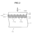
- Figure 1 is a schematic perspective view showing an optical recording medium that is a preferred embodiment of the present invention and Figure 2 is a schematic enlarged cross-sectional view indicated by A in Figure 1.
- the an optical recording medium 10 is constituted as a write-once type optical recording medium and as shown in Figure 2, it includes a support substrate 11, a reflective layer 12 formed on the surface of the support substrate 11, a second dielectric layer 13 formed on the surface of the reflective layer 12, a recording layer 14 formed on the surface of the second dielectric layer 13, a first dielectric layer 15 formed on the surface of the recording layer 14 and a light transmission layer 16 formed on the surface of the first dielectric layer 15.
- the recording layer 14 is constituted by a second recording film 22 formed on the surface of the second dielectric layer 13 and a first recording film 21 formed on the surface of the second recording layer 22.
- a laser beam L is projected onto a light incident surface 16a of the light transmission layer 16, thereby recording data in the optical recording medium 10 or reproducing data from the optical recording medium 10.
- the support substrate 11 serves as a support for ensuring mechanical strength required for the optical recording medium 10.
- the material used to form the support substrate 11 is not particularly limited insofar as the support substrate 11 can serve as the support of the optical recording medium 10.
- the support substrate 11 can be formed of glass, ceramic, resin or the like.
- resin is preferably used for forming the support substrate 11 since resin can be easily shaped.
- Illustrative examples of resins suitable for forming the support substrate 11 include polycarbonate resin, polyolefin resin, acrylic resin, epoxy resin, polystyrene resin, polyethylene resin, polypropylene resin, silicone resin, fluoropolymers, acrylonitrile butadiene styrene resin, urethane resin and the like.
- polycarbonate resin and polyolefin resin are most preferably used for forming the support substrate 11 from the viewpoint of easy processing, optical characteristics and the like.
- the support substrate 11 has a thickness of about 1.2 mm.
- the shape of the support substrate 11 is not particularly limited but is normally disk-like, card-like or sheet-like.
- grooves 11a and lands 11b are alternately formed on the surface of the support substrate 11.
- the grooves 11a and/or lands 11b serve as a guide track for the laser beam L when data are recorded or when data are reproduced.
- the reflective layer 12 serves to reflect the laser beam L entering through the light transmission layer 16 so as to emit it from the light transmission layer 16.
- the thickness of the reflective layer 12 is not particularly limited but is preferably from 5 nm to 300 nm, more preferably from 20 nm to 200 nm.
- the material used to form the reflective layer 12 is not particularly limited insofar as it can reflect a laser beam L, and the reflective layer 12 can be formed of Mg, Al, Ti, Cr, Fe, Co, Ni, Cu, Zn, Ge, Ag, Pt, Au and the like. Among these materials, it is preferable to form the reflective layer 12 of a metal material having a high reflection characteristic, such as Al, Au, Ag, Cu or alloy containing at least one of these metals, such as alloy of Al and Ti.
- a metal material having a high reflection characteristic such as Al, Au, Ag, Cu or alloy containing at least one of these metals, such as alloy of Al and Ti.
- the reflective layer 12 is provided in order to increase the difference in reflection coefficient between a recorded region and an unrecorded region by a multiple interference effect when the laser beam L is used to reproduce data recorded in the recording layer 14, thereby obtaining a higher reproduced signal (C/N ratio).
- the first dielectric layer 15 and the second dielectric layer 13 serve to protect the recording layer 14 constituted by the first recording film 21 and the second recording film 22. Degradation of data recorded in the recording layer 14 can be prevented over a long period by the first dielectric layer 15 and the second dielectric layer 13.
- Each of the first dielectric layer 15 and the second dielectric layer 13 contains Ta 2 O 5 or TiO 2 and is added with nitrogen.
- the refractive index n and the extinction coefficient k of Ta 2 O 5 or TiO 2 greatly depend on the wavelength of the incident light, in the case where the dielectric layer is formed of Ta 2 O 5 or TiO 2 , the refractive index n of the dielectric layer becomes low or the extinction coefficient k of the dielectric layer becomes high depending upon the wavelength of the laser beam used for recording and reproducing data, thereby degrading optical characteristics of the optical recording medium and, in particular, if a dielectric layer is formed of an oxide in a next-generation type optical recording medium in which data are recorded and reproduced using a laser beam in the blue wavelength band, it will be impossible to obtain excellent optical characteristics.
- the difference ( n0 - n ) between the refractive index n0 of a dielectric layer containing Ta 2 O 5 or TiO 2 as a primary component and no nitrogen as an additive and the refractive index n of a dielectric layer containing Ta 2 O 5 or TiO 2 as a primary component and nitrogen as an additive becomes smaller as the wavelength of a laser beam L used for recording and reproducing data is shorter and the difference ( k0- k ) between the extinction coefficient k0 of a dielectric layer containing Ta 2 O 5 or TiO 2 as a primary component and no nitrogen as an additive and the extinction coefficient k of a dielectric layer containing Ta 2 O 5 or TiO 2 as a primary component and nitrogen as an additive becomes larger as the wavelength of a laser beam L used for recording and reproducing data is shorter.
- a further study carried out by the inventors of the present invention revealed that the refractive index n0 of a dielectric layer containing Ta 2 O 5 as a primary component but no nitrogen as an additive greatly decreases as the wavelength of the laser beam L becomes shorter, while the refractive index n of a dielectric layer containing Ta 2 O 5 as a primary component and a prescribed amount of nitrogen as an additive greatly increases as the wavelength of the laser beam L becomes shorter, and that the extinction coefficient k of a dielectric layer containing Ta 2 O 5 as a primary component and a prescribed amount of nitrogen as an additive is smaller than the extinction coefficient k0 of a dielectric layer containing Ta 2 O 5 as a primary component but no nitrogen as an additive and becomes smaller as the wavelength of the laser beam L becomes shorter.
- the refractive index n0 of a dielectric layer containing TiO 2 as a primary component but no nitrogen as an additive stays almost constant even if the wavelength of the laser beam L becomes shorter, while the refractive index n of a dielectric layer containing TiO 2 as a primary component and a predetermined amount of nitrogen as an additive increases as the wavelength of the laser beam L becomes shorter, and that the extinction coefficient k of a dielectric layer containing TiO 2 as a primary component and a prescribed amount of nitrogen as an additive is smaller than the extinction coefficient k0 of a dielectric layer containing TiO 2 as a primary component but no nitrogen as an additive and becomes smaller as the wavelength of the laser beam L becomes shorter.
- the amounts of nitrogen added to the first dielectric layer 15 and the second dielectric layer 13 are determined so that the refractive indexes n of the first dielectric layer 15 and the second dielectric layer 13 are sufficiently high and the extinction coefficients k thereof are sufficiently low when a laser beam L having a wavelength of 405 nm is used for recording and reproducing data.
- the first dielectric layer 15 and the second dielectric layer 13 may be formed of the same material or of different materials.
- the thickness of the first dielectric layer 15 and the second dielectric layer 13 is not particularly limited but is preferably from 3 nm to 200 nm. If the first dielectric layer 15 or the second dielectric layer 13 is thinner than 3 nm, it is difficult to obtain the above-described advantages. On the other hand, if the first dielectric layer 15 or the second dielectric layer 13 is thicker than 200 nm, it takes a long time to form the first dielectric layers 15 and the second dielectric layers 13, thereby lowering the productivity of the optical recording medium 10, and cracks may be generated in the optical recording medium 10 owing to stress present in the first dielectric layers 15 and/or the second dielectric layer 13.
- the recording layer 14 is adapted for recording data therein.
- the recording layer 14 is constituted by the first recording film 21 and the second recording film 22 and the first recording film 21 is disposed on the side of the light transmission layer 16 and the second recording film 22 is disposed on the side of the support substrate 11.
- the first recording film 21 contains an element selected from the group consisting of Si, Ge and Sn as a primary component and the second recording film 22 contains Cu as a primary component.
- Cu contained in the second recording film 22 as a primary component quickly mixes with the element contained in the first recording film 21 to form a record mark when irradiated with a laser beam L, thereby enabling data to be quickly recorded in the first recording film 21 and the second recording film 22.
- one or more elements selected from a group consisting of Mg, Al, Cu, Ag and Au may be further added to the first recording film 21.
- At least one element selected from the group consisting of Al, Si, Zn, Mg and Au may be further added to the second recording film 22.
- the amount of the element (elements) added to the second recording film 22 is preferably equal to or more than 1 atomic % and less than 50 atomic %.
- the surface smoothness of the first recording layer 31 irradiated with the laser beam L becomes worse as the total thickness of the first recording film 21 and the second recording film 22 becomes thicker. As a result, the noise level of the reproduced signal becomes higher and the recording sensitivity is lowered. On the other hand, in the case where the total thickness of the first recording film 21 and the second recording film 22 is too small, the change in reflection coefficient between before and after irradiation with the laser beam L is small, so that a reproduced signal having high strength (C/N ratio) cannot be obtained. Moreover, it becomes difficult to control the thickness of the first recording film 21 and the second recording film 22.
- the first recording film 21 and the second recording film 22 are formed so that the total thickness thereof is from 2 nm to 40 nm.
- the total thickness of the first recording film 21 and the second recording film 22 is preferably from 2 nm to 20 nm and more preferably 2 nm to 15 nm.
- the individual thicknesses of the first recording film 21 and the second recording film 22 are not particularly limited but in order to considerably improve the recording sensitivity and greatly increase the change in reflection coefficient between before and after irradiation with the laser beam L, the thickness of the first recording film 21 is preferably from 1 nm to 30 nm and the thickness of the second recording film 22 is preferably from 1 nm to 30 nm. Further, it is preferable to define the ratio of the thickness of the first recording film 21 to the thickness of the second recording film 22 (thickness of first recording film 21 / thickness of second recording film 22) to be from 0.2 to 5.0.
- the light transmission layer 16 serves to transmit a laser beam L and preferably has a thickness of 10 ⁇ m to 300 ⁇ m. More preferably, the light transmission layer 16 has a thickness of 50 ⁇ m to 150 ⁇ m.
- the material used to form the light transmission layer 16 is not particularly limited but in the case where the light transmission layer 16 is to be formed by the spin coating process or the like, ultraviolet ray curable resin, electron beam curable resin or the like is preferably used. More preferably, the light transmission layer 16 is formed of ultraviolet ray curable resin.
- the light transmission layer 16 may be formed by adhering a sheet made of light transmittable resin to the surface of the first dielectric layer 15 using an adhesive agent.
- the optical recording medium 10 having the above-described configuration can, for example, be fabricated in the following manner.
- the support substrate 11 having the groove 11a and the land 11d on the surface thereof is first fabricated by injection molding using a stamper (not shown).
- the reflective layer 12 is further formed on the surface of the support substrate 11.
- the reflective layer 12 can be formed by a gas phase growth process using chemical species containing elements for forming the reflective layer 12.
- gas phase growth processes include vacuum deposition process, sputtering process and the like.
- the second dielectric layer 13 is then formed on surface of the reflective layer 12.
- the second dielectric layer 13 is formed by a sputtering process using a mixed gas of argon gas and nitrogen gas as sputtering gas and an oxide such as Ta 2 O 5 , TiO 2 or the like as a target.
- the second dielectric layer 13 contains an oxide such as Ta 2 O 5 , or TiO 2 as a primary component and is added with nitrogen.
- the nitrogen content of the second dielectric layer 13 is determined so that the second dielectric layer 13 has a high refractive index n and a low extinction coefficient k and the nitrogen content of the second dielectric layer 13 can be controlled by controlling the amount of nitrogen gas in the sputtering gas.
- the second recording film 22 is further formed on the second dielectric layer 13.
- the second recording layer 22 can be also formed by a gas phase growth process using chemical species containing elements for forming the second recording film 22.
- the first recording film 21 is then formed on the second recording film 22.
- the first recording film 21 can be also formed by a gas phase growth process using chemical species containing elements for forming the first recording film 21.
- the first recording film 21 and the second recording film 22 are formed so that the total thickness thereof is from 2 nm to 40 nm, it is possible to improve the surface smoothness of the first recording film 21.
- the first dielectric layer 15 is further formed on the first recording film 31.
- the first dielectric layer 15 is formed by a sputtering process using a mixed gas of argon gas and nitrogen gas as sputtering gas and an oxide such as Ta 2 O 5 , TiO 2 or the like as a target.
- the first dielectric layer 15 contains an oxide such as Ta 2 O 5 , or TiO 2 as a primary component and is added with nitrogen.
- the nitrogen content of the first dielectric layer 15 is determined so that the first dielectric layer 15 has a high refractive index n and a low extinction coefficient k and the nitrogen content of the first dielectric layer 15 can be controlled by controlling the amount of nitrogen gas in the sputtering gas.
- the light transmission layer 16 is formed on the first dielectric layer 15.
- the light transmission layer 16 can be formed, for example, by applying an acrylic ultraviolet ray curable resin or epoxy ultraviolet ray curable resin adjusted to an appropriate viscosity onto the surface of the second dielectric layer 15 by spin coating to form a coating layer and irradiating the coating layer with ultraviolet rays to cure the coating layer.
- the optical recording medium 10 was fabricated.
- Data are recorded in the optical recording medium 10 of the above-described configuration, in the following manner, for example.
- the first recording film 21 and the second recording film 22 are first irradiated via the light transmission layer 16 with a laser beam L having predetermined power.
- a laser beam L having a wavelength ⁇ of 405 nm is projected onto the optical recording medium 10 via an objective lens having a numerical aperture NA of 0.85.
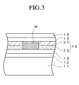
- an element contained in the first recording film 21 as a primary component and an element contained in the second recording film 22 as a primary component are mixed at a region irradiated with the laser beam L and as shown in Figure 3, a mixed region composed of a mixture of the primary component element of the first recording film 21 and the primary component element of the second recording film 22 is produced and a record mark M is formed.
- the reflection coefficient of the region in which the record mark M is formed markedly changes. Since the reflection coefficient of the thus formed record mark M is therefore greatly different from that of the region surrounding the mixed region M, it is possible to obtain a high reproduced signal (C/N ratio) when optically recorded information is reproduced.
- the amounts of nitrogen added to the first dielectric layer 15 and the second dielectric layer 13 are determined so that the refractive indexes n of the first dielectric layer 15 and the second dielectric layer 13 are sufficiently high and the extinction coefficients k thereof are sufficiently low with respect to the laser beam L having a wavelength of 405 nm, when data are recorded in the optical recording medium 10, it is possible to decrease the energy of the laser beam L absorbed in the first dielectric layer 15 and the second dielectric layer 13 and improve the recording sensitivity of the optical recording medium 10.
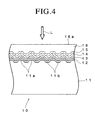
- Figure 4 is a schematic cross sectional view showing a layer configuration of an optical recording medium which is another preferred embodiment of the present invention.
- the optical recording medium 10 is constituted as a data rewritable type optical recording medium and as shown in Figure 4, it includes a support substrate 11, a reflective layer 12 formed on the surface of the support substrate 11, a second dielectric layer 13 formed on the surface of the reflective layer 12, a recording layer 14 formed on the surface of the second dielectric layer 13, a first dielectric layer 15 formed on the surface of the recording layer 14 and a light transmission layer 16 formed on the surface of the first dielectric layer 15.
- a laser beam L is also projected onto a light incident surface 16a of the light transmission layer 16, thereby recording data in the optical recording medium 10 or reproducing data from the optical recording medium 10.
- Each of the support substrate 11, the reflective layer 12 and the light transmission layer 16 of the optical recording medium 10 according to this embodiment serves and is constituted similarly to the corresponding one of the support substrate 11, the reflective layer 12 and the light transmission layer 16 of the optical recording medium 10 according to the previous embodiment shown in Figure 2.
- Each of the first dielectric layer 15 and the second dielectric layer 13 is constituted similarly to that of the optical recording medium 10 according to the previous embodiment shown in Figure 2 and differ therefrom only in that they serve to protect the recording layer 14.
- the amounts of nitrogen to be added to the first dielectric layer 15 and the second dielectric layer 13 are also determined so that the refractive indexes n of the first dielectric layer 15 and the second dielectric layer 13 are sufficiently high and the extinction coefficients k thereof are sufficiently low when a laser beam L having a wavelength of 405 nm is used for recording and reproducing data.
- the recording layer 14 is adapted for recording data therein.
- the recording layer 14 is formed of a phase change material. Utilizing the difference in the reflection coefficients between the case where the recording layer 14 is in a crystal phase and the case where it is in an amorphous phase, data are recorded in the recording layer 14 and data are reproduced from the recording layer 14.
- the material for forming the recording layer 14 is not particularly limited but a material capable of changing from an amorphous phase to a crystal phase in a short time is preferable in order to enable direct overwriting of data at a high velocity.
- a material capable of changing from an amorphous phase to a crystal phase in a short time is preferable in order to enable direct overwriting of data at a high velocity.
- materials having such a characteristic include a SbTe system material.
- SbTe may be used alone or a SbTe system material to which additives are added in order to shorten time required for crystallization and improve the long-term storage reliability of the optical recording medium 10 may be used.
- the element M is not particularly limited, it is preferable for the element M to be one or more elements selected from the group consisting of In, Ag, Au, Bi, Se, Al, P, Ge, H, Si, C, V, W, Ta, Zn, Mn, Ti, Sn, Pd, N, O and rare earth elements in order to shorten time required for crystallization and improve the storage reliability of the optical recording medium 10. It is particularly preferable for the element M to be one or more elements selected from the group consisting of Ag, In, Ge and rare earth elements for improving the storage reliability of the optical recording medium 10.
- the optical recording medium 10 having the above-described configuration can, for example, be fabricated in the following manner.
- the support substrate 11 is first fabricated and the reflective layer 12 is formed on the surface of the support substrate 11.
- the second dielectric layer 13 is then formed on surface of the reflective layer 12.
- the recording layer 14 is further formed on the second dielectric layer 13.
- the recording layer 14 can be also formed by a gas phase growth process using chemical species containing elements for forming the recording layer 14.
- the first dielectric layer 15 is then formed on the recording layer 14.
- the light transmission layer 16 is formed on the first dielectric layer 15.
- the light transmission layer 16 can be formed, for example, by applying an acrylic ultraviolet ray curable resin or epoxy ultraviolet ray curable resin adjusted to an appropriate viscosity onto the surface of the second dielectric layer 15 by spin coating to form a coating layer and irradiating the coating layer with ultraviolet rays to cure the coating layer.
- optical recording medium 10 shown in Figure 4 was fabricated.
- Data are recorded in the optical recording medium 10 of the above-described configuration, in the following manner, for example.
- the first layer 14 is first irradiated via the light transmission layer 16 with a laser beam L having predetermined power.
- a laser beam L having a wavelength ⁇ of 405 nm is projected onto the optical recording medium 10 via an objective lens having a numerical aperture NA of 0.85.
- a record mark is formed by the region in the amorphous state of the recording layer 14.
- the length of the record mark and the length of the blank region between the record mark and the neighboring record mark in the direction of the track constitute data recorded in the recording layer 14.
- the amounts of nitrogen added to the first dielectric layer 15 and the second dielectric layer 13 are determined so that the refractive indexes n of the first dielectric layer 15 and the second dielectric layer 13 are sufficiently high and the extinction coefficients k thereof are sufficiently low with respect to the laser beam L having a wavelength of 405 nm, it is possible to decrease the energy of the laser beam L absorbed in the first dielectric layer 15 and the second dielectric layer 13 and improve the recording sensitivity of the optical recording medium 10.
- the light incident plane 16a of the light transmission layer 16 is irradiated with a laser beam L whose intensity is modulated and the focus of the laser beam L is adjusted onto the recording layer 14.
- the reflection coefficients of the recording layer 14 are different between a region in an amorphous state and a region in a crystallized state, it is possible to reproduce data recorded in the recording layer 14 by detecting the amount of the laser beam L reflected from the recording layer 14.
- the amounts of nitrogen added to the first dielectric layer 15 and the second dielectric layer 13 are determined so that the refractive indexes n of the first dielectric layer 15 and the second dielectric layer 13 are sufficiently high and the extinction coefficients k thereof are sufficiently low with respect to the laser beam L having a wavelength of 405 nm, it is possible to increase modulation, namely, the difference in reflection coefficients between a region of the recording layer where a record mark is formed and a region thereof where no record mark is formed and prevent the reflective coefficient of the recording layer 14 from decreasing.
- the amounts of nitrogen added to the first dielectric layer 15 and the second dielectric layer 13 are determined so that the refractive indexes n of the first dielectric layer 15 and the second dielectric layer 13 are sufficiently high and the extinction coefficients k thereof are sufficiently low with respect to the laser beam L having a wavelength of 405 nm, when data are recorded in the optical recording medium 10, it is possible to decrease the energy of the laser beam L absorbed in the first dielectric layer 15 and the second dielectric layer 13 and improve the recording sensitivity of the optical recording medium 10.
- Figure 5 is a cross-sectional view showing a layer configuration of an optical recording medium which is a further embodiment of the present invention.
- An optical recording medium 30 is constituted as a write once type optical recording medium and as shown in Figure 5, it includes a support substrate 31, a transparent intermediate layer 32, a light transmission layer 33, an L0 layer 40 formed the support substrate 31 and the transparent intermediate layer 32 and an L1 layer 50 formed between the transparent layer 32 and the light transmission layer 33.
- the L0 layer 40 and the L1 layer 50 are recording layers in which data are recorded, i.e., the optical recording medium 30 according to this embodiment includes two recording layers.
- the L0 layer 40 constitutes a recording layer far from the light incident plane 33a and is constituted by laminating a reflective film 41, a fourth dielectric film 42, a second L0 recording film 43a, a first L0 recording film 43b and a third dielectric film 44 from the side of the support substrate 31.
- the L1 layer 50 constitutes a recording layer close to a light incident plane 33a and is constituted by laminating a reflective film 51, a second dielectric film 52, a second L1 recording film 53a, a first L1 recording film 53b and a first dielectric film 53b from the side of the support substrate 31.
- a laser beam L is projected thereon through the L1 layer 50 located closer to the light transmission layer 33.
- the support substrate 31 serves as a support for ensuring mechanical strength required for the optical recording medium 30 and is constituted similarly to the support substrate 11 of the optical recording medium 10 shown in Figure 2.
- the transparent intermediate layer 32 serves to space the L0 layer 40 and the L1 layer 50 apart by a physically and optically sufficient distance.
- grooves 32a and lands 32b are alternately formed on the surface of the transparent intermediate layer 32 so as to correspond to grooves 31a and lands 31b formed on the support substrate 31.
- the grooves 32a and/or lands 32b formed on the surface of the transparent intermediate layer 32 serve as a guide track for the laser beam L when data are recorded in the L0 layer 40 or when data are reproduced from the L0 layer 40.
- the transparent intermediate layer 32 it is preferable to form the transparent intermediate layer 32 so as to have a thickness of 10 ⁇ m to 50 ⁇ m and it is more preferable to form it so as to have a thickness of 15 ⁇ m to 40 ⁇ m.
- the transparent intermediate layer 32 It is necessary for the transparent intermediate layer 32 to have sufficiently high light transmittance since the laser beam L passes through the transparent intermediate layer 32 when data are recorded in the L0 layer 40 and data recorded in the L0 layer 40 are reproduced.
- the material for forming the transparent intermediate layer 32 is not particularly limited and an ultraviolet ray curable acrylic resin is preferably used for forming the transparent intermediate layer 32.
- the light transmission layer 33 serves to transmit the laser beam L and the light incident plane 33a is constituted by one of the surfaces thereof.
- the light transmission layer 33 is constituted similarly to the light transmission layer 16 of the optical recording medium 10 shown in Figure 2.
- the L0 layer 40 includes a first L0 recording film 43b containing an element selected from a group consisting of Si, Ge and Sn as a primary component and a second L0 recording film 43a containing Cu as a primary component.
- the optical recording medium 30 In order to lower the noise level of a reproduced signal and improve the storage reliability of the optical recording medium 30, it is preferable to add one or more elements selected from the group consisting of Al, Zn, Sn, Mg and Au to the second L0 recording film 43a.
- the L1 layer 50 includes a first L1 recording film 53b containing Si as a primary component and a second L1 recording film 53a containing Cu as a primary component.
- the optical recording medium 30 In order to lower the noise level of a reproduced signal and improve the storage reliability of the optical recording medium 30, it is preferable to add one or more elements selected from the group consisting of Al, Zn, Sn, Mg and Au to the second L1 recording film 53a.
- each of the fourth dielectric film 42 and the third dielectric film 44 included in the L0 layer 40 and the second dielectric film 52 and the first dielectric film 54 contains Ta 2 O 5 or TiO 2 as a primary component and nitrogen as an additive and the amount of nitrogen added to each of the first dielectric film 54, the second dielectric film 52, the third dielectric film 44 and the fourth dielectric film 42 is determined so that the refractive index n thereof is sufficiently high and the extinction coefficient k thereof is sufficiently low with respect to a laser beam L having a wavelength of 405 nm.
- Figure 6 is a schematic enlarged cross-sectional view showing the optical recording medium 30 shown in Figure 5 after the L1 layer 50 was irradiated with a laser beam L.
- the reflection coefficient of the region of the L0 layer 40 or the L1 layer 50 where the record mark M is formed in this manner is greatly different from that of a region of the L0 layer 40 or the L1 layer 50 surrounding the region where the record mark M is formed, it is possible to obtain a high reproduced signal (C/N ratio) by projecting the laser beam L onto the L0 layer 40 or the L1 layer 50 and detecting the amount of the laser beam L reflected by the L0 layer 40 or the L1 layer 50.
- the amounts of nitrogen added to the fourth dielectric film 42 and the third dielectric film 44 included in the L0 layer 40 are determined so that the refractive indexes n of the fourth dielectric film 42 and the third dielectric film 44 are sufficiently high and the extinction coefficients k thereof are sufficiently low with respect to the laser beam L having a wavelength of 405 nm, when data are recorded in the L0 layer 40 of the optical recording medium 10, it is possible to decrease the energy of the laser beam L absorbed in the fourth dielectric film 42 and the third dielectric film 44 and improve the recording sensitivity of the L0 layer 40 of the optical recording medium 10.
- the amounts of nitrogen added to the second dielectric film 52 and the first dielectric film 54 included in the L1 layer 50 are determined so that the refractive indexes n of the second dielectric film 52 and the first dielectric film 54 are sufficiently high and the extinction coefficients k thereof are sufficiently low with respect to the laser beam L having a wavelength of 405 nm, when data are recorded in the L1 layer 50 of the optical recording medium 10, it is possible to decrease the energy of the laser beam L absorbed in the second dielectric film 52 and the first dielectric film 54 and improve the recording sensitivity of the L1 layer 50 of the optical recording medium 10.
- the amounts of nitrogen added to the second dielectric film 52 and the first dielectric film 54 included in the L1 layer 50 are determined so that the refractive indexes n of the second dielectric film 52 and the first dielectric film 54 are sufficiently high and the extinction coefficients k thereof are sufficiently low with respect to the laser beam L having a wavelength of 405 nm, the light transmittance of the L1 layer 50 can be increased and it is therefore possible to markedly improve the data recording characteristic in the L0 layer 40 and the data reproducing characteristic from the L0 layer 40.
- a disk-like polycarbonate substrate having a thickness of 1.1 mm and a diameter of 120 mm was first fabricated using an injection molding process.
- the thus fabricated polycarbonate substrate was then set on a sputtering apparatus and a sputtering process was performed at a power of 800 W using a Ta 2 O 5 target, thereby forming a dielectric layer having a thickness of 30 nm and containing Ta 2 O 5 as a primary component on the surface of the polycarbonate substrate.
- a mixed gas of argon gas and nitrogen gas was employed as a sputtering gas and samples #1-1 to #1-6 were fabricated to give their dielectric layers different nitrogen contents from each other by varying the flow rate of nitrogen from 0 to 35 SCCM.
- the amount of nitrogen contained in the dielectric layer of each of the samples #1-1 to #1-6 was measured and the relationship between the composition of the mixed gas used as the sputtering gas and the amounts of nitrogen added to the dielectric layers of the samples #1-1 to #1-6 was determined.
- the amount of nitrogen added to each of the dielectric layer was obtained by multiplying the peak areas of the 4f peak of tantalum (peak position: about 28.2 to 37.4 eV), the 1s peak of oxygen (peak position: about 523 to 543 eV) and the 1s peak of nitrogen (peak position: about 390 to 410 eV) measured by the ESCA (Electron Spectroscopy for Chemical Analysis), namely, XPS (X-ray photoelectron spectroscopy) by the corresponding sensitivity factors of the peaks, namely, 0.596 of that of the 4f peak of tantalum, 2.994 of that of the 1s peak of oxygen and 4.505 of that of the 1s peak of nitrogen.
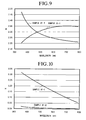
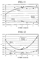
- a laser beam having a wavelength of 405 nm and a laser beam having a wavelength of 680 nm were projected onto each of the samples #1-1 to #1-6, whereby the refractive index n and the extinction coefficient k thereof were measured and the relationship between the amount (atomic %) of nitrogen added to the dielectric layers and the refractive index n of the dielectric layer and the relationship between the amount (atomic %) of nitrogen added to the dielectric layers and the extinction coefficient k of the dielectric layer were obtained.
- both the extinction coefficient k of the dielectric layer with respect to the laser beam having a wavelength of 405 nm and the extinction coefficient k of the dielectric layer with respect to the laser beam having a wavelength of 680 nm were equal to zero when about 6 atomic % to about 10 atomic % of nitrogen was added to the dielectric layer but increased in accordance with increase in the amount of nitrogen added to the dielectric layer when it exceeded about 10 atomic %.
- a laser beam was projected onto the samples #1-1 and #1-2 and the refractive index n and the extinction coefficient k of each dielectric layer were measured while varying the wavelength of the laser beam in the range between 350 nm and 800 nm, whereby the relationship between the wavelength of the laser beam and the refractive index n of the dielectric layers and the relationship between the wavelength of the laser beam and the extinction coefficient k of the dielectric layers were obtained.
- the extinction coefficient k of the sample #1-1 including the dielectric layer containing Ta 2 O 5 as a primary component but no nitrogen as an additive increased substantially linearly as the wavelength of the laser beam became shorter
- the extinction coefficient k of the sample #1-2 including the dielectric layer containing Ta 2 O 5 as a primary component and 3.3 atomic % of nitrogen as an additive was substantially constant even if the wavelength of the laser beam varied and that the extinction coefficient k of the sample #1-1 was higher than that of the sample #1-2 with respect to the laser beam having a wavelength of from 350 nm to 800 nm and the difference therebetween became larger as the wavelength of the laser beam became shorter.
- a disk-like polycarbonate substrate having a thickness of 1.1 mm and a diameter of 120 mm was first fabricated using an injection molding process.
- the thus fabricated polycarbonate substrate was then set on a sputtering apparatus and a sputtering process was performed at a power of 800 W using a TiO 2 target, thereby forming a dielectric layer having a thickness of 30 nm and containing TiO 2 as a primary component on the surface of the polycarbonate substrate.
- a mixed gas of argon gas and nitrogen gas was employed as a sputtering gas and samples #2-1 to #2-8 were fabricated to give their dielectric layers different nitrogen contents from each other by varying the flow rate of nitrogen from 0 to 35 SCCM.
- the amount of nitrogen contained in the dielectric layer of each of the sample #2-1 to the sample #2-6 was measured and the relationship between the composition of the mixed gas used as the sputtering gas and the amounts of nitrogen added to the dielectric layers of the sample #2-1 to the sample #2-6 was determined.
- the amount of nitrogen added to each of the dielectric layers was obtained by multiplying the peak areas of the 2p peak of titanium (peak position: about 443.8 to 473.8 eV), the 1s peak of oxygen (peak position: about 523 to 543 eV) and the 1s peak of nitrogen (peak position: about 390 to 410 eV) measured by ESCA (Electron Spectroscopy for Chemical Analysis), namely, XPS (X-ray photoelectron spectroscopy) by the corresponding sensitivity factors of the peaks, namely, 1.703 of that of the 2p peak of titanium, 2.994 of that of the 1s peak of oxygen and 4.505 of that of the 1s peak of nitrogen.
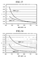
- a laser beam having a wavelength of 405 nm and a laser beam having a wavelength of 680 nm were projected onto each of the samples #2-1 to #2-8, whereby the refractive index n and the extinction coefficient k thereof were measured and the relationship between the amount (atomic %) of nitrogen added to the dielectric layers and the refractive index n of the dielectric layer and the relationship between the amount (atomic %) of nitrogen added to the dielectric layers and the extinction coefficient k of the dielectric layers were obtained.
- the extinction coefficient k of the dielectric layer with respect to the laser beam having a wavelength of 680 nm decreased as the amount of nitrogen added to the dielectric layer was increased but that when the amount of nitrogen exceeded about 3 atomic %, the extinction coefficient k thereof increased.
- a laser beam was projected onto the samples #2-1 and #2-3 and the refractive index n and the extinction coefficient k of the dielectric layers were measured while varying the wavelength of the laser beam in the range between 350 nm and 800 nm, whereby the relationship between the wavelength of the laser beam and the refractive index n of the dielectric layer and the relationship between the wavelength of the laser beam and the extinction coefficient k of the dielectric layer were determined.
- An optical recording medium sample #3-1 was fabricated in the following manner.
- a disk-like polycarbonate substrate having a thickness of 1.1 mm and a diameter of 120 mm was first fabricated using an injection molding process.
- the polycarbonate substrate was set on a sputtering apparatus and a reflective film containing Ag as a primary component and having a thickness of 100 nm, a second dielectric film containing TiO 2 as a primary component and 2.9 atomic % of nitrogen as an additive and having a thickness of 17 nm, a second recording film containing Cu as a primary component and 23 atomic % of Al and 13 atomic % of Au as additives and having a thickness of 5 nm, a first recording film containing Si as a primary component and having a thickness of 5 nm, a first dielectric film containing TiO 2 as a primary component and 2.9 atomic % of nitrogen as an additive and having a thickness of 17 nm were sequentially formed on the thus fabricated polycarbonate substrate using the sputtering process.
- the first dielectric film was coated using the spin coating method with a resin solution prepared by dissolving acrylic ultraviolet curing resin in a solvent to form a coating layer and the coating layer was irradiated with ultraviolet rays, thereby curing the acrylic ultraviolet curing resin to form a protective layer having a thickness of 100 ⁇ m.
- optical recording medium sample #3-2 was fabricated in the following manner.
- a disk-like polycarbonate substrate having a thickness of 1.1 mm and a diameter of 120 mm was first fabricated using an injection molding process.
- the polycarbonate substrate was set on the sputtering apparatus and a reflective film containing Ag as a primary component and having a thickness of 100 nm, a second dielectric film containing TiO 2 as a primary component and having a thickness of 20nm, a second recording film containing Cu as a primary component and 23 atomic % of Al and 13 atomic % of Au as additives and having a thickness of 5 nm, a first recording film containing Si as a primary component and having a thickness of 5 nm, a first dielectric film containing TiO 2 as a primary component and 2.9 atomic % of nitrogen as an additive and having a thickness of 23 nm were sequentially formed on the thus fabricated polycarbonate substrate using the sputtering process.
- the first dielectric film was coated using the spin coating method with a resin solution prepared by dissolving acrylic ultraviolet curing resin in a solvent to form a coating layer and the coating layer was irradiated with ultraviolet rays, thereby curing the acrylic ultraviolet curing resin to form a protective layer having a thickness of 100 ⁇ m.
- the modulation and the recording sensitivity of an optical recording medium can be improved by adding nitrogen to a first dielectric layer and a second dielectric layer.
- each of the first dielectric layer 15 and the second dielectric layer 13 contains nitrogen as an additive in the embodiment shown in Figures 2 and 3 and the embodiment shown in Figure 4 and each of the fourth dielectric film 42 and the third dielectric film 44 included in the L0 layer 40 and the second dielectric film 52 and the first dielectric film 54 contains nitrogen as an additive.
- At least a dielectric layer or a dielectric film on the side of a light incidence plane with respect to a recording layer prefferably contains nitrogen as an additive and it is preferable for a dielectric layer or a dielectric film on the side of the light incidence plane with respect to an associated recording layer to contain nitrogen as an additive.
- first recording film 21 and the second recording film 22 are formed in contact with each other, it is not absolutely necessary to form the first recording film 21 and the second recording film 22 in contact with each other but it is sufficient for the second recording film 22 to be so located in the vicinity of the first recording film 21 as to enable formation of a mixed region including the primary component element of the first recording film 21 and the primary component element of the second recording film 22 when the region is irradiated with a laser beam. Further, one or more other layers such as a dielectric layer may be interposed between the first recording film 21 and the second recording film 22.
- each of the optical recording media 10 in the embodiment shown in Figure 2 and 3 and in the embodiment shown in Figure 4 includes the reflective layer 12, and the L0 layer 40 and the L1 layer 50 respectively include the reflective film 41 and the reflective film 51.
- the reflective layer 12, the reflective film 41 and the reflective film 51 may be omitted.
- an optical recording medium which can exhibit excellent optical characteristics with respect to a laser beam of desired wavelength used for recording data and reproducing data and a method for manufacturing the same.
- an optical recording medium which can exhibit excellent optical characteristics with respect to a laser beam in the blue wavelength band and used for recording data and reproducing data and a method for manufacturing the same.
Landscapes
- Engineering & Computer Science (AREA)
- Manufacturing & Machinery (AREA)
- Chemical & Material Sciences (AREA)
- Inorganic Chemistry (AREA)
- Optical Record Carriers And Manufacture Thereof (AREA)
- Thermal Transfer Or Thermal Recording In General (AREA)
Applications Claiming Priority (4)
| Application Number | Priority Date | Filing Date | Title |
|---|---|---|---|
| JP2002307369 | 2002-10-22 | ||
| JP2002307369 | 2002-10-22 | ||
| JP2003005635 | 2003-01-14 | ||
| JP2003005635 | 2003-01-14 |
Publications (1)
| Publication Number | Publication Date |
|---|---|
| EP1414029A2 true EP1414029A2 (fr) | 2004-04-28 |
Family
ID=32072527
Family Applications (1)
| Application Number | Title | Priority Date | Filing Date |
|---|---|---|---|
| EP20030023871 Withdrawn EP1414029A2 (fr) | 2002-10-22 | 2003-10-21 | Support d'enregistrement optique et son procédé de fabrication |
Country Status (4)
| Country | Link |
|---|---|
| US (1) | US20040076907A1 (fr) |
| EP (1) | EP1414029A2 (fr) |
| KR (1) | KR20040035564A (fr) |
| TW (1) | TWI273594B (fr) |
Families Citing this family (21)
| Publication number | Priority date | Publication date | Assignee | Title |
|---|---|---|---|---|
| TWI254301B (en) * | 2002-04-05 | 2006-05-01 | Tdk Corp | Optical recording medium and method for optically recording information in the same |
| TWI254934B (en) * | 2002-04-26 | 2006-05-11 | Tdk Corp | Optical recording medium and method for optically recording data in the same |
| US20040038080A1 (en) * | 2002-07-01 | 2004-02-26 | Tdk Corporation | Optical recording medium and method for recording data in the same |
| JP4092147B2 (ja) * | 2002-07-04 | 2008-05-28 | Tdk株式会社 | 光記録媒体及び光記録方法 |
| JP4282285B2 (ja) * | 2002-08-12 | 2009-06-17 | Tdk株式会社 | 光記録媒体及び光記録方法 |
| US7781146B2 (en) * | 2002-11-22 | 2010-08-24 | Tdk Corporation | Optical recording medium |
| US7932015B2 (en) | 2003-01-08 | 2011-04-26 | Tdk Corporation | Optical recording medium |
| JP2004355743A (ja) * | 2003-05-30 | 2004-12-16 | Tdk Corp | 光情報記録媒体 |
| EP1647013B1 (fr) * | 2003-07-11 | 2012-05-23 | Koninklijke Philips Electronics N.V. | Support d'enregistrement optique enregistrable |
| JP2005044395A (ja) * | 2003-07-23 | 2005-02-17 | Tdk Corp | 光情報記録媒体 |
| JP2005044396A (ja) * | 2003-07-23 | 2005-02-17 | Tdk Corp | 光情報記録媒体 |
| JP2005044397A (ja) * | 2003-07-23 | 2005-02-17 | Tdk Corp | 光情報記録媒体 |
| JP2005071402A (ja) * | 2003-08-25 | 2005-03-17 | Tdk Corp | 光情報記録媒体 |
| JP2005071408A (ja) * | 2003-08-25 | 2005-03-17 | Tdk Corp | 光情報記録媒体 |
| JP2005071403A (ja) * | 2003-08-25 | 2005-03-17 | Tdk Corp | 光情報記録媒体 |
| JP2005071405A (ja) * | 2003-08-25 | 2005-03-17 | Tdk Corp | 光情報記録媒体 |
| JP2005071406A (ja) * | 2003-08-25 | 2005-03-17 | Tdk Corp | 光情報記録媒体 |
| JP2005071404A (ja) * | 2003-08-25 | 2005-03-17 | Tdk Corp | 光情報記録媒体 |
| CN101577122B (zh) * | 2004-09-28 | 2011-04-13 | 松下电器产业株式会社 | 光盘及光盘装置 |
| KR100926093B1 (ko) * | 2007-01-30 | 2009-11-11 | 엘지전자 주식회사 | 광 정보 매체 |
| JP2009026374A (ja) * | 2007-07-19 | 2009-02-05 | Tdk Corp | 光情報媒体 |
Family Cites Families (93)
| Publication number | Priority date | Publication date | Assignee | Title |
|---|---|---|---|---|
| US3959799A (en) * | 1974-09-09 | 1976-05-25 | International Business Machines Corporation | Information storage by laser beam initiated reactions |
| US4529991A (en) * | 1981-05-20 | 1985-07-16 | Fuji Photo Film Co., Ltd. | Method for copying optical information |
| JPS57205192A (en) * | 1981-06-12 | 1982-12-16 | Fuji Photo Film Co Ltd | Optical information recording medium |
| JPS57208299A (en) * | 1981-06-19 | 1982-12-21 | Fuji Photo Film Co Ltd | Recording method of optical information |
| EP0089168B1 (fr) * | 1982-03-15 | 1986-07-23 | Kabushiki Kaisha Toshiba | Support d'enregistrement d'information par voie optique |
| JPS6028045A (ja) * | 1983-07-25 | 1985-02-13 | Sony Corp | 情報記録媒体 |
| JPS6099699A (ja) * | 1983-11-07 | 1985-06-03 | Fuji Photo Film Co Ltd | 光情報記録媒体 |
| JPS60160036A (ja) * | 1984-01-28 | 1985-08-21 | Toshiba Corp | 光デイスク |
| JPS60187933A (ja) * | 1984-03-07 | 1985-09-25 | Toshiba Corp | 光学的記録再生装置 |
| US4670345A (en) * | 1985-02-22 | 1987-06-02 | Asahi Kasei Kogyo Kabushiki Kaisha | Information recording medium |
| JPH0695388B2 (ja) * | 1985-06-14 | 1994-11-24 | 株式会社東芝 | 情報記録媒体 |
| US4682324A (en) * | 1985-10-11 | 1987-07-21 | General Electric Company | Implicit preemptive lan |
| WO1988003310A1 (fr) * | 1986-10-29 | 1988-05-05 | Dai Nippon Insatsu Kabushiki Kaisha | Support d'enregistrement optique du type draw |
| US5185733A (en) * | 1990-03-01 | 1993-02-09 | International Business Machines Corporation | Calibrating lasers for optical recording using a maximal readback signal amplitude as a criterion |
| US5194363A (en) * | 1990-04-27 | 1993-03-16 | Matsushita Electric Industrial Co., Ltd. | Optical recording medium and production process for the medium |
| US5325351A (en) * | 1990-10-22 | 1994-06-28 | Tdk Corporation | Optical recording medium having a reflective layer made of Cu-Ag or Cu-Au alloy |
| JP2813844B2 (ja) * | 1990-11-22 | 1998-10-22 | ティーディーケイ株式会社 | 光記録媒体 |
| JP3266627B2 (ja) * | 1991-10-11 | 2002-03-18 | 株式会社日立製作所 | 情報再生装置 |
| US5328813A (en) * | 1992-06-30 | 1994-07-12 | The Dow Chemical Company | Method for the preparation of optical recording media containing overcoat |
| JPH0677510A (ja) * | 1992-08-24 | 1994-03-18 | Canon Inc | 光起電力素子 |
| JPH06139621A (ja) * | 1992-10-29 | 1994-05-20 | Matsushita Electric Ind Co Ltd | 光記録媒体 |
| ATE181614T1 (de) * | 1993-01-04 | 1999-07-15 | Koninkl Philips Electronics Nv | Mehrflächen informationsspeichersystem und aufzeichnungsträger zür verwendung in einem derartigen system |
| US5709978A (en) * | 1993-06-18 | 1998-01-20 | Hitachi, Ltd. | Supperresolution readout thin film and information recording medium |
| JPH08235641A (ja) * | 1995-02-27 | 1996-09-13 | Sony Corp | 光学記録媒体とその製法 |
| KR100411658B1 (ko) * | 1995-03-27 | 2004-04-03 | 히다치 마쿠세루가부시키가이샤 | 정보기록매체및정보메모리장치 |
| KR100402169B1 (ko) * | 1995-04-27 | 2004-03-10 | 닛폰콜롬비아 가부시키가이샤 | 다층구조광정보매체 |
| JP3787415B2 (ja) * | 1996-06-04 | 2006-06-21 | キヤノン株式会社 | テスト記録方法及び該方法を用いた光学的情報記録再生装置 |
| DE69738285T2 (de) * | 1996-09-06 | 2008-02-28 | Ricoh Co., Ltd. | Optisches Speichermedium |
| EP0971345B1 (fr) * | 1996-12-19 | 2006-05-03 | Matsushita Electric Industrial Co., Ltd. | Disque optique et procede d'enregistrement sur disque optique |
| US6187406B1 (en) * | 1997-03-17 | 2001-02-13 | Kabushiki Kaisha Toshiba | Optical disk and optical disk drive |
| US6033752A (en) * | 1997-05-22 | 2000-03-07 | Kao Corporation | Optical recording medium and method for recording optical information |
| US5875169A (en) * | 1997-06-12 | 1999-02-23 | Eastman Kodak Company | Magneto-optic data storage device having multiple data storage levels |
| US6231945B1 (en) * | 1997-09-09 | 2001-05-15 | Hitachi, Ltd. | Information recording medium |
| JPH11195243A (ja) * | 1997-12-26 | 1999-07-21 | Sony Corp | 多層光ディスク及び記録再生装置 |
| JPH11240252A (ja) * | 1997-12-22 | 1999-09-07 | Tdk Corp | 光記録媒体 |
| DE69928190T2 (de) * | 1998-02-24 | 2006-07-27 | Sony Corp. | Optisches aufzeichnungsmedium |
| US6210860B1 (en) * | 1998-04-09 | 2001-04-03 | Kabushiki Kaisha Toyota Chuo Kenkyusho | Recording medium |
| US6544616B2 (en) * | 2000-07-21 | 2003-04-08 | Target Technology Company, Llc | Metal alloys for the reflective or the semi-reflective layer of an optical storage medium |
| US6254966B1 (en) * | 1998-08-04 | 2001-07-03 | Victor Company Of Japan, Ltd. | Information recording mediums, supporter used in the mediums, manufacture methods of the supporter, manufacturing apparatus of the supporter and stampers for producing the mediums |
| KR100295986B1 (ko) * | 1998-08-21 | 2001-10-26 | 구자홍 | 광기록매체의최적기록방법 |
| US6355326B1 (en) * | 1998-09-30 | 2002-03-12 | Skc Limited | Phase change optical disk |
| DE69931150T2 (de) * | 1998-11-06 | 2007-03-01 | Matsushita Electric Industrial Co., Ltd., Kadoma | Verfahren und vorrichtung zur feststellung von bedingungen auf einem aufzeichnungspuls einer optischen platte |
| US6449239B1 (en) * | 1998-11-25 | 2002-09-10 | Matsushita Electric Industrial Co., Ltd. | Optical information recording medium with thermal diffusion layer |
| US6511788B1 (en) * | 1999-02-12 | 2003-01-28 | Sony Corporation | Multi-layered optical disc |
| US6278680B1 (en) * | 1999-03-19 | 2001-08-21 | Hitachi Computer Peripherals Co., Ltd. | Initial crystallization method of recording media and device thereof |
| TW484126B (en) * | 1999-03-26 | 2002-04-21 | Matsushita Electric Industrial Co Ltd | Manufacturing and recording regeneration method for information record medium |
| US6611481B1 (en) * | 1999-04-28 | 2003-08-26 | Matsushita Electric Industrial Co., Ltd. | Optical recording/reproducing apparatus |
| JP4433654B2 (ja) * | 1999-07-22 | 2010-03-17 | ソニー株式会社 | 光記録媒体 |
| WO2001016947A1 (fr) * | 1999-08-31 | 2001-03-08 | Kabushiki Kaisha Toshiba | Disque optique, procede et appareil de lecture de donnees dudit disque |
| JP2001209940A (ja) * | 1999-11-16 | 2001-08-03 | Victor Co Of Japan Ltd | 光ディスク記録再生装置、光ディスク記録再生方法および光ディスク |
| JP3839213B2 (ja) * | 2000-02-08 | 2006-11-01 | 株式会社リコー | 相変化型光記録媒体の記録方法および記録再生装置 |
| TW527585B (en) * | 2000-02-21 | 2003-04-11 | Ind Tech Res Inst | Compact disk device, access method of compact disk, and the compact disk |
| JP2001307393A (ja) * | 2000-04-25 | 2001-11-02 | Canon Inc | 光磁気再生装置 |
| EP1193696B1 (fr) * | 2000-09-28 | 2007-01-03 | Ricoh Company, Ltd. | Support d'enregistrement optique, procédé de fabrication de ce support d'enregistrement optique et méthode et appareil pour enregistrer sur et reproduire à partir du support d'enregistrement optique |
| US20040013069A1 (en) * | 2000-09-29 | 2004-01-22 | Mayumi Uno | Optical information recording medium and recording and method of reproducing the record |
| US6700862B2 (en) * | 2000-10-03 | 2004-03-02 | Matsushita Electric Industrial Co., Ltd. | Optical disc and manufacturing method for the same |
| TWI246681B (en) * | 2000-12-15 | 2006-01-01 | Koninkl Philips Electronics Nv | Optical information medium and its use |
| US7088666B2 (en) * | 2001-07-05 | 2006-08-08 | Samsung Electronics Co., Ltd. | High density optical disk having capacity of 25GB |
| CN1276420C (zh) * | 2001-09-13 | 2006-09-20 | Tdk股份有限公司 | 高速一次写入型光记录媒体、光记录方法和光记录装置 |
| CN1248201C (zh) * | 2001-10-02 | 2006-03-29 | 松下电器产业株式会社 | 光学信息记录方法以及再生装置 |
| JP2003203338A (ja) * | 2001-12-28 | 2003-07-18 | Tdk Corp | 光記録媒体の記録方法及び光記録媒体 |
| JP4227341B2 (ja) * | 2002-02-21 | 2009-02-18 | セイコーインスツル株式会社 | 半導体集積回路の構造及びその製造方法 |
| US6899938B2 (en) * | 2002-02-22 | 2005-05-31 | Energy Conversion Devices, Inc. | Phase change data storage device for multi-level recording |
| EP1347448B1 (fr) * | 2002-03-22 | 2005-11-23 | Ricoh Company, Ltd. | Support d'enregistrement optique et procédé d'enregistrement utilisant ledit support |
| US6996055B2 (en) * | 2002-04-30 | 2006-02-07 | Tdk Corporation | Optical recording medium and method for optically recording data in the same |
| JP2003331461A (ja) * | 2002-05-15 | 2003-11-21 | Pioneer Electronic Corp | 追記型光記録媒体 |
| US20040038080A1 (en) * | 2002-07-01 | 2004-02-26 | Tdk Corporation | Optical recording medium and method for recording data in the same |
| JP4092147B2 (ja) * | 2002-07-04 | 2008-05-28 | Tdk株式会社 | 光記録媒体及び光記録方法 |
| JP4059714B2 (ja) * | 2002-07-04 | 2008-03-12 | Tdk株式会社 | 光記録媒体 |
| JP2004046966A (ja) * | 2002-07-11 | 2004-02-12 | Ricoh Co Ltd | 光情報記録媒体、記録条件決定方法、光情報記録装置及び情報処理装置 |
| JP4282285B2 (ja) * | 2002-08-12 | 2009-06-17 | Tdk株式会社 | 光記録媒体及び光記録方法 |
| JP2004171642A (ja) * | 2002-11-19 | 2004-06-17 | Tdk Corp | 光記録媒体、光記録方法及び光記録装置 |
| US7781146B2 (en) * | 2002-11-22 | 2010-08-24 | Tdk Corporation | Optical recording medium |
| JP4215497B2 (ja) * | 2002-12-27 | 2009-01-28 | Tdk株式会社 | 光記録媒体 |
| US7932015B2 (en) * | 2003-01-08 | 2011-04-26 | Tdk Corporation | Optical recording medium |
| JP4084674B2 (ja) * | 2003-01-28 | 2008-04-30 | Tdk株式会社 | 光記録媒体 |
| JP2004265561A (ja) * | 2003-03-04 | 2004-09-24 | Tdk Corp | 光記録媒体 |
| JP4053916B2 (ja) * | 2003-03-24 | 2008-02-27 | Tdk株式会社 | 光記録媒体及び光記録媒体用スパッタリングターゲット |
| JP2004284241A (ja) * | 2003-03-24 | 2004-10-14 | Tdk Corp | 光記録媒体及び光記録媒体用スパッタリングターゲット |
| JP4090377B2 (ja) * | 2003-03-28 | 2008-05-28 | Tdk株式会社 | 光記録媒体 |
| US6965245B2 (en) * | 2003-05-01 | 2005-11-15 | K&S Interconnect, Inc. | Prefabricated and attached interconnect structure |
| JP3868406B2 (ja) * | 2003-07-07 | 2007-01-17 | Tdk株式会社 | 光記録媒体へのデータの記録方法および光記録媒体へのデータの記録装置 |
| JP2005044396A (ja) * | 2003-07-23 | 2005-02-17 | Tdk Corp | 光情報記録媒体 |
| JP2005044395A (ja) * | 2003-07-23 | 2005-02-17 | Tdk Corp | 光情報記録媒体 |
| JP2005044397A (ja) * | 2003-07-23 | 2005-02-17 | Tdk Corp | 光情報記録媒体 |
| JP2005071407A (ja) * | 2003-08-25 | 2005-03-17 | Tdk Corp | 光情報記録媒体 |
| JP2005071403A (ja) * | 2003-08-25 | 2005-03-17 | Tdk Corp | 光情報記録媒体 |
| JP2005071405A (ja) * | 2003-08-25 | 2005-03-17 | Tdk Corp | 光情報記録媒体 |
| JP2005071402A (ja) * | 2003-08-25 | 2005-03-17 | Tdk Corp | 光情報記録媒体 |
| JP2005071404A (ja) * | 2003-08-25 | 2005-03-17 | Tdk Corp | 光情報記録媒体 |
| JP2005071408A (ja) * | 2003-08-25 | 2005-03-17 | Tdk Corp | 光情報記録媒体 |
| JP2005071406A (ja) * | 2003-08-25 | 2005-03-17 | Tdk Corp | 光情報記録媒体 |
| ITVR20030049U1 (it) * | 2003-10-01 | 2005-04-02 | Montresor & C Srl | Dispositivo a dima per il controllo della movimentazione di frese diam antate o simili, applicabile su macchine lucidacoste di lastre in mate riale lapideo. |
-
2003
- 2003-10-14 US US10/684,981 patent/US20040076907A1/en not_active Abandoned
- 2003-10-15 TW TW092128588A patent/TWI273594B/zh not_active IP Right Cessation
- 2003-10-21 KR KR1020030073242A patent/KR20040035564A/ko not_active Ceased
- 2003-10-21 EP EP20030023871 patent/EP1414029A2/fr not_active Withdrawn
Also Published As
| Publication number | Publication date |
|---|---|
| TWI273594B (en) | 2007-02-11 |
| TW200415642A (en) | 2004-08-16 |
| KR20040035564A (ko) | 2004-04-29 |
| US20040076907A1 (en) | 2004-04-22 |
Similar Documents
| Publication | Publication Date | Title |
|---|---|---|
| US7276274B2 (en) | Optical recording medium and method for recording and reproducing data | |
| EP1414029A2 (fr) | Support d'enregistrement optique et son procédé de fabrication | |
| EP1215669B1 (fr) | Support d'enregistrement d'informations optiques, son procédé de fabrication, et procédé et appareil d'enregistrement d'informations sur celui-ci | |
| KR100294586B1 (ko) | 광기록매체및이를이용한기록및재생방법 | |
| EP0978831B1 (fr) | Support d'enregistrement d'informations optiques et procédé pour sa fabrication, procédé d'enregistrement et de reproduction d'informations sur celui-ci, et appareil d'enregistrement et de reproduction | |
| US6929840B2 (en) | Optical recording medium, method for manufacturing the same and target used for sputtering process | |
| EP1437724B1 (fr) | Support d'enregistrement optique | |
| US20040157158A1 (en) | Optical recording medium | |
| US7018695B2 (en) | Optical recording medium | |
| EP1378895B1 (fr) | Support d' enregistrement optique | |
| KR100709931B1 (ko) | 정보 기록 매체 및 그 제조 방법 | |
| US20040037203A1 (en) | Optical recording medium, process for manufacturing the same, sputtering target for manufacturing the same, and optical recording process using the same | |
| EP1180767A2 (fr) | Support d'enregistrement d'information optiques et son procédé de fabrication, procédé d'enregistrement et reproduction, et dispositif d'enregistrement et de reproduction | |
| EP1378894A2 (fr) | Support d' enregistrement optique et procédé pour y enregistrer des données | |
| US7018694B2 (en) | Optical recording medium, method for manufacturing the same and target used for sputtering process | |
| EP1394786B1 (fr) | Support d'enregistrement optique et procédé d'enregistrement des données optiques sur lemême | |
| US7781146B2 (en) | Optical recording medium | |
| US7439007B2 (en) | Phase change information recording medium having multiple layers and recording and playback method for the medium | |
| US7231649B2 (en) | Optical recording medium and method for optically recording data in the same | |
| EP1052631B1 (fr) | Support d'enregistrement optique d'informations, son procédé de fabrication, et procédé et appareil d'enregistrement / de reproduction d'informations sur celui-ci | |
| EP1283522B1 (fr) | Support d'enregistrement à changement de phase pour worm | |
| JPH05298748A (ja) | 光学的情報記録媒体及びその構造設計方法 | |
| EP1515321A1 (fr) | Support d'enregistrement optique | |
| JP2004241103A (ja) | 光記録媒体およびその製造方法 | |
| US20050118530A1 (en) | Optical recording medium |
Legal Events
| Date | Code | Title | Description |
|---|---|---|---|
| PUAI | Public reference made under article 153(3) epc to a published international application that has entered the european phase |
Free format text: ORIGINAL CODE: 0009012 |
|
| AK | Designated contracting states |
Kind code of ref document: A2 Designated state(s): AT BE BG CH CY CZ DE DK EE ES FI FR GB GR HU IE IT LI LU MC NL PT RO SE SI SK TR |
|
| AX | Request for extension of the european patent |
Extension state: AL LT LV MK |
|
| STAA | Information on the status of an ep patent application or granted ep patent |
Free format text: STATUS: THE APPLICATION HAS BEEN WITHDRAWN |
|
| 18W | Application withdrawn |
Effective date: 20051229 |