EP1416290A1 - Verfahren zum Speichern von Registereigenschaften in einer Datenstruktur und dazugehörige Datenstruktur - Google Patents
Verfahren zum Speichern von Registereigenschaften in einer Datenstruktur und dazugehörige Datenstruktur Download PDFInfo
- Publication number
- EP1416290A1 EP1416290A1 EP02292677A EP02292677A EP1416290A1 EP 1416290 A1 EP1416290 A1 EP 1416290A1 EP 02292677 A EP02292677 A EP 02292677A EP 02292677 A EP02292677 A EP 02292677A EP 1416290 A1 EP1416290 A1 EP 1416290A1
- Authority
- EP
- European Patent Office
- Prior art keywords
- register
- properties
- data
- modules
- module
- Prior art date
- Legal status (The legal status is an assumption and is not a legal conclusion. Google has not performed a legal analysis and makes no representation as to the accuracy of the status listed.)
- Granted
Links
Images



Classifications
-
- G—PHYSICS
- G01—MEASURING; TESTING
- G01R—MEASURING ELECTRIC VARIABLES; MEASURING MAGNETIC VARIABLES
- G01R31/00—Arrangements for testing electric properties; Arrangements for locating electric faults; Arrangements for electrical testing characterised by what is being tested not provided for elsewhere
- G01R31/28—Testing of electronic circuits, e.g. by signal tracer
- G01R31/317—Testing of digital circuits
- G01R31/3181—Functional testing
- G01R31/319—Tester hardware, i.e. output processing circuits
- G01R31/3193—Tester hardware, i.e. output processing circuits with comparison between actual response and known fault free response
- G01R31/31935—Storing data, e.g. failure memory
-
- G—PHYSICS
- G01—MEASURING; TESTING
- G01R—MEASURING ELECTRIC VARIABLES; MEASURING MAGNETIC VARIABLES
- G01R31/00—Arrangements for testing electric properties; Arrangements for locating electric faults; Arrangements for electrical testing characterised by what is being tested not provided for elsewhere
- G01R31/28—Testing of electronic circuits, e.g. by signal tracer
- G01R31/317—Testing of digital circuits
- G01R31/3181—Functional testing
- G01R31/3185—Reconfiguring for testing, e.g. LSSD, partitioning
- G01R31/318516—Test of programmable logic devices [PLDs]
-
- G—PHYSICS
- G06—COMPUTING OR CALCULATING; COUNTING
- G06F—ELECTRIC DIGITAL DATA PROCESSING
- G06F11/00—Error detection; Error correction; Monitoring
- G06F11/22—Detection or location of defective computer hardware by testing during standby operation or during idle time, e.g. start-up testing
-
- G—PHYSICS
- G01—MEASURING; TESTING
- G01R—MEASURING ELECTRIC VARIABLES; MEASURING MAGNETIC VARIABLES
- G01R31/00—Arrangements for testing electric properties; Arrangements for locating electric faults; Arrangements for electrical testing characterised by what is being tested not provided for elsewhere
- G01R31/28—Testing of electronic circuits, e.g. by signal tracer
- G01R31/317—Testing of digital circuits
- G01R31/3181—Functional testing
- G01R31/319—Tester hardware, i.e. output processing circuits
- G01R31/31903—Tester hardware, i.e. output processing circuits tester configuration
- G01R31/31908—Tester set-up, e.g. configuring the tester to the device under test [DUT], down loading test patterns
Definitions
- the present invention relates to a method for storing register properties of a hardware device having a heterogeneous memory in a datastructure as described in the preamble of claim 1 and a data structure for holding register properties of a hardware device having a heterogeneous memory as described in the preamble of claim 2.
- test-systems including a test device for executing access tests on Application specific integrated circuits, further referred to as ASICs, that are mounted on a Printed Circuit Board and coupled to a micro-processor.
- ASICs Application specific integrated circuits
- Such a system is called an embedded hardware application.
- access tests consist of tests on the interconnections between a host microprocessor and its peripheral devices such as ASICs in this so-called embedded hardware application.
- ASICs and RAMs are mapped to a given address range, i.e. the processor can access them through memory access in the given address range. In other words, they are memory mapped.
- ASICs typically have a heterogeneous memory-map as opposite to the homogenous memory map of RAM.
- RAMS all address in the given range are mapped to a different storage location in the RAM, each storage location has the same amounts of accessible bits and all of them have the same property (e.g. all bits are read/writable).
- ASICs have addresses in the given range that are not mapped to a register in the ASIC. (A storage location in the ASIC is typically called a register.) These are the so-called memory holes, wherein any access to those holes typically leads to unpredictable results. Furthermore, ASICs registers often differ in width from one address location to the other. The initial value (value after reset) of ASICs registers can vary from one address to the other.
- registers do have different properties. These register properties are defined by the property of each bit in the register. At bit-level following properties are defined, a register may consist out of a mixture of these bit properties:
- each address in the range of the ASIC's memory space is mapped to an entry in an array of register properties.
- the device properties of a device are represented by the array, i.e. the memory map.
- Device properties of an ASIC to be tested are stored in a memory map.
- the storage of these device properties in the arrays of the memory map requires a large memory space as all data is stored sequentially for each address of the ASIC, to be tested.
- this memory map of a device is often unstructured with specific register properties and besides containing unused addresses.
- An object of the present invention is to provide a data-structure of the above known type but wherein the data representing the device properties of the ASIC to be tested is stored in a more efficient manner.
- this object is achieved by the method for storing register properties as described in claim 1 and the data structure as described in claim 2.
- Such hardware device may be any hardware device having a heterogeneous memory such as an Application Specific Integrated Circuit (ASIC), Field Programmable Gate Array (FPGA) or an Erasable Programmable Logic Device (EPLD).
- ASIC Application Specific Integrated Circuit
- FPGA Field Programmable Gate Array
- EPLD Erasable Programmable Logic Device
- Each of said arrays corresponding to a module comprises a "number of repetitions" indicator, adapted to indicate the number of times each sub-module of said module reoccurs that number of times in the memory map of the device.
- the properties of those registers, which occur more, than once in the hardware device need to be incorporated in the data-structure only once. In this way, by leaving out the information, which is incorporated more than once, another substantial reduction of necessary memory space is realised.
- the device properties in each of the arrays may include either one of: an initial value of a register which is the content of the register after a reset of the hardware device, read-write bits which are bits of the registers which can be read and written, unstable read-write bits i.e. bits not providing the guarantee that you read the written value and read-reset bits which are bits of the registers which are reset after read.
- the data-structure is held by a storage device like such as a Random Access Memory.
- the Data structure may be used for executing Generic device tests where a generic testdevice may use the information of the data-structure as input for executing access test on heterogeneous memory (e.g. Application specific Integrated circuits or Field Programmable Gate Arrays).
- heterogeneous memory e.g. Application specific Integrated circuits or Field Programmable Gate Arrays.
- the access tests may be the following access tests of the ASIC include either one of Read/Write of multiple patterns to 2 registers, a data-bus test, an address-bus test, device reset test or a test of the initial values of all registers.
- the term 'coupled' should not be interpreted as being limitative to direct connections only.
- the scope of the expression 'a device A coupled to a device B' should not be limited to devices or systems wherein an output of device A is directly connected to an input of device B. It means that there exists a path between an output of A and an input of B which may be a path including other devices or means.
- ASIC 1 Application Specific Integrated Circuits ASIC2, ASIC3 and ASIC 4 have a similar structure as Application Specific Integrated Circuits ASIC1.
- the most relevant elements are a Printed circuit board PCB forming part of an electronic system.
- This printed circuit board PCB contains a microprocessor ⁇ P for executing the control functions of the system on the printed circuit board.
- a memory present on the printed circuit board comprising the program (instruction set) and data (data set) of the ⁇ P.
- This memory is often Random Access memory RAM.
- the printed circuit board contains Application Specific Integrated Circuits ASIC1, ASIC2, ASIC3 and ASIC 4 for performing the application functions of the system.
- Microprocessor ⁇ P is coupled to the memory MEM over an access bus, Bus B1, and coupled to the Application Specific Integrated Circuits ASIC1, ASIC2, ASIC3 and ASIC 4 over the respective access buses B2...B5.
- ASIC 1 has a fictional functionality as in fact for explaining the invention only the structure of the Application specific Integrated Circuit is relevant.
- ASIC 1 as is presented in Fig. 1, comprises 2 major functional modules TABLE” and “EXTRASTUFF".
- Functional module “Table” further comprises seven functional sub-modules TableEntries and a register ACTIVE.
- Each of the functional sub-modules TABLEENTRY0..6 comprises the registers FIELD1, FIELD2 and ten times buffer registers BUFFER0..9.
- the functional sub-module EXTRASTUFF comprises a register Field3 and five buffer registers EBUFFERO..4.
- These functional modules i.e. the modules that have children modules, represent the internal structure (building blocks) of the ASIC, and further sub-modules, which have no children modules, are the registers of ASIC 1
- modules and or sub-modules comprise the following module properties:
- the registers additionally comprise the following register properties:
- the memory map of this ASIC 1 is presented in the table of FIG. 3.
- the address space of ASIC 1 starts at a given address (base-address) and occupies a given address range, i.e. when the microprocessor does an access in this address-range, ASIC1 will be triggered to terminate this read/write request.
- the first register FIELD1 for instance starts at offset address X of the given base-address, FIELD2 starts at offset address X+8 and so on.
- the unused address space is indicated in the table and furthermore marked in the table.
- a data-structure of the present invention that is a data-structure wherein the device properties of ASIC1 are held in a way that storage of such data-structure can be done very efficiently, the following steps are executed:
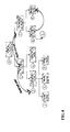
- register FIELD2 This register is put in the structure together with the register properties of this register. As there is no left most child of this register the right brother of the register FIELD1 is taken into account, register FIELD2. Register Field 2 is put in the structure together with the register properties of this register. Further, as there is no left most child of this register FIELD2 the right brother of the register FIELD2 is taken into account, register BUFFERO. Register Buffer 0 is put in the structure together with the register properties of this register. As there are ten similar registers BUFFER0..9, the number of repetition indicator PPTNBR within the register properties is set at the value 10.
- the memory of the ASIC is passed through from the lowest up to the highest memory address.
- the references of the left most child LCHILD and right most brother RBROTH of each module or sub-modules are stored in the datastructure for registrating the structure of the ASIC as shown in FIG. 5. This in order to go through the structure in same way during adding data to the datastructure as during searching for data or reading data in the datastructure.
- FPGA Field Programmable Gate Array
- EPLD Erasable Programmable Logic Device
- the above described datastructure may be used in access test executed by the microprocessor. Because of the datastructure, these tests are making abstraction of the device under test, and are therefor generic for all devices. The single image of this test code allows the execution of such access tests on each testable device based on inputs derived from such datastructure dedicated to the device to be tested.
- Such an access tests of an ASIC include either one of Read/Write of multiple patterns to two registers, data-bus test, address-bus tests, device reset tests or test initial values of all registers which all are designed once.
- Return couples of register-address which address exactly differ in 1-bit, and which refer to registers with RW-bits.
- the amount of returned couples is based on the width of the address-bus.
Landscapes
- Engineering & Computer Science (AREA)
- General Engineering & Computer Science (AREA)
- General Physics & Mathematics (AREA)
- Physics & Mathematics (AREA)
- Theoretical Computer Science (AREA)
- Quality & Reliability (AREA)
- Computer Hardware Design (AREA)
- Techniques For Improving Reliability Of Storages (AREA)
- Test And Diagnosis Of Digital Computers (AREA)
- Memory System Of A Hierarchy Structure (AREA)
- Mobile Radio Communication Systems (AREA)
- Debugging And Monitoring (AREA)
- Executing Machine-Instructions (AREA)
Priority Applications (5)
| Application Number | Priority Date | Filing Date | Title |
|---|---|---|---|
| DE60209201T DE60209201T2 (de) | 2002-10-28 | 2002-10-28 | Verfahren zum Speichern von Registereigenschaften in einer Datenstruktur und dazugehörige Datenstruktur |
| AT02292677T ATE317982T1 (de) | 2002-10-28 | 2002-10-28 | Verfahren zum speichern von registereigenschaften in einer datenstruktur und dazugehörige datenstruktur |
| ES02292677T ES2253503T3 (es) | 2002-10-28 | 2002-10-28 | Metodo para almacenar propiedades de registro en una estructura de datos y estructura de datos relacionada. |
| EP02292677A EP1416290B1 (de) | 2002-10-28 | 2002-10-28 | Verfahren zum Speichern von Registereigenschaften in einer Datenstruktur und dazugehörige Datenstruktur |
| US10/692,681 US7346749B2 (en) | 2002-10-28 | 2003-10-27 | Method for storing register properties in a datastructure and related datastructure |
Applications Claiming Priority (1)
| Application Number | Priority Date | Filing Date | Title |
|---|---|---|---|
| EP02292677A EP1416290B1 (de) | 2002-10-28 | 2002-10-28 | Verfahren zum Speichern von Registereigenschaften in einer Datenstruktur und dazugehörige Datenstruktur |
Publications (2)
| Publication Number | Publication Date |
|---|---|
| EP1416290A1 true EP1416290A1 (de) | 2004-05-06 |
| EP1416290B1 EP1416290B1 (de) | 2006-02-15 |
Family
ID=32088069
Family Applications (1)
| Application Number | Title | Priority Date | Filing Date |
|---|---|---|---|
| EP02292677A Expired - Lifetime EP1416290B1 (de) | 2002-10-28 | 2002-10-28 | Verfahren zum Speichern von Registereigenschaften in einer Datenstruktur und dazugehörige Datenstruktur |
Country Status (5)
| Country | Link |
|---|---|
| US (1) | US7346749B2 (de) |
| EP (1) | EP1416290B1 (de) |
| AT (1) | ATE317982T1 (de) |
| DE (1) | DE60209201T2 (de) |
| ES (1) | ES2253503T3 (de) |
Families Citing this family (2)
| Publication number | Priority date | Publication date | Assignee | Title |
|---|---|---|---|---|
| US7827324B2 (en) * | 2006-09-20 | 2010-11-02 | Integrated Device Technology Inc. | Method of handling flow control in daisy-chain protocols |
| US10990664B2 (en) * | 2017-11-20 | 2021-04-27 | International Business Machines Corporation | Eliminating and reporting kernel instruction alteration |
Citations (3)
| Publication number | Priority date | Publication date | Assignee | Title |
|---|---|---|---|---|
| US4450560A (en) * | 1981-10-09 | 1984-05-22 | Teradyne, Inc. | Tester for LSI devices and memory devices |
| US5243274A (en) * | 1992-08-07 | 1993-09-07 | Westinghouse Electric Corp. | Asic tester |
| US6003150A (en) * | 1996-02-02 | 1999-12-14 | Lucent Technologies Inc. | Method for testing field programmable gate arrays |
Family Cites Families (5)
| Publication number | Priority date | Publication date | Assignee | Title |
|---|---|---|---|---|
| US5812416A (en) * | 1996-07-18 | 1998-09-22 | Lsi Logic Corporation | Integrated circuit design decomposition |
| US6120551A (en) * | 1997-09-29 | 2000-09-19 | Xilinx, Inc. | Hardwire logic device emulating an FPGA |
| US6148432A (en) * | 1997-11-17 | 2000-11-14 | Micron Technology, Inc. | Inserting buffers between modules to limit changes to inter-module signals during ASIC design and synthesis |
| US6102963A (en) * | 1997-12-29 | 2000-08-15 | Vantis Corporation | Electrically erasable and reprogrammable, nonvolatile integrated storage device with in-system programming and verification (ISPAV) capabilities for supporting in-system reconfiguring of PLD's |
| JP3809727B2 (ja) * | 1998-06-17 | 2006-08-16 | 富士ゼロックス株式会社 | 情報処理システム、回路情報管理方法および回路情報記憶装置 |
-
2002
- 2002-10-28 ES ES02292677T patent/ES2253503T3/es not_active Expired - Lifetime
- 2002-10-28 AT AT02292677T patent/ATE317982T1/de not_active IP Right Cessation
- 2002-10-28 EP EP02292677A patent/EP1416290B1/de not_active Expired - Lifetime
- 2002-10-28 DE DE60209201T patent/DE60209201T2/de not_active Expired - Lifetime
-
2003
- 2003-10-27 US US10/692,681 patent/US7346749B2/en not_active Expired - Lifetime
Patent Citations (3)
| Publication number | Priority date | Publication date | Assignee | Title |
|---|---|---|---|---|
| US4450560A (en) * | 1981-10-09 | 1984-05-22 | Teradyne, Inc. | Tester for LSI devices and memory devices |
| US5243274A (en) * | 1992-08-07 | 1993-09-07 | Westinghouse Electric Corp. | Asic tester |
| US6003150A (en) * | 1996-02-02 | 1999-12-14 | Lucent Technologies Inc. | Method for testing field programmable gate arrays |
Non-Patent Citations (1)
| Title |
|---|
| YAMAGUCHI T ET AL: "AN EFFICIENT METHOD FOR COMPRESSING TEST DATA", PROCEEDINGS OF THE INTERNATIONAL TEST CONFERENCE. ITC '97. WASHINGTON, DC, NOV. 1 - 6, 1997, INTERNATIONAL TEST CONFERENCE, NEW YORK, NY: IEEE, US, vol. CONF. 28, 1 November 1997 (1997-11-01), pages 79 - 88, XP000800314, ISBN: 0-7803-4210-0 * |
Also Published As
| Publication number | Publication date |
|---|---|
| DE60209201T2 (de) | 2006-11-16 |
| US7346749B2 (en) | 2008-03-18 |
| ATE317982T1 (de) | 2006-03-15 |
| ES2253503T3 (es) | 2006-06-01 |
| DE60209201D1 (de) | 2006-04-20 |
| US20040153820A1 (en) | 2004-08-05 |
| EP1416290B1 (de) | 2006-02-15 |
Similar Documents
| Publication | Publication Date | Title |
|---|---|---|
| US6425109B1 (en) | High level automatic core configuration | |
| EP2216722A2 (de) | Divers procédés et appareil pour la cartographie configurable de régions d'adresse sur une ou plusieurs cibles agrégées | |
| US6691287B2 (en) | Functional verification system | |
| CN116956801B (zh) | 芯片验证方法、装置、计算机设备和存储介质 | |
| US6701494B2 (en) | Method of using testbench tests to avoid task collisions in hardware description language | |
| JP2004519041A (ja) | 効率的なデータロード及びアンロードのために統合されるパケット基準のプロトコル論理を用いるハードウェア支援設計検証システム | |
| US8230263B2 (en) | Automated specification based functional test generation infrastructure | |
| US6845440B2 (en) | System for preventing memory usage conflicts when generating and merging computer architecture test cases | |
| US20050091028A1 (en) | Simulator and simulation method | |
| US6629297B2 (en) | Tracing the change of state of a signal in a functional verification system | |
| US20030237032A1 (en) | Method for electronically testing memory modules | |
| EP1416290B1 (de) | Verfahren zum Speichern von Registereigenschaften in einer Datenstruktur und dazugehörige Datenstruktur | |
| CN117008967A (zh) | 一种uvm ral寄存器模型生成方法、装置及电子设备 | |
| CN118133742B (zh) | 位流测试方法、装置、计算机设备、存储介质及程序产品 | |
| US6813599B1 (en) | Efficient memory structure simulation for sequential circuit design verification | |
| US6470480B2 (en) | Tracing different states reached by a signal in a functional verification system | |
| CN116861829B (zh) | 用于定位逻辑系统设计中错误的方法、电子设备 | |
| US6480988B2 (en) | Functional verification of both cycle-based and non-cycle based designs | |
| US6721937B2 (en) | Method and system for automated processor register instantiation | |
| Mahdiany et al. | A hardware accelerator for DSP system design: University of Tehran DSP Hardware Emulator (UTDHE) | |
| CN116578491A (zh) | 一种基于组件封装的动态表单测试方法、系统及电子设备 | |
| CN100389425C (zh) | 实现数模混合型集成电路验证的方法及装置 | |
| US6804803B2 (en) | Method for testing integrated logic circuits | |
| US11966633B1 (en) | Control algorithm generator for non-volatile memory module | |
| US20020120907A1 (en) | Run-time controller in a functional verification system |
Legal Events
| Date | Code | Title | Description |
|---|---|---|---|
| PUAI | Public reference made under article 153(3) epc to a published international application that has entered the european phase |
Free format text: ORIGINAL CODE: 0009012 |
|
| AK | Designated contracting states |
Kind code of ref document: A1 Designated state(s): AT BE BG CH CY CZ DE DK EE ES FI FR GB GR IE IT LI LU MC NL PT SE SK TR |
|
| AX | Request for extension of the european patent |
Extension state: AL LT LV MK RO SI |
|
| 17P | Request for examination filed |
Effective date: 20041108 |
|
| AKX | Designation fees paid |
Designated state(s): AT BE BG CH CY CZ DE DK EE ES FI FR GB GR IE IT LI LU MC NL PT SE SK TR |
|
| 17Q | First examination report despatched |
Effective date: 20050121 |
|
| GRAP | Despatch of communication of intention to grant a patent |
Free format text: ORIGINAL CODE: EPIDOSNIGR1 |
|
| GRAS | Grant fee paid |
Free format text: ORIGINAL CODE: EPIDOSNIGR3 |
|
| GRAA | (expected) grant |
Free format text: ORIGINAL CODE: 0009210 |
|
| AK | Designated contracting states |
Kind code of ref document: B1 Designated state(s): AT BE BG CH CY CZ DE DK EE ES FI FR GB GR IE IT LI LU MC NL PT SE SK TR |
|
| PG25 | Lapsed in a contracting state [announced via postgrant information from national office to epo] |
Ref country code: IT Free format text: LAPSE BECAUSE OF FAILURE TO SUBMIT A TRANSLATION OF THE DESCRIPTION OR TO PAY THE FEE WITHIN THE PRESCRIBED TIME-LIMIT;WARNING: LAPSES OF ITALIAN PATENTS WITH EFFECTIVE DATE BEFORE 2007 MAY HAVE OCCURRED AT ANY TIME BEFORE 2007. THE CORRECT EFFECTIVE DATE MAY BE DIFFERENT FROM THE ONE RECORDED. Effective date: 20060215 Ref country code: SK Free format text: LAPSE BECAUSE OF FAILURE TO SUBMIT A TRANSLATION OF THE DESCRIPTION OR TO PAY THE FEE WITHIN THE PRESCRIBED TIME-LIMIT Effective date: 20060215 Ref country code: NL Free format text: LAPSE BECAUSE OF FAILURE TO SUBMIT A TRANSLATION OF THE DESCRIPTION OR TO PAY THE FEE WITHIN THE PRESCRIBED TIME-LIMIT Effective date: 20060215 Ref country code: BE Free format text: LAPSE BECAUSE OF FAILURE TO SUBMIT A TRANSLATION OF THE DESCRIPTION OR TO PAY THE FEE WITHIN THE PRESCRIBED TIME-LIMIT Effective date: 20060215 Ref country code: FI Free format text: LAPSE BECAUSE OF FAILURE TO SUBMIT A TRANSLATION OF THE DESCRIPTION OR TO PAY THE FEE WITHIN THE PRESCRIBED TIME-LIMIT Effective date: 20060215 Ref country code: AT Free format text: LAPSE BECAUSE OF FAILURE TO SUBMIT A TRANSLATION OF THE DESCRIPTION OR TO PAY THE FEE WITHIN THE PRESCRIBED TIME-LIMIT Effective date: 20060215 Ref country code: CH Free format text: LAPSE BECAUSE OF FAILURE TO SUBMIT A TRANSLATION OF THE DESCRIPTION OR TO PAY THE FEE WITHIN THE PRESCRIBED TIME-LIMIT Effective date: 20060215 Ref country code: LI Free format text: LAPSE BECAUSE OF FAILURE TO SUBMIT A TRANSLATION OF THE DESCRIPTION OR TO PAY THE FEE WITHIN THE PRESCRIBED TIME-LIMIT Effective date: 20060215 |
|
| REG | Reference to a national code |
Ref country code: GB Ref legal event code: FG4D Ref country code: CH Ref legal event code: EP |
|
| REG | Reference to a national code |
Ref country code: IE Ref legal event code: FG4D |
|
| REF | Corresponds to: |
Ref document number: 60209201 Country of ref document: DE Date of ref document: 20060420 Kind code of ref document: P |
|
| PG25 | Lapsed in a contracting state [announced via postgrant information from national office to epo] |
Ref country code: BG Free format text: LAPSE BECAUSE OF FAILURE TO SUBMIT A TRANSLATION OF THE DESCRIPTION OR TO PAY THE FEE WITHIN THE PRESCRIBED TIME-LIMIT Effective date: 20060515 Ref country code: SE Free format text: LAPSE BECAUSE OF FAILURE TO SUBMIT A TRANSLATION OF THE DESCRIPTION OR TO PAY THE FEE WITHIN THE PRESCRIBED TIME-LIMIT Effective date: 20060515 Ref country code: DK Free format text: LAPSE BECAUSE OF FAILURE TO SUBMIT A TRANSLATION OF THE DESCRIPTION OR TO PAY THE FEE WITHIN THE PRESCRIBED TIME-LIMIT Effective date: 20060515 |
|
| REG | Reference to a national code |
Ref country code: ES Ref legal event code: FG2A Ref document number: 2253503 Country of ref document: ES Kind code of ref document: T3 |
|
| PG25 | Lapsed in a contracting state [announced via postgrant information from national office to epo] |
Ref country code: PT Free format text: LAPSE BECAUSE OF FAILURE TO SUBMIT A TRANSLATION OF THE DESCRIPTION OR TO PAY THE FEE WITHIN THE PRESCRIBED TIME-LIMIT Effective date: 20060717 |
|
| NLV1 | Nl: lapsed or annulled due to failure to fulfill the requirements of art. 29p and 29m of the patents act | ||
| REG | Reference to a national code |
Ref country code: CH Ref legal event code: PL |
|
| ET | Fr: translation filed | ||
| PG25 | Lapsed in a contracting state [announced via postgrant information from national office to epo] |
Ref country code: IE Free format text: LAPSE BECAUSE OF NON-PAYMENT OF DUE FEES Effective date: 20061031 Ref country code: MC Free format text: LAPSE BECAUSE OF NON-PAYMENT OF DUE FEES Effective date: 20061031 |
|
| PLBE | No opposition filed within time limit |
Free format text: ORIGINAL CODE: 0009261 |
|
| STAA | Information on the status of an ep patent application or granted ep patent |
Free format text: STATUS: NO OPPOSITION FILED WITHIN TIME LIMIT |
|
| 26N | No opposition filed |
Effective date: 20061116 |
|
| PG25 | Lapsed in a contracting state [announced via postgrant information from national office to epo] |
Ref country code: CZ Free format text: LAPSE BECAUSE OF FAILURE TO SUBMIT A TRANSLATION OF THE DESCRIPTION OR TO PAY THE FEE WITHIN THE PRESCRIBED TIME-LIMIT Effective date: 20060215 Ref country code: GR Free format text: LAPSE BECAUSE OF FAILURE TO SUBMIT A TRANSLATION OF THE DESCRIPTION OR TO PAY THE FEE WITHIN THE PRESCRIBED TIME-LIMIT Effective date: 20060516 |
|
| PG25 | Lapsed in a contracting state [announced via postgrant information from national office to epo] |
Ref country code: EE Free format text: LAPSE BECAUSE OF FAILURE TO SUBMIT A TRANSLATION OF THE DESCRIPTION OR TO PAY THE FEE WITHIN THE PRESCRIBED TIME-LIMIT Effective date: 20060215 |
|
| PG25 | Lapsed in a contracting state [announced via postgrant information from national office to epo] |
Ref country code: LU Free format text: LAPSE BECAUSE OF NON-PAYMENT OF DUE FEES Effective date: 20061028 Ref country code: TR Free format text: LAPSE BECAUSE OF FAILURE TO SUBMIT A TRANSLATION OF THE DESCRIPTION OR TO PAY THE FEE WITHIN THE PRESCRIBED TIME-LIMIT Effective date: 20060215 |
|
| PG25 | Lapsed in a contracting state [announced via postgrant information from national office to epo] |
Ref country code: CY Free format text: LAPSE BECAUSE OF FAILURE TO SUBMIT A TRANSLATION OF THE DESCRIPTION OR TO PAY THE FEE WITHIN THE PRESCRIBED TIME-LIMIT Effective date: 20060215 |
|
| PGFP | Annual fee paid to national office [announced via postgrant information from national office to epo] |
Ref country code: IT Payment date: 20101025 Year of fee payment: 9 |
|
| PGFP | Annual fee paid to national office [announced via postgrant information from national office to epo] |
Ref country code: ES Payment date: 20101025 Year of fee payment: 9 |
|
| PG25 | Lapsed in a contracting state [announced via postgrant information from national office to epo] |
Ref country code: IT Free format text: LAPSE BECAUSE OF NON-PAYMENT OF DUE FEES Effective date: 20111028 |
|
| REG | Reference to a national code |
Ref country code: ES Ref legal event code: FD2A Effective date: 20131022 |
|
| PG25 | Lapsed in a contracting state [announced via postgrant information from national office to epo] |
Ref country code: ES Free format text: LAPSE BECAUSE OF NON-PAYMENT OF DUE FEES Effective date: 20111029 |
|
| REG | Reference to a national code |
Ref country code: FR Ref legal event code: GC Effective date: 20140717 |
|
| REG | Reference to a national code |
Ref country code: FR Ref legal event code: RG Effective date: 20141016 |
|
| REG | Reference to a national code |
Ref country code: FR Ref legal event code: PLFP Year of fee payment: 14 |
|
| REG | Reference to a national code |
Ref country code: FR Ref legal event code: PLFP Year of fee payment: 15 |
|
| REG | Reference to a national code |
Ref country code: FR Ref legal event code: PLFP Year of fee payment: 16 |
|
| PGFP | Annual fee paid to national office [announced via postgrant information from national office to epo] |
Ref country code: FR Payment date: 20171024 Year of fee payment: 16 Ref country code: DE Payment date: 20171019 Year of fee payment: 16 |
|
| PGFP | Annual fee paid to national office [announced via postgrant information from national office to epo] |
Ref country code: GB Payment date: 20171019 Year of fee payment: 16 |
|
| REG | Reference to a national code |
Ref country code: DE Ref legal event code: R119 Ref document number: 60209201 Country of ref document: DE |
|
| REG | Reference to a national code |
Ref country code: DE Ref legal event code: R082 Ref document number: 60209201 Country of ref document: DE Representative=s name: MENZIETTI WETZEL, DE Ref country code: DE Ref legal event code: R081 Ref document number: 60209201 Country of ref document: DE Owner name: PROVENANCE ASSET GROUP LLC, PITTSFORD, US Free format text: FORMER OWNER: ALCATEL LUCENT, PARIS, FR |
|
| GBPC | Gb: european patent ceased through non-payment of renewal fee |
Effective date: 20181028 |
|
| PG25 | Lapsed in a contracting state [announced via postgrant information from national office to epo] |
Ref country code: DE Free format text: LAPSE BECAUSE OF NON-PAYMENT OF DUE FEES Effective date: 20190501 |
|
| PG25 | Lapsed in a contracting state [announced via postgrant information from national office to epo] |
Ref country code: FR Free format text: LAPSE BECAUSE OF NON-PAYMENT OF DUE FEES Effective date: 20181031 |
|
| REG | Reference to a national code |
Ref country code: GB Ref legal event code: 732E Free format text: REGISTERED BETWEEN 20190829 AND 20190904 |
|
| PG25 | Lapsed in a contracting state [announced via postgrant information from national office to epo] |
Ref country code: GB Free format text: LAPSE BECAUSE OF NON-PAYMENT OF DUE FEES Effective date: 20181028 |