EP1420244A2 - Système de contrôle video utilisant une illumination multispectrale par diodes électroluminescentes - Google Patents
Système de contrôle video utilisant une illumination multispectrale par diodes électroluminescentes Download PDFInfo
- Publication number
- EP1420244A2 EP1420244A2 EP04000727A EP04000727A EP1420244A2 EP 1420244 A2 EP1420244 A2 EP 1420244A2 EP 04000727 A EP04000727 A EP 04000727A EP 04000727 A EP04000727 A EP 04000727A EP 1420244 A2 EP1420244 A2 EP 1420244A2
- Authority
- EP
- European Patent Office
- Prior art keywords
- video
- array
- light
- inspection
- engineered
- Prior art date
- Legal status (The legal status is an assumption and is not a legal conclusion. Google has not performed a legal analysis and makes no representation as to the accuracy of the status listed.)
- Withdrawn
Links
Images


Classifications
-
- G—PHYSICS
- G01—MEASURING; TESTING
- G01N—INVESTIGATING OR ANALYSING MATERIALS BY DETERMINING THEIR CHEMICAL OR PHYSICAL PROPERTIES
- G01N21/00—Investigating or analysing materials by the use of optical means, i.e. using sub-millimetre waves, infrared, visible or ultraviolet light
- G01N21/84—Systems specially adapted for particular applications
- G01N21/88—Investigating the presence of flaws or contamination
- G01N21/89—Investigating the presence of flaws or contamination in moving material, e.g. running paper or textiles
- G01N21/8901—Optical details; Scanning details
-
- G—PHYSICS
- G01—MEASURING; TESTING
- G01N—INVESTIGATING OR ANALYSING MATERIALS BY DETERMINING THEIR CHEMICAL OR PHYSICAL PROPERTIES
- G01N21/00—Investigating or analysing materials by the use of optical means, i.e. using sub-millimetre waves, infrared, visible or ultraviolet light
- G01N21/84—Systems specially adapted for particular applications
- G01N21/88—Investigating the presence of flaws or contamination
- G01N21/8806—Specially adapted optical and illumination features
-
- G—PHYSICS
- G01—MEASURING; TESTING
- G01N—INVESTIGATING OR ANALYSING MATERIALS BY DETERMINING THEIR CHEMICAL OR PHYSICAL PROPERTIES
- G01N21/00—Investigating or analysing materials by the use of optical means, i.e. using sub-millimetre waves, infrared, visible or ultraviolet light
- G01N21/84—Systems specially adapted for particular applications
- G01N21/88—Investigating the presence of flaws or contamination
- G01N21/89—Investigating the presence of flaws or contamination in moving material, e.g. running paper or textiles
- G01N21/8901—Optical details; Scanning details
- G01N21/8903—Optical details; Scanning details using a multiple detector array
-
- H—ELECTRICITY
- H04—ELECTRIC COMMUNICATION TECHNIQUE
- H04N—PICTORIAL COMMUNICATION, e.g. TELEVISION
- H04N7/00—Television systems
- H04N7/18—Closed-circuit television [CCTV] systems, i.e. systems in which the video signal is not broadcast
- H04N7/181—Closed-circuit television [CCTV] systems, i.e. systems in which the video signal is not broadcast for receiving images from a plurality of remote sources
-
- H—ELECTRICITY
- H04—ELECTRIC COMMUNICATION TECHNIQUE
- H04N—PICTORIAL COMMUNICATION, e.g. TELEVISION
- H04N7/00—Television systems
- H04N7/18—Closed-circuit television [CCTV] systems, i.e. systems in which the video signal is not broadcast
- H04N7/188—Capturing isolated or intermittent images triggered by the occurrence of a predetermined event, e.g. an object reaching a predetermined position
-
- G—PHYSICS
- G01—MEASURING; TESTING
- G01N—INVESTIGATING OR ANALYSING MATERIALS BY DETERMINING THEIR CHEMICAL OR PHYSICAL PROPERTIES
- G01N21/00—Investigating or analysing materials by the use of optical means, i.e. using sub-millimetre waves, infrared, visible or ultraviolet light
- G01N21/84—Systems specially adapted for particular applications
- G01N21/88—Investigating the presence of flaws or contamination
- G01N21/8806—Specially adapted optical and illumination features
- G01N2021/8835—Adjustable illumination, e.g. software adjustable screen
-
- G—PHYSICS
- G01—MEASURING; TESTING
- G01N—INVESTIGATING OR ANALYSING MATERIALS BY DETERMINING THEIR CHEMICAL OR PHYSICAL PROPERTIES
- G01N21/00—Investigating or analysing materials by the use of optical means, i.e. using sub-millimetre waves, infrared, visible or ultraviolet light
- G01N21/84—Systems specially adapted for particular applications
- G01N21/88—Investigating the presence of flaws or contamination
- G01N21/8806—Specially adapted optical and illumination features
- G01N2021/8845—Multiple wavelengths of illumination or detection
-
- G—PHYSICS
- G01—MEASURING; TESTING
- G01N—INVESTIGATING OR ANALYSING MATERIALS BY DETERMINING THEIR CHEMICAL OR PHYSICAL PROPERTIES
- G01N21/00—Investigating or analysing materials by the use of optical means, i.e. using sub-millimetre waves, infrared, visible or ultraviolet light
- G01N21/84—Systems specially adapted for particular applications
- G01N21/88—Investigating the presence of flaws or contamination
- G01N21/8851—Scan or image signal processing specially adapted therefor, e.g. for scan signal adjustment, for detecting different kinds of defects, for compensating for structures, markings, edges
- G01N2021/8887—Scan or image signal processing specially adapted therefor, e.g. for scan signal adjustment, for detecting different kinds of defects, for compensating for structures, markings, edges based on image processing techniques
-
- G—PHYSICS
- G01—MEASURING; TESTING
- G01N—INVESTIGATING OR ANALYSING MATERIALS BY DETERMINING THEIR CHEMICAL OR PHYSICAL PROPERTIES
- G01N2201/00—Features of devices classified in G01N21/00
- G01N2201/06—Illumination; Optics
- G01N2201/062—LED's
- G01N2201/0621—Supply
Definitions
- This application pertains to the art of machine vision and more particularly to high speed automated video inspection.
- the invention is particularly applicable to automated video inspection of continuous web-like materials such as cloth, paper, MYLAR, sheet metal, etc., and will be described with particular reference thereto, although it will be appreciated that the invention has broader applications such as in the inspection of any continuously moving specimen whether discrete or continuous in which the specimen passes through the field of view of an associated inspection camera and in systems utilizing relatively low illumination levels.
- Machine vision systems have obtained an established presence in industry to accomplish high speed video inspections. Such machine vision systems are generally comprised of a lighting system to illuminate a specimen and a camera for sensing light reflected therefrom. A digitized image is formed from an image received by the camera. Data representative of this image is then utilized for determining acceptability of the specimen in view of preselected physical characteristics thereof.
- Substantial product is manufactured as a continuous stream of webbed or sheet-like material. While the aforementioned systems are adequate for a number of inspections, they provide no means for acquiring a consistently detailed inspection image of a continuous stream of fast moving web material. Earlier attempts to achieve automated inspection of such materials relied upon line scan cameras with continuous illumination. Stroboscopic systems were also utilized but required intense illumination periods. It was therefore desirable that a system be provided which allows for detailed high speed video inspection on a continuous stream of web material or which utilizes heretofore inadequate lighting intensities with improved image integrity and which exhibits robustness over a wide range of specimens.
- TDI time delay integration
- TDI inspection techniques center on numeric processing, rather than lighting technique. Previous techniques are conducive to some "smearing" of each linear cross-section image. Also, often times different grades of webbing or even entirely different webbing materials may at various times be inspected by the same system. Similarly, non-webbing systems often encounter markedly different specimens at different times. Differences in reflectivity in these situations require compensation. This is typically accomplished by compensation in the inspection algorithm software. Even this is limited given that absolute light sensitivity limits are inherent in CCDs, and once a sensitivity threshold has been exceeded, information is lost and compensation is not possible.
- First generation light emitting diodes provided a high portion of their output in the infrared spectrum, which is to be expected from the physical characteristics of the semiconductor substrate from which they were fabricated. Since then, different semiconductor substrates have been utilized to generate light having wavelength frequency that is higher than infrared. Expectedly, first visible LEDs were primarily red in color.
- charge-coupled devices are also fabricated in silicon. Accordingly, their maximum sensitivity is in the infrared area of the spectrum, analogously to the maximum spectral light output of silicon. Accordingly, first generation video illumination, utilizing LEDs, was with infrared lighting. Second generation lighting employed visible red LEDs. Recent advances and LEDs have provided other colors with a usable amount of energy. Further, advances in CCD technology have allowed for increased sensitivity to different illumination spectra.
- the present invention contemplates a new and improved TDI video inspection and engineered lighting system which overcomes all the above-referred problems, and others, and provides a video inspection system allowing for continuous inspection of a stream of web materials or other specimens with improved integrity utilizing multiple or selectable color spectra.
- an engineered lighting video inspection system includes an array of light emitting elements formed of LEDs of multiple spectral characteristics.
- the light emitting elements of the array are secured such that they are controllable in one or more discrete subsets.
- a signal representative of a linear velocity of an associated specimen relative to the array is provided to a controller.
- the controller functions to selectively enable the light emitting element for a short time period.
- Light of the array of light emitting elements is, after exposure to the specimen, communicated to a light sensitive transducer array, the rows of which are synchronized to a continuous webbing material or other specimen.
- backlighting is provided by a selected plurality of lighting elements disposed on a side of the specimen opposite of the light sensitive transducer.
- An advantage of the present invention is the provision of a video inspection system for accomplishing detailed inspection of a continuous stream of sheet or web-like materials or other specimens when the specimens are of varying or various colors.
- Another advantage of the present invention is the provision of an inspection system employing selected illumination spectra.
- Another advantage of the present invention is the provision of a video inspection system for inspecting a continuous stream of sheet or web-like materials or other specimen using multiple cameras and a concurrent illumination.
- Another advantage of the present invention is the provision of a video inspection system for accomplishing detailed inspection of continuous stream of sheet or web-like materials or other specimen while allowing for inspection of flaws which are not discernable by a particular illumination spectrum.
- Another advantage of the present invention is the provision of a system which allows for obtaining a frozen image of sequential areas of the web material with the multiple or selective spectral illumination noted above.
- Yet another advantage of the present invention is the provision of a system which allows for accumulation of multiple image data sets from selected areas of a continuous stream of web materials to accomplish improved high speed, detailed video inspection thereof with relatively low light levels of multiple or selective spectral illumination as noted above, in a system adaptable to a wide range of webbing materials.
- Yet another advantage of the present invention is the provision of an inspection system for improved inspection of discrete images.
- Yet another advantage is the provision of an inspection system which achieves an improved signal-to-noise ratio for captured images.
- Yet another advantage is the provision of an inspection system employing lighting having improved characteristics, consistency, stability and reliability.
- FIGURE 1 illustrates an engineered video inspection system A which includes an engineered illumination system or means B, a data acquisition system or means C, and a computer system or means D.
- the illumination system B is formed from an array of a plurality of light emitting elements 10 preferably comprised of solid-state lighting elements, such as a plurality of light emitting diodes ("LEDs").
- LEDs light emitting diodes
- Light emitting diodes advantageously provide a fast responsive, long lived, and consistent light output.
- the light emitting diodes are focused to a generally narrow beam or cone of light emanating therefrom, which cone has a generally selected angle.
- a similar effect to a focused LEDs may be realized by employing a wider beam coupled with a decreased distance between the LEDs and a specimen.
- Typical, focused, light emitting diodes include a bullet-shaped casing which functions as a lens to project the narrow beam or cone of light therefrom. What focus is used, the arrangement of the devices, and the angles of illumination chosen is extremely application dependent. Conventionally available focused light emitting diodes have a beam of light generally wide angle (20° at the vertex), or 10° from a perpendicular centerline thereof. The subject system employs selection of LED angles which are highly application dependent. The more focused LEDs allow for concentration of a maximum amount of light from a given LED in a small area while concurrently maintaining uniformity in illumination. This also provides for a higher intensity of illumination on a specified area, subjecting the area to individual controllability of intensities and angles thereacross to controllability of individual or groups or subsets of light emitting diodes.
- Light emitting diodes may be pulsed at extremely high currents provided that the duration is sufficiently small to prevent heat build-up which may damage the PN junction forming the diode. It is found that a duration in the range of 1 to 200 microseconds allows for provisions of such high currents with no or nominal damage to the LED. As will be described further below, it will be seen that this duration is also sufficient to "freeze" the image of a rapidly moving specimen so that a still image may be captured therefrom.
- 240 scan lines are implemented in the CCD array. Accordingly, 240 pulses and 240 exposures are integrated for each linear cross section of a specimen.
- the subject system concurrently flashes all or some of the diodes 10 in a duration of approximately 4 ⁇ sec given the light accumulation properties of TDI.
- Each LED is suitably supplied with between 1 mA and 500 Ma of current during this duration.
- a value of 73 mA has proven acceptable. Suitable power supplies to accomplish such pulsing are well within the understanding of one of ordinary skill in the art and will not be described herein.
- the 4 ⁇ sec time is selected to advantageously provide low duty cycle compared to the typical horizontal scan time for NTSC video signals.
- a 15.75 Khz scan rate provides a 63 ⁇ sec horizontal scan time. Accordingly, the 4 ⁇ sec pulse provides a 4/63 duty cycle. This particular rate with actual duty cycle is proportioned to a scan rate implemented for a particular application.
- the light emitting diodes 10 are secured by a bracket or securing means 12 in a generally hemi-cylindrical array 16.
- Such an array structure advantageously provides generally uniform illumination to a rectangular light field 14.
- This structure is suitably fabricated from a flexible printed circuit board portion secured to two hemispherical printed circuit board end portions. LEDs are mounted on the interior portion of the array 16, and are preferably placed as closely as possible to one another to maximize illumination and minimize transitions therebetween, thereby forming a more uniform light field.
- this particular structure is employed in the preferred embodiment, it will be appreciated that various other array structures may be employed for illumination of various specimens.
- Angled lighting i.e., lighting which communicated from one or more LEDS to a specimen and is reflected off the specimen surface to a camera with a stated angle at less than 180°, is advantageously employed for improved detection of certain surface defects.
- Such systems may optionally implement a perspective correcting lens to maintain image characteristics through the progression within the CCD array.
- a perspective correcting lens allows for direction of light from an array to a specimen at a non-perpendicular angle while negating artifacts which would otherwise result from such an orientation. For example, angled (non-perpendicular) light from a rectangular array which illuminates a specimen causes a trapezoidal illumination area.
- the video receptor of the resultant image is similarly distorted. The reflected image of the lens itself can thus be eliminated by use of a perspective correcting lens when highly reflective materials are being inspected thus allowing the desired degree of homogeneity in the imaged web.
- the light emitting diodes 10 are also suitably subdivided into a plurality of groups or subsets 20. Light emitting diodes of each of the subsets 20 are controlled together via connections 22 with a power supply and junction box 24. Grouping of the light emitting elements provides a means with which control of the intensity along selected subsections of an associated specimen may be made or by which selected angles of illumination may be provided. Such structure also provides an ability to compensate for degrading or burned-out elements by boosting output of surrounding elements. It further provides for reduction of reflected light reaching any given region of the camera sensor.
- a portion of the light emitting elements 10 is formed into a backlight array 26.
- Backlighting is often advantageously employed for inspection of light transmissive specimens or subportions of specimens.
- the backlight array 26 is secured so as to be generally planar. Such a planar orientation is generally best suited for backlighting applications, although it will be appreciated that various other orientations may be successfully utilized.
- light emitting diodes of the backlight array 26 are suitably formed into a plurality of subsets 28, interconnected with power supply and junction box 24. These connections have been omitted from FIGURE 1 for ease in illustration. Such formation of subsets provides for controllability analogous to that provided with the arrangement above-described for primary array portion 16.
- FIGURE 1 Illustrated in FIGURE 1 is a cross-sectional side view of a diffuser 30.
- the diffuser 30 is advantageously formed as a hemi-cylindrical shape to be similar to the shape of the array 16, and placed internally thereof.
- the optional diffuser functions to smooth transitions between LEDs of the array, thereby providing an even more uniform light field.
- segment 38 of a stream of webbing material which is in generally continuous motion in the direction so indicated.
- webbing material will be understood to refer to any sheet-like material, such as paper, cloth, sheet metal, plastic, laminates, and the like. It is understood that the system is also advantageously employed in discrete specimen systems. However, for simplicity descriptions herein will generally be with sole reference to webbing environments.
- a conveyor driver (not shown) continuously moves the web 38 through the light field 14 at a generally high speed. Web position is measured by a web position/velocity sensor, such as a tachometer 40. Light from light emitting diodes 10 of the primary array portion 16 is reflected from the web 38.
- Reflected light from a viewing area 42 is received through a lens 44 of a camera 46. Although only one camera is illustrated in the cross-sectional view of the figure, it will be shown below that often a plurality of cameras are advantageously employed.
- the viewing area 42 is isolated as much as possible from amount light, i.e., light not provided by light from the primary (or secondary) lighting array(s) 16 (28).
- the lens 44 of camera 46 is secured to extend slightly into the light field 14 through an aperture portion 52.
- the lens 44 is preferably formed as a "pinhole" unit to minimize image artifacts due to the camera itself. Such lens arrangements are typically less than 3 ⁇ 8" in diameter.
- the aperture portion is suitably disposed at a generally central portion of the array should one camera be utilized, and at equivalent intervals in embodiments employing a plurality of cameras.
- the subject system in its preferred embodiment, employs a TDI camera, VISIONEER 4050 manufactured by Picker International, Inc.
- the camera 46 includes a CCD array in the preferred embodiment. It will be appreciated that CCD arrays are usually M x N rectangular arrays of photosensitive transducer elements, wherein M and N are positive, non-zero integers, usually multiples of two.
- the camera of the preferred embodiment functions as 244 rows of CCD elements, each row having 610 pixels.
- the camera 46 is oriented relative to the web 40 such that each row is generally perpendicular to the direction of travel thereof.
- Typical CCD arrays are sensitive to a selected number of gray scale levels, for black and white systems, or primary colors, for color systems.
- CCD cameras allow for individual addressing of rows of transducer element thereof, analogously to the raster scan associated with conventional cathode ray tubes ("CRTs").
- CCD elements also operate as integrators which provide an electrical signal representative of an intensity of light exposed thereto over time.
- a CCD transducer element also has the ability to store light intensity data. This property is useful for achieving a still image of a specimen or portion thereof by strobing or pulsing a light source when the moving specimen is otherwise in a generally darkened field of view.
- the camera 46 also advantageously includes an adjustment system 48 for control of focus, planetary, vertical, horizontal properties. Orthogonality must be maintained between sensor and inspected material. Such adjustment may be done manually, or in conjunction with signals provided by the digital computer system D by data communication camera sync and control lines.
- Image data acquired from camera 46 is communicated, through video signal line 60, to the digital computer system D, and more particularly to the computer 62 thereof.
- the computer 62 includes a central processor (CPU), memory, an I/O unit, and a suitable software and junction box 24 and with the webbing speed sensor 40.
- the computer 62 determine acceptability of the specimens by a comparison of digitized image data with data representative of acceptability.
- FIGURE 2 illustrates an embodiment in which three cameras, 46a, 46b, and 46c are oriented relative to webbing material 38 in a mutual linear relationship. Respective viewing areas of the cameras are linearly aligned to provided a cross-section of the entire specimen surface. Securing the cameras in this manner provides an extended viewing area 42 sufficient to encompass a cross-section of a relatively wide webbing.
- FIGURE 3 illustrates an embodiment in which camera 46 is itself formed from a plurality of cameras.
- light from a specimen is communicated to a partially silvered mirror 70.
- a portion passes directly to lens 44' of camera 46'.
- a second light portion is reflected from mirror 72 to lens 44" of camera 46".
- Implementation of a dual or multiple camera structure, such as that illustrated by FIGURE 3, advantageously provides a means by which selected portions of the specimen may be provided with either increased resolution to accomplish specialized inspections or optical filtering thereon. For example, a seam or scoring in the inspected web material might be subject to heightened scrutiny by virtue of utilization of a secondary camera element focused specifically thereon.
- a third camera is also advantageously implemented for additional subportion analysis, as illustrated in phantom as numeral 72' in FIGURE 3.
- Lighting to each camera of such multiple camera beam-splitter environments will generally not yield as desirable a result or design because of the intense lighting required to provide enough light to each camera (when the exposure time is short and) since the splitting reduces the intensity inherently.
- FIGURES 4 and 5 a graph illustrating operation of the charge coupled devices within the camera or cameras 46 is provided.
- position is represented by the abscissa while shift time is represented by the ordinate.
- shift time is represented by the ordinate.
- a series of illuminations or light pulses are represented by the rectangles 80 of the graph.
- rows or scan lines of each are preferably synchronized between all cameras. It is also equivalent to provide multiple pulses per scan line if advantageous.
- Synchronization between the CCD and the webbing may be accomplished by control of web velocity or of CCD row increments.
- the CCD row incrementing is altered in accordance with variations in web speed by variations in shift control as described below.
- orientation of a CCD array 82 is provided.
- the digital computer system D which is illustrated with a keyboard, CRT, and mass storage media, and which includes the computer 62, receives a signal representative of web velocity from a sensor 40. This information is in turn utilized to sequence the scan of row 86 of a CCD array elements 88, via row scan selected circuitry illustrated as shift register 90. Similar sequencing is provided for each CCD array in multiple camera embodiments. The webbing progression is continuously monitored and the shift time implemented by the row select circuitry 90 is altered in accordance therewith.
- the graph of FIGURE 4 illustrates the variation and shift time in accordance with the web speed.
- step 102 data representative of web speed is obtained from tachometer 40.
- step 104 web speed data is utilized to synchronize the shift register or registers of the CCD cameras with the web speed velocity data obtained in step 102.
- step 106 the array or arrays of LEDs is pulsed for a short duration, approximately 4 ⁇ sec. in the preferred embodiment as noted above. This duration, by virtue of the synchronization with the webbing speed, is timed at the point when the previous shifting operation has settled, thereby providing the minimized smearing. Lighting intensity is also alterable in connection with this step.
- the digital computer instructs shifting of shift register 90 to cause progression of rows of the CCD array 82 towards register 92. Accordingly, at this time the contents of previous row 86N are then communicated to register 92 in step 110. This data is, in turn, communicated through image processor 94 to digital computer system D at step 112. At this stage, a suitable algorithm is performed on the data to determine acceptability of the specimen.
- Step 114 lighting intensity adjustment data is received to allow for selective control of intensity in step 106.
- Step 116 allows completed inspections to terminate at step 118 and continuing inspections to progress back to step 102.
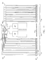
- FIGURE 7 illustrates an alternative embodiment of the primary array 16 illustrated in FIGURES 1 and 5.
- the primary array 16' is formed from a series of planar rectangular portions 16a' - 16d' and first and second planar end portions 16e' and 16f'.
- an interior portion of the array 16' contains closely packed LEDs directed to the webbing material 38'.
- This embodiment advantageously allows for fabrication of the array 16' from common, planar printed circuit board material. This orientation nonetheless provides for substantial uniform illumination over a light field 14' which encompasses a portion of the webbing 38'.
- array formats may also be utilized, which formats are dictated by properties or dimensions of the webbing material and the angles and intensities of illumination required to provide the desired qualities of the illumination. For example, hemispherical, "tiffany-lamp” style, etc. may be utilized.
- the modulated row select CCD structure provides a system with which multiple readings of a single linear subsection of a continuously moving web material may be achieved without the necessity of using a plurality of cameras or a moving camera. Data achieved by multiple acquisition provides more reliable data upon which inspection may be made. Also lighting specific to subsections of the CCD may be advantageously applied at appropriate angles and intensities.
- a plurality of illumination quanta are obtained by implementation of a plurality of LEDs 116 having a first specified wavelength range and a plurality of LEDs 118 having a generally second wavelength range, distinct from the first wavelength.
- the LEDs 116, 188 of array 10' are provided for illustration. It is to be understood that the array 10' provides an alternative embodiment to a single-color array, suitable for implementation in connection with the engineered video inspection system A and more particularly in connection with the array 20 or backlighting array 28.
- the arrangement of LEDs 116 and 118 of the embodiment of array 10' of Figure 8 provide both red and amber spectra.
- amber LEDs are available which will generate light output in the range of 700-900 millicandella/watt. While the utility and advantages, to be noted further below, from multi-spectra are achievable with any combination of LEDs, the combination of red and amber is particularly suited to inspections in connection with conventional, present-day LED and CCD components.
- significant light output from red LEDs particularly when provided with high current for a short duration, has been available in the past. More recently, the spectrum of relatively high output LEDs has progressed to the wavelengths of orange light through to amber while retaining a significant light energy output.
- the amber color, selected for the second component wavelength balances both relatively high energy output with significant distance from red to achieve utility as will be appreciated below.
- Figure 8 provides a compact physical array arrangement achieved by staggering LEDs, as evidenced between rows 122 and 124, such that a perimeter of an LED from row 24 extends into an area between perimeters of adjacent LEDs of row 22, and vice versa. This compact ordering allows for maximum light output per unit area of an array surface.
- the structure of the array 10' is further illustrated as comprising equal numbers of red LEDs 116 and amber LEDs 118.
- red LEDs 116 and amber LEDs 118 are relative intensities between spectra. That is, compensation between relative spectra intensities is suitably adjusted by varying a proportion of one spectra relative to one, or more other spectra provided by LEDs of the array to provide a base illumination.
- the base illumination is alterable by selective LED enablement as well as by varying current drive levels or "on" duration. It might be expected that LEDs have a significantly lower output or if camera sensitivity to the amber light would be lessened thereto. This is suitably addressed with a proportionally greater number of amber LEDs to red LEDs, application of a higher current to the amber LEDs, or increased "on" time of the amber LEDs, alone or in combination to balance this difference.
- multiple frequency inspection illumination provide an ability to realize additional advantages. That is, certain specimen characteristic render illumination and inspection of an entire specimen, at one time, difficult or impossible. For example, inspection of a concave specimen may require unique lighting, due to angle, orientation, disposition, or color, relative to another portion. Traditionally, such inspections were completed with multiple passes before plural inspection stations, or with repeated passes on a single inspection station.
- FIGURE 9 illustrated is a portion of the array 10', together with a sufficient segment of the video inspection system A and computer system or means D to illustrate the particulars of a modified embodiment to that described hereinabove. Also illustrated is a portion of the diffuser 30 and a modified power supply and junction box 24'. Also illustrated in FIGURE 9 are two alternative interconnections between LEDs of the array 10' and the power supply and junction box 24'. The ground or common connection to each LED is not illustrated for ease in viewing. Either or both interconnections, as illustrated by'portions 130 and 132 are suitably implemented. The portion 130 is a direct LED control for individual, or small subgroups, of LEDs as dictated by power supply and junction box 24'.
- the portion 132 illustrates a banked LED control.
- the portion 130 provide a unique control line of a grouping 134 to each LED or subgroup of LEDs.
- the group, or subgroup, of red or amber LEDs are controller via a single line 138 or line 140, respectively.
- the illustrated interconnection of the direct LED control portion 130 advantageously allows for customizable lighting, both to lighting location, intensity, and spectrum. However, a trade-off is provided by control complexity, as well as control line complexity as illustrated by control lines 134.
- the LED bank control 132 conversely, maintains relatively simplified control and wiring. However, it suffers from the spatial, spectral, and intensity flexibility of the portion 130 by requiring control of a single color. Of course, it will be appreciated that multiple LEDs may also be utilized in a single, array-wide control such that the entire array is pulsed or strobed with a single, uniform multi-chromatic light pulse.
- a specimen so illuminated by the multi-chromatic light will result in reflected (for frontal lighting) or transmitted (for backlighting) light of one or plural spectra.
- Such light is received in the embodiment of FIGURE 9 in first and second video receptors illustrated as cameras 46' and 46".
- these cameras are similar to those of camera 46, noted above.
- the camera 46' has affixed thereto a first filter 144 adapted to filter a selected wavelength, illustrated as red.
- the filter 144 intercepts light after reflection from the specimen prior to exposure of the camera 46'. Accordingly, the camera 46' would primarily be sensitive to the inspection areas which are revealed by the amber light from the LEDs 118 by virtue of filtering of the red light prior to exposure of the camera light sensitive element.
- camera 46" has affixed thereto an amber filter 146. As with the camera 46', flaws discernable by illumination of the LED 118 would be discernable from the camera 46" by virtue of filtration of the amber spectrum prior to exposure.
- FIGURE 10 a modified portion of the structure of FIGURE 10 is provided.
- Specific interconnection for control of the LEDs 10' will be understood to be similar to that described in connection with FIGURE 9. While the embodiment of FIGURE 9 employed filters, spectral separation in the embodiment of FIGURE 10 is accomplished by virtue of a lens 150 and a prism 152.
- the lens 150 serves to gather light resultant from exposure to a specimen and communicating it to the prism 152.
- prism 152 functions to provide spatial separation of polychromatic light which is a well known prism property.
- An advantage associated with prism usage is that since spectral separation is accomplished by relative indices of refraction, lessened intensity loss relative to that expected from a filter is obtained.
- FIGURE 11 yet another embodiment illustrating several, alternative structures is provided.
- a combination of a lens 150' and a diffraction grating 154 is utilized for spectral separation.
- a diffraction grating such as at 154, utilizes diffractive properties of light through a slit system to accomplish spectral separation analogously to the prism 152 of FIGURE 10.
- first and second cameras 46' and 46" are spatially separated in accordance with spectral displacement resultant from the grating 154.
- LEDs 158 of the array 10" are each multi-spectral. Presently, LEDs which are capable of providing multiple colors are available. Typically, a first signal to the LED dictates are first color while a second signal to the LED dictates the second. As with FIGURE 9, two interconnections between a further modified power supply and junction box 24" and a first LED portion 162 and a second LED portion 164 are illustrated. Again, either or both of such interconnections are suitably implemented.
- the first portion 162 provides two interconnections between each LED thereof and the power supply and junction box 24". In this way, various LEDs 158 of the array may be activated, selectively by position and/or color. As with the portion 134 of FIGURE 9, a trade off is provided in the complexity resultant to the power supply and junction box 24", as well as complexity of interconnection via connectors 168.
- the second portion 164 provides banked control analogously to the bank control of portion 132 of FIGURE 9.
- a line 168 suitably provides banked control of a first color of each LED, illustrated as green.
- line 170 provides bank control of the second color associated with each LED, red in the illustration.
- FIGURE 12 additional modifications to the subject system are described.
- illumination is provided from several sources.
- Solid-state, LED illumination is provided from a first circular ring array 200 and a second, circular ring array 202.
- the ring 200 is illustrated in cut-away form for ease in visualization.
- LEDs of the first ring array 200 are chosen so as to provide a selected wavelength range, such as amber.
- Those LEDs of the array 202 are chosen to provide a second spectrum range, such as red.
- FIGURE 12 provides additional illustration as to structured or engineered lighting. This evidences angle, intensity, and spectrum of illumination constituents.
- specific applications may dictate incorporation of various combinations of LEDs, both spectrally and relative quantities, within or between the arrays 200 and 202.
- FIGURE 12 An additional illumination example is also evidenced by FIGURE 12.
- a conventional lighting source is suitably implemented as a supplemental light generator.
- Such conventional illumination is suitably formed of incandescent, fluorescent, halogen, or intermittent duty strobe lighting such as inert gas xenon or the like, inert gas, or other similar, non solid-state junction lighting.
- Such conventional lighting sources provide multiple spectrum illumination. Therefore, this embodiment is optionally provided with a filter 210 which eliminates any undesirable light wavelength from that emanating from conventional source 206.
- a camera In conventional lighting arrangements, a camera, more specifically a lens thereof, is disposed at some point within the illumination source, such as in the middle of rings 200 and 202.
- the camera is mounted so as to have its lens axis orthogonally along a normal N of a direction of travel T of a specimen.
- This relative orientation allows for a non-distorted image of a specimen to be obtained.
- transmissive specimens which allow the camera lens to be located on the other side of the specimen.
- a perspective control lens provides well-defined optical properties to counter perspective distortions associated with off-axis placement relative to a specimen.
- a perspective control lens is illustrated generally at 216.
- Such a lens allows lens 216 to be non-orthogonally secured relative to specimen direction T.
- the lens 216 is mounted relative to the lighting such that the angle of incidence of direction I of light relative to T is equal to angle of reflection of direction R relative to T. While a single lens 216 is illustrated, it will be appreciated that multiple cameras and filters are advantageously provided, analogous to the embodiments described above. Such has been eliminated from the figure for ease in viewing.
- a power supply junction box 24 This is illustrated to demonstrate control of arrays 200 and 202, as well as conventional light source 206.
Landscapes
- Engineering & Computer Science (AREA)
- Immunology (AREA)
- Health & Medical Sciences (AREA)
- Chemical & Material Sciences (AREA)
- Analytical Chemistry (AREA)
- Biochemistry (AREA)
- General Health & Medical Sciences (AREA)
- Life Sciences & Earth Sciences (AREA)
- General Physics & Mathematics (AREA)
- Pathology (AREA)
- Physics & Mathematics (AREA)
- Multimedia (AREA)
- Signal Processing (AREA)
- Textile Engineering (AREA)
- Investigating Materials By The Use Of Optical Means Adapted For Particular Applications (AREA)
- Investigating Or Analysing Materials By Optical Means (AREA)
- Investigating, Analyzing Materials By Fluorescence Or Luminescence (AREA)
Applications Claiming Priority (3)
| Application Number | Priority Date | Filing Date | Title |
|---|---|---|---|
| US990009 | 1992-12-14 | ||
| US07/990,009 US5365084A (en) | 1991-02-20 | 1992-12-14 | Video inspection system employing multiple spectrum LED illumination |
| EP94903631A EP0729572B1 (fr) | 1992-12-14 | 1993-12-13 | Systeme de controle a video et methode d'eclairage utilisant une illumination multi-spectrale par diodes electroluminescentes |
Related Parent Applications (1)
| Application Number | Title | Priority Date | Filing Date |
|---|---|---|---|
| EP94903631A Division EP0729572B1 (fr) | 1992-12-14 | 1993-12-13 | Systeme de controle a video et methode d'eclairage utilisant une illumination multi-spectrale par diodes electroluminescentes |
Publications (2)
| Publication Number | Publication Date |
|---|---|
| EP1420244A2 true EP1420244A2 (fr) | 2004-05-19 |
| EP1420244A3 EP1420244A3 (fr) | 2005-09-14 |
Family
ID=25535656
Family Applications (2)
| Application Number | Title | Priority Date | Filing Date |
|---|---|---|---|
| EP94903631A Expired - Lifetime EP0729572B1 (fr) | 1992-12-14 | 1993-12-13 | Systeme de controle a video et methode d'eclairage utilisant une illumination multi-spectrale par diodes electroluminescentes |
| EP04000727A Withdrawn EP1420244A3 (fr) | 1992-12-14 | 1993-12-13 | Système de contrôle video utilisant une illumination multispectrale par diodes électroluminescentes |
Family Applications Before (1)
| Application Number | Title | Priority Date | Filing Date |
|---|---|---|---|
| EP94903631A Expired - Lifetime EP0729572B1 (fr) | 1992-12-14 | 1993-12-13 | Systeme de controle a video et methode d'eclairage utilisant une illumination multi-spectrale par diodes electroluminescentes |
Country Status (6)
| Country | Link |
|---|---|
| US (1) | US5365084A (fr) |
| EP (2) | EP0729572B1 (fr) |
| JP (1) | JPH08506891A (fr) |
| AU (1) | AU5801094A (fr) |
| DE (1) | DE69333492T2 (fr) |
| WO (1) | WO1994014053A1 (fr) |
Cited By (1)
| Publication number | Priority date | Publication date | Assignee | Title |
|---|---|---|---|---|
| WO2006064010A1 (fr) * | 2004-12-14 | 2006-06-22 | Akzo Nobel Coatings International B.V. | Procede et dispositif pour analyser les proprietes visuelles d'une surface |
Families Citing this family (111)
| Publication number | Priority date | Publication date | Assignee | Title |
|---|---|---|---|---|
| US5668887A (en) * | 1992-05-29 | 1997-09-16 | Eastman Kodak Company | Coating density analyzer and method using non-synchronous TDI camera |
| IES66928B2 (en) * | 1994-07-25 | 1996-02-07 | Oseney Ltd | Optical inspection system |
| IL110596A0 (en) * | 1994-08-09 | 1994-11-11 | Fraier Israel | Video imaging inspection system |
| US6122048A (en) * | 1994-08-26 | 2000-09-19 | Pressco Technology Inc. | Integral field lens illumination for video inspection |
| US5729361A (en) * | 1995-06-30 | 1998-03-17 | Logitech, Inc. | Color scanner using both variable led exposure time and photo detector output compensation |
| US5954206A (en) * | 1995-07-25 | 1999-09-21 | Oseney Limited | Optical inspection system |
| KR0176661B1 (ko) * | 1995-12-28 | 1999-05-15 | 김광호 | 납땜부 검사방법 및 검사장치 |
| US5859924A (en) * | 1996-07-12 | 1999-01-12 | Robotic Vision Systems, Inc. | Method and system for measuring object features |
| US6075883A (en) * | 1996-11-12 | 2000-06-13 | Robotic Vision Systems, Inc. | Method and system for imaging an object or pattern |
| US5949584A (en) * | 1997-05-13 | 1999-09-07 | Northeast Robotics Llc | Wafer |
| US5923419A (en) * | 1997-06-16 | 1999-07-13 | Insight Control Systems International | System and method for optical inspection of recessed surfaces |
| DE19725633C1 (de) * | 1997-06-17 | 1998-12-17 | Zentrum Fuer Neuroinformatik G | Verfahren und Anordnung zur Analyse der Beschaffenheit einer Oberfläche |
| US6967448B2 (en) | 1997-08-26 | 2005-11-22 | Color Kinetics, Incorporated | Methods and apparatus for controlling illumination |
| US7186003B2 (en) | 1997-08-26 | 2007-03-06 | Color Kinetics Incorporated | Light-emitting diode based products |
| US20030133292A1 (en) | 1999-11-18 | 2003-07-17 | Mueller George G. | Methods and apparatus for generating and modulating white light illumination conditions |
| US6806659B1 (en) * | 1997-08-26 | 2004-10-19 | Color Kinetics, Incorporated | Multicolored LED lighting method and apparatus |
| AU2003203584B2 (en) * | 1997-08-26 | 2006-03-16 | Philips Lighting North America Corporation | Multicolored led lighting method and apparatus |
| US7038398B1 (en) * | 1997-08-26 | 2006-05-02 | Color Kinetics, Incorporated | Kinetic illumination system and methods |
| US7352339B2 (en) | 1997-08-26 | 2008-04-01 | Philips Solid-State Lighting Solutions | Diffuse illumination systems and methods |
| US6965205B2 (en) | 1997-08-26 | 2005-11-15 | Color Kinetics Incorporated | Light emitting diode based products |
| US5897195A (en) * | 1997-12-09 | 1999-04-27 | Optical Gaging, Products, Inc. | Oblique led illuminator device |
| US7598686B2 (en) | 1997-12-17 | 2009-10-06 | Philips Solid-State Lighting Solutions, Inc. | Organic light emitting diode methods and apparatus |
| US6061125A (en) * | 1998-01-27 | 2000-05-09 | Insight Control Systems International | Dual illumination apparatus for container inspection |
| DE19803694C1 (de) * | 1998-01-30 | 1999-04-22 | Kostal Leopold Gmbh & Co Kg | Verfahren zum Detektieren von auf einer lichtdurchlässigen Scheibe befindlichen Objekten sowie Vorrichtung |
| AT406528B (de) * | 1998-05-05 | 2000-06-26 | Oesterr Forsch Seibersdorf | Verfahren und einrichtung zur feststellung, insbesondere zur visualisierung, von fehlern auf der oberfläche von gegenständen |
| DE19831612A1 (de) * | 1998-07-14 | 2000-01-20 | Voith Sulzer Papiermasch Gmbh | Meßsystem |
| US6207946B1 (en) | 1998-09-03 | 2001-03-27 | Semiconductor Technologies & Instruments, Inc. | Adaptive lighting system and method for machine vision apparatus |
| US6327374B1 (en) * | 1999-02-18 | 2001-12-04 | Thermo Radiometrie Oy | Arrangement and method for inspection of surface quality |
| US6384421B1 (en) * | 1999-10-07 | 2002-05-07 | Logical Systems Incorporated | Vision system for industrial parts |
| DE10057246A1 (de) * | 1999-12-11 | 2001-07-12 | Qualico Gmbh | Infrarot-Nachweisvorrichtung für eine Vorrichtung zum Erfassen von Eigenschaften einer bewegten Papierbahn mit Polychromator und IR-Detektormatrix |
| ATE376178T1 (de) * | 2000-06-28 | 2007-11-15 | Bosch Gmbh Robert | Vorrichtung zum bildlichen erfassen von stückgütern |
| US6850637B1 (en) * | 2000-06-28 | 2005-02-01 | Teradyne, Inc. | Lighting arrangement for automated optical inspection system |
| IT1314910B1 (it) * | 2000-07-26 | 2003-01-16 | Eta Consulting S R L | Metodo e strumento per la determinazione di angoli di distorsione intessuti o simili fermi o in movimento |
| US7042172B2 (en) * | 2000-09-01 | 2006-05-09 | Color Kinetics Incorporated | Systems and methods for providing illumination in machine vision systems |
| AT4889U1 (de) | 2000-11-07 | 2001-12-27 | Binder Co Ag | Diodenlichtquelle für eine zeilenkamera |
| US20020106718A1 (en) * | 2000-12-04 | 2002-08-08 | Molecular Diagnostics, Inc. | Cell transfer device |
| US6989272B1 (en) | 2001-03-06 | 2006-01-24 | David Varon | Apparatus and method for processing and testing a biological specimen |
| IL149587A (en) * | 2001-05-11 | 2005-11-20 | Orbotech Ltd | Optical inspection system employing a staring array scanner |
| US7009163B2 (en) * | 2001-06-22 | 2006-03-07 | Orbotech Ltd. | High-sensitivity optical scanning using memory integration |
| GB2384852A (en) * | 2001-09-03 | 2003-08-06 | Millennium Venture Holdings Lt | Workpiece inspection apparatus |
| DE10252523A1 (de) * | 2001-11-16 | 2003-07-03 | Ccs Inc | Beleuchtungsvorrichtung zur optischen Prüfung |
| DE10210831A1 (de) * | 2002-03-12 | 2003-11-06 | Zeiss Carl | Optisches Bildaufnahme- und Bildauswertesystem |
| JP3839342B2 (ja) * | 2002-04-11 | 2006-11-01 | 株式会社リコー | 給紙装置及びそれを備えた画像形成装置 |
| EP2009676B8 (fr) | 2002-05-08 | 2012-11-21 | Phoseon Technology, Inc. | Systèmes d'inspection de matériaux à semi-conducteur |
| WO2006072071A2 (fr) | 2004-12-30 | 2006-07-06 | Phoseon Technology Inc. | Procedes et systemes concernant des sources lumineuses destinees a etre utilisees dans des procedes industriels |
| US7794394B2 (en) * | 2002-05-22 | 2010-09-14 | Beth Israel Deaconess Medical Center | Device for wavelength-selective imaging |
| US20040188644A1 (en) * | 2002-09-17 | 2004-09-30 | Quad/Tech, Inc. | Method and apparatus for visually inspecting a substrate on a printing press |
| US20040150815A1 (en) * | 2003-02-05 | 2004-08-05 | Applied Vision Company, Llc | Flaw detection in objects and surfaces |
| AU2003901632A0 (en) * | 2003-04-03 | 2003-05-01 | Commonwealth Scientific And Industrial Research Organisation | Apparatus for measuring uniformity of a laminar material |
| US6995355B2 (en) | 2003-06-23 | 2006-02-07 | Advanced Optical Technologies, Llc | Optical integrating chamber lighting using multiple color sources |
| US7145125B2 (en) | 2003-06-23 | 2006-12-05 | Advanced Optical Technologies, Llc | Integrating chamber cone light using LED sources |
| US20070171649A1 (en) * | 2003-06-23 | 2007-07-26 | Advanced Optical Technologies, Llc | Signage using a diffusion chamber |
| US7521667B2 (en) * | 2003-06-23 | 2009-04-21 | Advanced Optical Technologies, Llc | Intelligent solid state lighting |
| DE10330003B4 (de) * | 2003-07-03 | 2007-03-08 | Leica Microsystems Semiconductor Gmbh | Vorrichtung, Verfahren und Computerprogramm zur Wafer-Inspektion |
| US6956337B2 (en) * | 2003-08-01 | 2005-10-18 | Directed Electronics, Inc. | Temperature-to-color converter and conversion method |
| US7692773B2 (en) | 2003-08-05 | 2010-04-06 | Luminex Corporation | Light emitting diode based measurement systems |
| DE102004020661A1 (de) * | 2004-04-24 | 2005-11-17 | Smiths Heimann Biometrics Gmbh | Anordnung und Verfahren zum Prüfen von optischen Beugungsstrukturen auf Dokumenten |
| US20080024794A1 (en) * | 2004-06-04 | 2008-01-31 | Yoko Miyazaki | Semiconductor Surface Inspection Apparatus and Method of Illumination |
| US7423280B2 (en) | 2004-08-09 | 2008-09-09 | Quad/Tech, Inc. | Web inspection module including contact image sensors |
| US7144131B2 (en) | 2004-09-29 | 2006-12-05 | Advanced Optical Technologies, Llc | Optical system using LED coupled with phosphor-doped reflective materials |
| EP1653223B1 (fr) | 2004-10-28 | 2010-06-09 | Hewlett-Packard Development Company, L.P. | Illumination par moyen d'une multiplicité de sources lumineuses |
| FR2881225B1 (fr) * | 2005-01-21 | 2007-10-26 | Cypher Science Sarl | Appareil de detection portable permettant de detecter sur le terrain des elements marques par fluorescence |
| JP2008535407A (ja) * | 2005-03-30 | 2008-08-28 | デルタ・デザイン・インコーポレイテッド | ライン走査カメラによる多元データ・マトリクス・スキャナのためのled照明システム |
| WO2006123421A1 (fr) * | 2005-05-20 | 2006-11-23 | Mega Trade Corp | Dispositif d’éclairage |
| WO2006128317A1 (fr) * | 2005-06-03 | 2006-12-07 | Elpatronic Ag | Procede d'eclairage et systeme d'eclairage |
| FR2889404B1 (fr) * | 2005-08-01 | 2009-03-27 | Commissariat Energie Atomique | Source lumineuse a deux longueurs d'onde et de puissance d'eclairement variable et utilisation d'une telle source lumineuse |
| US20070107801A1 (en) * | 2005-11-14 | 2007-05-17 | Sidel And Pressco Technology Inc. | Bottle filling machine with sensor and method thereof |
| US8017927B2 (en) | 2005-12-16 | 2011-09-13 | Honeywell International Inc. | Apparatus, system, and method for print quality measurements using multiple adjustable sensors |
| US7688447B2 (en) * | 2005-12-29 | 2010-03-30 | Honeywell International Inc. | Color sensor |
| EP1868366A1 (fr) * | 2006-06-16 | 2007-12-19 | THOMSON Licensing | Méthode de commande d'un capteur TDI-CCD d'images |
| US20080007936A1 (en) * | 2006-07-05 | 2008-01-10 | Jie Liu | Organic illumination source and method for controlled illumination |
| US7339660B1 (en) * | 2006-11-29 | 2008-03-04 | Satake Usa, Inc. | Illumination device for product examination |
| US7880156B2 (en) * | 2006-12-27 | 2011-02-01 | Honeywell International Inc. | System and method for z-structure measurements using simultaneous multi-band tomography |
| US7684034B2 (en) * | 2007-05-24 | 2010-03-23 | Applied Vision Company, Llc | Apparatus and methods for container inspection |
| US7667836B2 (en) * | 2007-05-24 | 2010-02-23 | Applied Vision Company, Llc | Apparatus and methods for container inspection |
| US8014586B2 (en) * | 2007-05-24 | 2011-09-06 | Applied Vision Corporation | Apparatus and methods for container inspection |
| US7800009B2 (en) * | 2007-10-30 | 2010-09-21 | Logical Systems Incorporated | Air separator conveyor and vision system |
| JP5370953B2 (ja) * | 2007-12-25 | 2013-12-18 | 独立行政法人 国立印刷局 | 印刷物の検査装置 |
| FI20075975A7 (fi) * | 2007-12-31 | 2009-07-01 | Metso Automation Oy | Rainan mittaus |
| US7891159B2 (en) * | 2008-05-30 | 2011-02-22 | Cryovac, Inc. | Method for positioning a loaded bag in a vacuum chamber |
| FI122448B (fi) * | 2008-07-23 | 2012-01-31 | Labvision Technologies Ltd Oy | Kuvantamisjärjestely |
| DE102009001026A1 (de) * | 2009-02-20 | 2010-08-26 | Voith Patent Gmbh | Verfahren und Messvorrichtung zur optischen Erfassung und Auswertung einer Fasern beinhaltenden Bahn |
| US8325225B2 (en) * | 2009-03-16 | 2012-12-04 | PT Papertech, Inc | Method and apparatus for a web inspection system |
| US8381581B2 (en) | 2009-09-23 | 2013-02-26 | Brooks Automation, Inc. | Volumetric measurement |
| IT1396723B1 (it) | 2009-11-04 | 2012-12-14 | Sacmi | Apparato per la rilevazione di difetti di elementi da esaminare, in particolare coperchi metallici, impianto di rilevazione di difetti provvisto di tale apparato e metodo di funzionamento relativo. |
| US8401809B2 (en) | 2010-07-12 | 2013-03-19 | Honeywell International Inc. | System and method for adjusting an on-line appearance sensor system |
| TWI426227B (zh) * | 2010-12-30 | 2014-02-11 | 財團法人工業技術研究院 | 移動樣品之形貌的量測方法及其裝置 |
| US8618929B2 (en) | 2011-05-09 | 2013-12-31 | Honeywell International Inc. | Wireless conveyor belt condition monitoring system and related apparatus and method |
| US8922641B2 (en) | 2011-06-29 | 2014-12-30 | The Procter & Gamble Company | System and method for inspecting components of hygienic articles |
| US9234843B2 (en) | 2011-08-25 | 2016-01-12 | Alliance For Sustainable Energy, Llc | On-line, continuous monitoring in solar cell and fuel cell manufacturing using spectral reflectance imaging |
| EP4242636A3 (fr) * | 2011-09-14 | 2023-10-25 | Brooks Automation, Inc. | Mesure volumétrique |
| FI125320B (en) * | 2012-01-05 | 2015-08-31 | Helmee Imaging Oy | ORGANIZATION AND SIMILAR METHOD FOR OPTICAL MEASUREMENTS |
| US20130226330A1 (en) * | 2012-02-24 | 2013-08-29 | Alliance For Sustainable Energy, Llc | Optical techniques for monitoring continuous manufacturing of proton exchange membrane fuel cell components |
| WO2014009139A1 (fr) * | 2012-07-12 | 2014-01-16 | Siemens Aktiengesellschaft | Sonde spectromètre à base de diodes électroluminescentes |
| CN105247857A (zh) | 2013-04-22 | 2016-01-13 | 派拉斯科技术公司 | 盖分析技术 |
| KR102166189B1 (ko) * | 2013-10-08 | 2020-10-15 | 이미지 비전 피티이. 리미티드 | 습식 안과 렌즈 검사 시스템 및 방법 |
| US9448115B2 (en) | 2014-08-04 | 2016-09-20 | Applied Vision Corporation | Apparatus and methods for extracting topographic information from inspected objects |
| BR112017022197B1 (pt) | 2015-04-14 | 2022-01-25 | Sealed Air Corporation (Us) | Método de posicionamento e selagem de um saco em uma câmara de vácuo e aparelho de posicionamento e selagem de saco |
| ITBO20150180A1 (it) | 2015-04-14 | 2016-10-14 | Sacmi Cooperativa Mecc Imola Soc Coop A R L | Apparato e metodo di ispezione ottica di oggetti, in particolare coperchi metallici. |
| GB201601960D0 (en) * | 2016-02-03 | 2016-03-16 | Glaxosmithkline Biolog Sa | Novel device |
| US10480935B2 (en) | 2016-12-02 | 2019-11-19 | Alliance For Sustainable Energy, Llc | Thickness mapping using multispectral imaging |
| PL240873B1 (pl) * | 2017-06-20 | 2022-06-20 | Digital Care Spolka Z Ograniczona Odpowiedzialnoscia | Urządzenie do optycznej detekcji wad lustrzanej powierzchni płaskich obiektów, zwłaszcza wyświetlaczy telefonów komórkowych i/lub smartfonów |
| US10502695B2 (en) * | 2017-08-16 | 2019-12-10 | The Boeing Company | Automated inspection of foreign materials, cracks and other surface anomalies |
| CN108535265A (zh) * | 2018-04-10 | 2018-09-14 | 深圳市纳研科技有限公司 | 一种多角度打光装置及采集系统 |
| FI129971B (en) * | 2020-06-24 | 2022-11-30 | Procemex Oy Ltd | The intelligent synchronization method of the web monitoring system |
| EP4016058B1 (fr) * | 2020-12-16 | 2023-11-15 | Zhejiang University | Machine automatique de vision sur un dispositif de détection pour pièce à surface courbe complexe |
| DE102021109286A1 (de) * | 2021-04-14 | 2022-10-20 | Krones Aktiengesellschaft | Verfahren und Vorrichtung zum Inspizieren von Behältnissen mit Feststellung einer Drehstellung eines Behältnisverschlusses |
| IT202100020195A1 (it) * | 2021-07-28 | 2023-01-28 | Spea Spa | Dispositivo e metodo per analisi ottiche di una scheda elettronica |
| DE102021210370A1 (de) | 2021-09-17 | 2023-03-23 | QUISS Qualitäts-Inspektionssysteme und Service GmbH | Vorrichtung und Verfahren zum automatischen Überwachen von Getränke- und Lebensmitteldosen-Deckeln |
| CN116930174A (zh) * | 2022-04-01 | 2023-10-24 | 中核核电运行管理有限公司 | 一种近距离线阵视频检查设备 |
| DE102022205760A1 (de) | 2022-06-07 | 2023-12-07 | Körber Technologies Gmbh | Kamerasystem zur optischen Inspektion und Inspektionsverfahren |
Family Cites Families (18)
| Publication number | Priority date | Publication date | Assignee | Title |
|---|---|---|---|---|
| US3611069A (en) * | 1969-11-12 | 1971-10-05 | Gen Electric | Multiple color light emitting diodes |
| DE3334357C2 (de) * | 1983-09-22 | 1986-04-10 | Erwin Sick Gmbh Optik-Elektronik, 7808 Waldkirch | Optisches Fehlersuchgerät für Bahnen |
| GB2199135B (en) * | 1986-12-10 | 1990-11-07 | Plessey Co Plc | Improvements relating to optical sensing arrangements |
| US4882498A (en) * | 1987-10-09 | 1989-11-21 | Pressco, Inc. | Pulsed-array video inspection lighting system |
| US4922337B1 (en) * | 1988-04-26 | 1994-05-03 | Picker Int Inc | Time delay and integration of images using a frame transfer ccd sensor |
| US4949172A (en) * | 1988-09-26 | 1990-08-14 | Picker International, Inc. | Dual-mode TDI/raster-scan television camera system |
| US5040057A (en) * | 1990-08-13 | 1991-08-13 | Picker International, Inc. | Multi-mode TDI/raster-scan television camera system |
| US4893223A (en) * | 1989-01-10 | 1990-01-09 | Northern Telecom Limited | Illumination devices for inspection systems |
| US5021645A (en) * | 1989-07-11 | 1991-06-04 | Eaton Corporation | Photoelectric color sensor for article sorting |
| US5072128A (en) * | 1989-07-26 | 1991-12-10 | Nikon Corporation | Defect inspecting apparatus using multiple color light to detect defects |
| EP0498811B1 (fr) * | 1989-08-15 | 1997-04-09 | Pressco Technology Inc. | Appareil d'eclairage pour controle video |
| US5060065A (en) * | 1990-02-23 | 1991-10-22 | Cimflex Teknowledge Corporation | Apparatus and method for illuminating a printed circuit board for inspection |
| JPH03269681A (ja) * | 1990-03-19 | 1991-12-02 | Sharp Corp | 画像認識装置 |
| US5197105A (en) * | 1990-05-30 | 1993-03-23 | Dainippon Screen Mfg. Co. Ltd. | Method of reading optical image of inspected surface and image reading system employabale therein |
| US5087822A (en) * | 1990-06-22 | 1992-02-11 | Alcan International Limited | Illumination system with incident beams from near and far dark field for high speed surface inspection of rolled aluminum sheet |
| DE4032327A1 (de) * | 1990-10-11 | 1992-04-16 | Abos Automation Bildverarbeitu | Verfahren und vorrichtung zur automatisierten ueberwachung der herstellung von halbleiterbauteilen |
| US5172005A (en) * | 1991-02-20 | 1992-12-15 | Pressco Technology, Inc. | Engineered lighting system for tdi inspection comprising means for controlling lighting elements in accordance with specimen displacement |
| DE4115841B4 (de) * | 1991-05-15 | 2004-11-04 | Schölly Fiberoptic GmbH | Vorrichtung zur optischen Kontrolle von Gegenständen |
-
1992
- 1992-12-14 US US07/990,009 patent/US5365084A/en not_active Expired - Lifetime
-
1993
- 1993-12-13 DE DE69333492T patent/DE69333492T2/de not_active Expired - Lifetime
- 1993-12-13 AU AU58010/94A patent/AU5801094A/en not_active Abandoned
- 1993-12-13 WO PCT/US1993/012136 patent/WO1994014053A1/fr not_active Ceased
- 1993-12-13 EP EP94903631A patent/EP0729572B1/fr not_active Expired - Lifetime
- 1993-12-13 JP JP6514472A patent/JPH08506891A/ja active Pending
- 1993-12-13 EP EP04000727A patent/EP1420244A3/fr not_active Withdrawn
Cited By (1)
| Publication number | Priority date | Publication date | Assignee | Title |
|---|---|---|---|---|
| WO2006064010A1 (fr) * | 2004-12-14 | 2006-06-22 | Akzo Nobel Coatings International B.V. | Procede et dispositif pour analyser les proprietes visuelles d'une surface |
Also Published As
| Publication number | Publication date |
|---|---|
| US5365084A (en) | 1994-11-15 |
| DE69333492T2 (de) | 2005-04-14 |
| EP0729572B1 (fr) | 2004-04-21 |
| EP0729572A1 (fr) | 1996-09-04 |
| WO1994014053A1 (fr) | 1994-06-23 |
| EP0729572A4 (fr) | 1997-08-13 |
| AU5801094A (en) | 1994-07-04 |
| DE69333492D1 (de) | 2004-05-27 |
| EP1420244A3 (fr) | 2005-09-14 |
| JPH08506891A (ja) | 1996-07-23 |
Similar Documents
| Publication | Publication Date | Title |
|---|---|---|
| US5365084A (en) | Video inspection system employing multiple spectrum LED illumination | |
| CA2103864C (fr) | Technique d'eclairage pour inspection tdi | |
| USRE37740E1 (en) | Method and apparatus for optical inspection of substrates | |
| JP3958835B2 (ja) | 光学的検査方法及び装置 | |
| US7626709B2 (en) | Device for examining the optical properties of surfaces | |
| US6832843B2 (en) | Illumination for inspecting surfaces of articles | |
| US20010030744A1 (en) | Method of simultaneously applying multiple illumination schemes for simultaneous image acquisition in an imaging system | |
| JPH04265918A (ja) | 被検査体を3次元検査するための同焦点光路を有する光学式装置 | |
| EP0388658A1 (fr) | Système d'analyse d'image avec équilibrage des couleurs | |
| KR20130103821A (ko) | 화상촬영장치 및 화상촬영방법 | |
| US6801651B2 (en) | Visual inspection apparatus | |
| US20040061850A1 (en) | Illumination and image acquisition system | |
| KR20090031875A (ko) | 표면 검사 장치 | |
| EP1278853A2 (fr) | Genome de listeria monocytogenes, polypeptides et utilisations | |
| CN110108720A (zh) | 光学检测装置 | |
| JP5890953B2 (ja) | 検査装置 | |
| KR20020024308A (ko) | 소자 검사장치 | |
| US7659994B2 (en) | Apparatus for the determination of surface properties | |
| Luo et al. | Evaluation of light sources for machine vision | |
| US20090237653A1 (en) | Device for recording a number of images of disk-shaped objects | |
| JP2004126768A (ja) | 画像測定機のカラー画像作成装置およびカラー画像合成方法 | |
| KR100262550B1 (ko) | 반도체 칩 검사장치 및 그 방법 | |
| TW202338335A (zh) | 拍攝裝置、檢查裝置及拍攝方法 | |
| JPH071776B2 (ja) | パターン検査装置 | |
| JP2003004535A (ja) | 織物およびその他の面における角度による色の変化の測定 |
Legal Events
| Date | Code | Title | Description |
|---|---|---|---|
| PUAI | Public reference made under article 153(3) epc to a published international application that has entered the european phase |
Free format text: ORIGINAL CODE: 0009012 |
|
| 17P | Request for examination filed |
Effective date: 20040115 |
|
| AC | Divisional application: reference to earlier application |
Ref document number: 0729572 Country of ref document: EP Kind code of ref document: P |
|
| AK | Designated contracting states |
Kind code of ref document: A2 Designated state(s): DE ES FR GB IE IT SE |
|
| PUAL | Search report despatched |
Free format text: ORIGINAL CODE: 0009013 |
|
| AK | Designated contracting states |
Kind code of ref document: A3 Designated state(s): DE ES FR GB IE IT SE |
|
| RIC1 | Information provided on ipc code assigned before grant |
Ipc: 7G 01N 21/89 B Ipc: 7H 04N 7/18 B Ipc: 7G 01N 21/86 A |
|
| AKX | Designation fees paid |
Designated state(s): DE ES FR GB IE IT SE |
|
| STAA | Information on the status of an ep patent application or granted ep patent |
Free format text: STATUS: THE APPLICATION IS DEEMED TO BE WITHDRAWN |
|
| 18D | Application deemed to be withdrawn |
Effective date: 20130702 |