EP1432165A1 - Procédé et dispositif pour le décodage de données à débit variable - Google Patents
Procédé et dispositif pour le décodage de données à débit variable Download PDFInfo
- Publication number
- EP1432165A1 EP1432165A1 EP03028693A EP03028693A EP1432165A1 EP 1432165 A1 EP1432165 A1 EP 1432165A1 EP 03028693 A EP03028693 A EP 03028693A EP 03028693 A EP03028693 A EP 03028693A EP 1432165 A1 EP1432165 A1 EP 1432165A1
- Authority
- EP
- European Patent Office
- Prior art keywords
- data
- data rate
- rate
- value
- average value
- Prior art date
- Legal status (The legal status is an assumption and is not a legal conclusion. Google has not performed a legal analysis and makes no representation as to the accuracy of the status listed.)
- Granted
Links
- 238000012545 processing Methods 0.000 claims abstract description 80
- 238000001514 detection method Methods 0.000 claims abstract description 63
- 238000007476 Maximum Likelihood Methods 0.000 claims abstract description 23
- 238000012937 correction Methods 0.000 claims abstract description 5
- 238000004364 calculation method Methods 0.000 claims description 19
- 238000010606 normalization Methods 0.000 claims description 12
- 238000003672 processing method Methods 0.000 claims description 6
- 230000005540 biological transmission Effects 0.000 description 12
- 238000004891 communication Methods 0.000 description 11
- 238000010586 diagram Methods 0.000 description 8
- 230000001186 cumulative effect Effects 0.000 description 3
- 125000004122 cyclic group Chemical group 0.000 description 3
- 238000005562 fading Methods 0.000 description 2
- 230000003287 optical effect Effects 0.000 description 2
- 239000004065 semiconductor Substances 0.000 description 2
- 230000003247 decreasing effect Effects 0.000 description 1
- 230000006870 function Effects 0.000 description 1
- 239000004973 liquid crystal related substance Substances 0.000 description 1
- 239000011159 matrix material Substances 0.000 description 1
- 238000012986 modification Methods 0.000 description 1
- 230000004048 modification Effects 0.000 description 1
- 238000013139 quantization Methods 0.000 description 1
Images


Classifications
-
- H—ELECTRICITY
- H04—ELECTRIC COMMUNICATION TECHNIQUE
- H04L—TRANSMISSION OF DIGITAL INFORMATION, e.g. TELEGRAPHIC COMMUNICATION
- H04L1/00—Arrangements for detecting or preventing errors in the information received
- H04L1/12—Arrangements for detecting or preventing errors in the information received by using return channel
- H04L1/16—Arrangements for detecting or preventing errors in the information received by using return channel in which the return channel carries supervisory signals, e.g. repetition request signals
-
- H—ELECTRICITY
- H04—ELECTRIC COMMUNICATION TECHNIQUE
- H04L—TRANSMISSION OF DIGITAL INFORMATION, e.g. TELEGRAPHIC COMMUNICATION
- H04L1/00—Arrangements for detecting or preventing errors in the information received
- H04L1/004—Arrangements for detecting or preventing errors in the information received by using forward error control
- H04L1/0045—Arrangements at the receiver end
- H04L1/0046—Code rate detection or code type detection
-
- H—ELECTRICITY
- H04—ELECTRIC COMMUNICATION TECHNIQUE
- H04L—TRANSMISSION OF DIGITAL INFORMATION, e.g. TELEGRAPHIC COMMUNICATION
- H04L1/00—Arrangements for detecting or preventing errors in the information received
- H04L1/004—Arrangements for detecting or preventing errors in the information received by using forward error control
- H04L1/0045—Arrangements at the receiver end
- H04L1/0054—Maximum-likelihood or sequential decoding, e.g. Viterbi, Fano, ZJ algorithms
Definitions
- This invention relates to a signal processing device and a signal processing method which perform maximum likelihood decoding of convolutionally coded data, and in particular to a signal processing device and a signal processing method which detect the data rate of transmitted data.
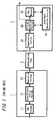
- FIG. 1 shows an example of configuration of a communication system which transmits and receives data at an arbitrary data rate among a plurality of predetermined data rates, and which includes a conventional reception device 3.
- the transmission device 1 transmits convolutionally coded data at an arbitrary data rate among a plurality of predetermined data rates to the reception device 3, via the communication path 2.
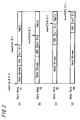
- FIG. 2 shows an example of the transport format of data here being transmitted and received.
- a CRC Cyclic Redundancy Check
- the tail bit final bit of the CRC
- the final bit of the CRC shall be called the tail bit n end .
- the tail bits n end for each of the data rates R1 to R4 become the E1st bit ((a) in FIG. 2), the E2nd bit ((b) in FIG. 2), the E3rd bit ((c) in FIG. 2), or the E4th bit ((d) in FIG. 2), counting from the leading bit S.
- the reception device 3 performs Viterbi decoding of data (FIG. 2) transmitted from the transmission device 1 via the communication path 2.
- the reception device 3 also detects the data rate of the received data, and outputs decoded data, at the detected data rate, to a data processing device (not shown) connected to the reception device.
- the transmission device 1 has a CRC (Cyclic Redundancy Check) encoder 11, convolutional coding portion 12, and modulation portion 13.
- the CRC encoder 11 appends to the data stream a CRC parity bit for data to be transmitted, and supplies the result to the convolutional coding portion 12.
- the convolutional coding portion 12 performs convolutional coding of the data from the CRC encoder 11, and supplies the result to the modulation portion 13.
- the modulation portion 13 modulates the data from the convolutional coding portion 12, and transmits the result to the reception device 3 via the communication path 2.
- the reception device 3 has a demodulation portion 31, Viterbi decoding portion 32, CRC decoder 33, and data rate detection portion 34.
- the demodulation portion 31 demodulates the received data, and supplies the result to the Viterbi decoding portion 32.
- the Viterbi decoding portion 32 is controlled by the data rate detection portion 34, and performs Viterbi decoding of data from the demodulation portion 31, supplying the data thus obtained (decoded data) to the CRC decoder 33.
- the Viterbi decoding portion 32 supplies to the data rate detection portion 34 the maximum path metric, minimum path metric, and zero-state path metric calculated at this time.
- the Viterbi decoding portion 32 outputs the decoded data obtained as a result of Viterbi decoding to a device, not shown, at the data rate detected by the data rate detection portion 34.
- the CRC decoding portion 33 is controlled by the data rate detection portion 34, and performs a CRC check of the data from the Viterbi decoding portion 32, supplying the check result to the data rate detection portion 34.
- the data rate detection portion 34 controls the Viterbi decoding portion 32 and CRC decoder 33, causing Viterbi decoding and CRC checks to be performed, and also detects the data rate of the received data based on the maximum path metric, minimum path metric and zero-state path metric, as well as the CRC check result from the CRC decoder 33.
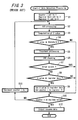
- step S1 the data rate detection portion 34 sets the initial values of the internal counter i to 1, of the register Smin to a predetermined value D, and of the register Tr to 0.
- step S2 the data rate detection portion 34 controls the Viterbi decoding portion 32 to compute the maximum path matrix, minimum path metric, and zero-state path metric from the leading bit S up to the tail bit n end for the data rate Ri identified using the value of the counter i.
- the Viterbi decoding portion 32 executes so-called ACS (Add-Compare-Select) processing to add, compare, and select values, and computes values of the maximum path metric, minimum path metric, and zero-state path metric.
- ACS Additional Compare-Select
- the Viterbi decoding portion 32 supplies the computed data to the data rate detection portion 34.
- the reception device 3 (data rate detection portion 34) identifies in advance the possible data rates Ri, and can identify the data rate Ri based on the value of the counter i.
- the data rates R1, R2, R3, R4 are respectively identified, and the maximum path metric, minimum path metric, and zero-state path metric from the leading bit S to the E1st bit ((a) in FIG. 2), E2nd bit ((b) in FIG. 2), E3rd bit ((c) in FIG. 2), or E4th bit ((d) in FIG. 2) are computed.
- step S3 the data rate detection portion 34 employs equation (1) to compute the S value based on the values for the maximum path metric, minimum path metric, and zero-state path metric supplied by the Viterbi decoding portion 32 in step S2.
- S value 10Log((a 0 -a min )/(a max -a min ))
- a max is the maximum path metric
- a min is the minimum path metric
- a 0 is the zero-state path metric.
- the maximum value of S is 0, and the minimum value is negative infinity.
- step S4 the data rate detection portion 34 judges whether the value of S computed in step S3 is or is not less than or equal to the threshold D.
- the zero-state path metric calculated by the Viterbi decoding portion 32 is a sufficiently small value, so that the value of S indicated by equation (1) is a small value. If on the other hand the data rate Ri is not the true data rate of the received data, the zero-state path metric calculated will not be a value that is sufficiently small, so that the value of S will not be a small value. In other words, by judging whether or not the calculated value of S is less than or equal to the threshold D, it is possible to decide whether the data rate Ri identified using the value of the counter i can be regarded as the true data rate of the received data (whether it is possible that the data rate is the true data rate).
- the threshold D is a comparatively large value, so that the S value for the true data rate is not judged to be larger than the threshold D.
- step S4 when the S value is judged to be equal to or less than the threshold D, that is, when the data rate Ri identified from the value of the counter i can be considered to be the true data rate for the received data (when there is the possibility that the data rate is the true data rate) , processing proceeds to step S5.
- step S5 the data rate detection portion 34 controls the Viterbi decoding portion 32 to cause execution of traceback processing, and generates the data stream up to the tail bit n end for the data rate Ri identified by the value of the counter i (for example, if the value of the counter i is 1, the E1st bit). Further, in step S6, the data rate detection portion 34 controls the CRC decoder 33 to cause a CRC check of the data thus generated to be performed.
- the Viterbi decoding portion 32 generates the data stream from the leading bit S to the tail bit n end for the data rate Ri, and supplies the data stream to the CRC decoder 33.
- the CRC decoder 33 divides the decoded data supplied by the Viterbi decoding portion 32 (the decoded data from the leading data bit S to the tail bit n end for the data rate Ri) by a generator polynomial, and determines the remainder.
- the CRC decoder 33 notifies the data rate detection portion 34 of the remainder thus determined, as the CRC calculation result.
- step S7 the data rate detection portion 34 judges whether or not an error exists in the received data, based on the CRC calculation result from the CRC decoder 33. That is, a judgment is made as to whether there exists an error in the received data, based on CRC calculation results for the case in which the data rate of the received data is the data rate Ri indicated by the value of the counter i at that time. If the CRC calculation result is not 0 (if the data rate Ri is not the true data rate), it is judged that an error exists, and if the CRC calculation result is 0 (if there is the possibility that the data rate is the true data rate), it is judged that an error does not exist.
- step S7 When in step S7 it is judged that an error does not exist, processing proceeds to step S8, and the data rate detection portion 34 judges whether or not the value S calculated in step S3 is equal to or less than the value of the register Smin.
- the value D is initially set as the register Smin, so that an S value initially resulting in a "YES" judgment in step S4 will of course be equal to or less than the value of the register Smin.
- step S8 when the value of S is judged to be equal to or less than the value of the register Smin, processing proceeds to step S9, and the data rate detection portion 34 replaces the value of the register Smin with the currently calculated value of S.
- the judgment of step S8 is a judgment of whether the currently calculated value of S is the smallest among the values of S calculated thus far.
- the data rate detection portion 34 also replaces the value of the register Tr with the current value of the counter i.
- step S4 When in step S4 it is judged that the value of S is not less than or equal to the threshold D, or when in step S7 an error is judged to exist, or when in step S8 the value of S is judged not to be less than or equal to the value of the register Smin, or when in step S9 the values of the register Smin and of the register Tr are interchanged, processing proceeds to step S10.
- step S10 the data rate detection portion 34 judges whether the value of the counter i is the maximum value (4), and if judged not to be the maximum value, processing proceeds to step S11, the value of the counter i is incremented by 1, processing returns to step S2, and subsequent processing is executed.
- step S10 When in step S10 the value of the counter i is judged to be the maximum value, processing proceeds to step S12, and the data rate detection portion 34 detects the data rate Ri identified by the value of the register Tr as the true data rate of the received data.
- the data rate detection portion 34 controls the Viterbi decoding portion 32 to cause decoded data to be output at the detected data rate Ri. Then, processing ends.
- This invention was devised in light of the above problem, and has as an object of performing detection of the rate of received data through simple processing.
- the signal processing device of this invention includes: normalization means for calculating the average value of received data and for utilizing the average value thus calculated to normalize the received data; maximum likelihood decoding means for selecting a plurality of data items in a predetermined order from among the output of the normalization means and performing maximum likelihood decoding processing, considering the rate of the data to be the selected data rate; computation means for subtracting the smallest metric value from among predetermined metric values obtained in the maximum likelihood decoding processing; judgment means for judging the correct data rate, based on metric values at state 0 for each rate obtained as a result of computations by the computation means and on error detection results; and output means for output of decoded data at the rate judged by the judgment means.
- the signal processing method of this invention includes the steps of: calculating the average value of received data and utilizing the average value thus calculated to normalize the received data; selecting a plurality of data items in a predetermined order from among the output of the normalization step and performing maximum likelihood decoding processing, considering the rate of the data to be the selected data rate; subtracting the smallest metric value from among predetermined metric values obtained in the step of maximum likelihood decoding processing; judging the correct data rate, based on metric values at state 0 for each rate obtained as a result of subtracting step and on error detection results; and outputting decoded data at the rate judged by the judging step.
- FIGS. 4 through 10 an embodiment of the present invention is explained.
- components corresponding to those in FIGS. 1 through 3 explaining an example of the prior art are assigned the same symbols.
- the invention is applied to a communication system in which convolutionally coded data is transmitted and received at an arbitrary data rate among a plurality of predetermined data rates. That is, in this embodiment a data format is used in which there exist four data rates, R1, R2, R3 and R4 (where data rate R1 ⁇ data rate R2 ⁇ data rate R3 ⁇ data rate R4), for which the respective positions of the tail bit n end are the E1st bit ((a) in FIG. 2), the E2nd bit ((b) in FIG. 2), the E3rd bit ((c) in FIG. 2), or the E4th bit ((d) in FIG. 2), counting from the leading bit S, as shown in FIG. 2.
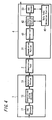
- FIG. 4 is a block diagram showing an example of the configuration of a communication system, including the reception device 4 of this embodiment.
- the configuration on the side of the transmission device 1 is the same as the configuration explained in the example of the prior art. That is, the transmission device 1 transmits convolutionally coded data to the reception device 4 via the communication path 2, at an arbitrary data rate among a plurality of predetermined data rates.
- the transmission device 1 has a CRC (Cyclic Redundancy Check) encoder 11, a convolutional coding portion 12, and a modulation portion 13.
- the CRC encoder 11 appends to the data stream a CRC parity bit for the data to be transmitted, and supplies the result to the convolutional coding portion 12.
- the convolutional coding portion 12 performs convolutional coding of the data from the CRC encoder 11, and supplies the result to the modulation portion 13.
- the modulation portion 13 modulates the data from the convolutional coding portion 12, and transmits the result to the reception device 4, via the communication path 2.
- the reception device 4 performs Viterbi decoding processing of data transmitted from the transmission device 1 via the communication path 2.
- the reception device 4 also detects the data rate of the received data, and outputs the decoded data to a data processing device (not shown) connected to the reception device at the detected data rate.
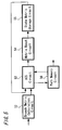
- the reception device 4 is configured including: a demodulation portion 31; normalizer 41 to normalize signals demodulated by the demodulation portion 31; Viterbi decoding portion 42 to perform Viterbi decoding of the output of the normalizer 41; CRC decoder 33 to perform CRC decoding of data output by the Viterbi decoding portion 42; and data rate detection portion 43 to detect the data rate of the received data.
- the demodulation portion 31 demodulates received data and supplies the result to the normalizer 41.
- the average value of the received data is calculated, and this calculated average value is used to normalize the received data. Specifically, the average value of the absolute values of data from, for example, the leading bit S until the tail bit n end that is the shortest data length at the data rate is calculated.
- Each of the input data items is divided by the calculated average values, and the result is further multiplied by an appropriate constant A.
- Demodulated data which has been normalized by the normalizer 41 is then Viterbi-decoded by the Viterbi decoding portion 42.
- FIG. 5 shows an example of the configuration of the Viterbi decoding portion 42.
- Data input to the Viterbi decoding portion 42 is supplied to a branch metric calculation circuit 52, and the metric for each branch is calculated by the branch metric calculation circuit 52.
- the branch metrics output by the branch metric calculation circuit 52, and the path metrics for each state stored in a state metric storage circuit 55, are supplied to an ACS circuit 53, added and compared.
- the path metrics for each state obtained by addition and comparison in the ACS circuit 53 are used by a metric reset circuit 54 to search for the minimum path metric, and the minimum path metric thus found is used to be subtracted from path metrics for each state in normalization computation processing, to reset the path metric for each state. By performing such reset processing, the minimum path metric is always 0.
- the path metrics for each state output by the reset circuit 54 are stored in the metric storage circuit 55 and are supplied to the ACS circuit 53.
- Path selection information in the ACS circuit 53 is stored in a path memory circuit 56.
- branch metrics and path metrics are added and compared for each of two paths merging in each state, based on the branch metrics supplied by the branch metric calculation circuit 52 and on the path metrics for each state stored in the metric storage circuit 55; based on the comparison results, metrics with the highest likelihood are selected, and are taken to be the new path metrics for each state.
- the details of the selection are supplied as path selection information to the path memory circuit 56, and the state number of the minimum metric is supplied as maximum-likelihood state information to the path memory circuit 56.
- the path memory circuit 56 stores path selection information output by the ACS circuit 53, and at the same time based on the maximum-likelihood state information output by the ACS circuit 53, outputs as decoded data the information, among the information corresponding to the maximum-likelihood path, until a specific length called the truncation length.
- An example of a specific path selection processing state is shown in the trellis of FIG. 6; if for example there exist four states S0, S1, S2, S3, there exist, for each time slot, two merging paths for all states. For each of the two paths merging into a given state, the Hamming distance (branch metric) between the received signal and the path, and the cumulative sum of branch metrics up to that time (state path metrics), are added and compared by the ACS circuit 53, and based on the comparison result, the path of highest likelihood is selected.
- the metric values of each of the states S0 to S3 are added cumulatively as shown in FIG. 6, and gradually a large value is obtained; by traversing the path with the smallest value in order, the path of maximum likelihood can be selected, and accurate decoding can be performed.
- FIG. 6 is a trellis illustrating the principle of path selection; as the metric for each state, the state is shown in which processing to subtract the minimum value is not performed at that time.
- metrics are shown in a state of cumulative addition, however as already explained, by performing the computation processing of this embodiment, the smallest value among the four states is 0.
- the smallest path metric is sought from the path metrics for each state obtained after the ACS (Add-Compare-Select) computations which add, compare, and select upon decoding at every step, and this minimum value is subtracted from the path metrics for each state.
- ACS Additional Compare-Select
- the reception device 4 of this embodiment only the zero-state path metric a 0' is supplied to the data rate detection portion 43.
- the Viterbi decoding portion 42 and CRC decoder 33 are controlled to and made to perform Viterbi decoding and CRC checking, and based on the zero-state path metric a 0 , from the Viterbi decoding portion 42 and the result of CRC checking by the CRC decoder 33, processing is performed to detect the data rate of the received data.
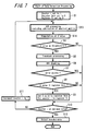
- step S1 the data rate detection portion 43 sets the initial values of the counter i to 1, of the value of the register Smin to the predetermined value D, and of the value of the register Tr to 0.
- the Viterbi decoding portion 42 executes in sequence the ACS processing already described, involving addition, comparison and selection of data normalized by the normalizer 41, and seeks the smallest path metric among the path metric values for each state obtained after ACS processing; this value is subtracted from the path metric values for each state. Further, the Viterbi decoding portion 42 is controlled by the data rate detection portion 43, and supplies to the data rate detection portion 43 the zero-state path metric a 0 , at the tail bit n end for the data rate Ri identified by the value of the counter i.
- the data rate detection portion 43 within the reception device 4 identifies in advance all possible data rates Ri, and is able to recognize the data rate Ri based on the value of the counter i.
- the data rates R1, R2, R3, R4 respectively are recognized, and the values of the maximum path metric, minimum path metric, and zero-state path metric are calculated for data from the leading bit S until the E1st bit ((a) in FIG. 2), the E2nd bit ( (b) in FIG. 2), the E3rd bit ((c) in FIG. 2), or the E4th bit ((d) in FIG. 2), respectively.
- step S14 the data rate detection portion 43 computes the following equation to calculate the S value, based on the zero-state path metric a 0' supplied by the Viterbi decoding portion 42 in step S13.
- S value a 0'
- the S value is the value of a 0' itself supplied by the Viterbi decoding portion 42. Using this S value, the subsequent processing is performed. The subsequent processing steps are the same as the processing steps explained in the example of the prior art; however, the explanation is here repeated.
- the data rate detection portion 43 judges whether or not the S value computed in step S14 is equal to or less than the threshold D.
- the zero-state path metric calculated by the Viterbi decoding portion 42 at this time will be sufficiently small, and so the S value indicated by equation (2) will be a small value.
- the zero-state path metric calculated at this time will not be a small value, and so the S value will not be a small value. That is, by judging whether or not the computed S value is equal to or less than the threshold D, it is possible to judge whether or not the data rate Ri identified by the value of the counter i is the true data rate of the received data (whether it is possible that the data rate is the true data rate).
- the threshold D is set to a comparatively large value, such that the S value for the true data rate is not judged to be larger than the threshold D.
- step S4 when the S value is judged to be equal to or less than the threshold D, that is, when the data rate Ri identified by the value of the counter i at this time can be regarded as the true data rate of the received data (when there is the possibility that the data rate is the true data rate), processing proceeds to step S5.
- step S5 the data rate detection portion 43 controls the Viterbi decoding portion 42 to cause traceback processing to be executed, to generate the data stream from the leading bit S until the tail bit n end for the data rate Ri identified by the value of the counter i (for example, when the value of the counter i is 1, the E1st bit). Then, in step S6, the data rate detection portion 43 controls the CRC decoder 33 to cause a CRC check of the data generated to be performed.
- the Viterbi decoding portion 42 generates the data stream from the leading bit S until the tail bit n end for the data rate Ri, and supplies the result to the CRC decoder 33.
- the CRC decoder 33 divides the decoded data supplied by the Viterbi decoding portion 42 (the decoded data from the leading data bit S to the tail bit n end for the data rate Ri) by a generator polynomial, and determines the remainder.
- the CRC decoder 33 notifies the data rate detection portion 43 of the calculated remainder, as the CRC calculation result.
- step S7 the data rate detection portion 43 judges whether or not there exists an error in the received data, based on the CRC calculation result from the CRC decoder 33. That is, a judgment is made as to whether there exists an error in the received data based on the CRC calculation results for the case in which the data rate of the received data is the data rate Ri indicated by the value of the counter i at this time. If the CRC calculation result is not 0 (if the data rate Ri is not the true data rate), it is judged that an error exists; if the CRC calculation result is 0 (when there is a possibility that the data rate is the true data rate), it is judged that an error does not exist.
- step S7 when it is judged that an error has not occurred, processing proceeds to step S8, and the data rate detection portion 43 judges whether or not the S value computed in step S14 is equal to or less than the value of register Smin.
- the value D is initially set as the register Smin, and so an S value which initially results in a "YES" judgment in step S4 is of course equal to or less than the value of the register Smin.
- step S8 when the S value has been judged to be equal to or less than the value of the register Smin, processing proceeds to step S9, and the data rate detection portion 43 replaces the value of the register Smin with the S value just calculated. That is, the judgment in step S8 is a judgment as to whether the S value just calculated is the smallest among the S values calculated thus far.
- the data rate detection portion 43 also replaces the value of the register Tr with the value of the counter i at this time.
- step S4 When in step S4 the S value is judged to be equal to or less than the threshold D, when in step S7 it is judged that an error exists, when in step S8 it is judged that the S value is judged not to be equal to or less than the value of the register Smin, or when in step S9 the values of the register Smin and of the register Tr are replaced, processing proceeds to step S10.
- step S10 the data rate detection portion 43 judges whether or not the value of the counter i is the maximum value (4) or not; when judged not to be the maximum value, processing proceeds to step S11, the value of the counter i is incremented by 1, processing returns to step S13, and subsequent processing is executed.
- step S10 When in step S10 the value of the counter i is judged to be the maximum value, processing proceeds to step S12, and the data rate detection portion 43 detects the data rate Ri identified by the value of the register Tr as the true data rate of the received data. The data rate detection portion 43 then controls the Viterbi decoding portion 42 to cause the decoded data at the detected data rate Ri to be output. Then processing ends.
- the S value necessary for data rate detection of received data can be obtained through simple processing. That is, in the prior art it was necessary to perform the complicated computations indicated by equation (1) to obtain the S value; however, in this embodiment, through normalization processing by the normalizer 41 and subtraction of the smallest path metric by the Viterbi decoding portion 42, the S value can be obtained as the zero-state path metric after subtraction of the smallest metric supplied by the Viterbi decoding portion 42, so that the amount of calculation for data rate detection can be reduced.
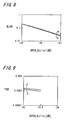
- FIG. 8 plots the block error rate (BLER) along the vertical axis and the transmission power from a base station along the horizontal axis, as an example measured in a 240 Hz fading state.
- the block error rate is the probability of failure of data rate detection processing with the register Tr left at the initial value of 0.
- the characteristic a is the S value error rate computed using the processing of this embodiment (equation (2)); the characteristic b is the S value error rate computed using conventional processing (equation (1)). There is almost no difference between the two characteristics.
- FIG. 9 plots the FDR (Fault Detection Rate) along the vertical axis and the transmission power from the base station along the horizontal axis, as an example measured in a 240 Hz fading state.
- the FDR is the probability that the transmission data rate and the detected data rate are different.
- the characteristic c is the S value error rate computed using the processing of this embodiment (equation (2)); the characteristic d is the S value error rate computed using conventional processing (equation (1)). In this case also, there is almost no difference between the characteristics.
- the dynamic range can be reduced in the later-stage Viterbi decoding portion. Without a normalizer, it would be necessary to secure a broad dynamic range accommodating all possible input ranges. By further performing quantization and limiting in the course of this processing, the data bit width can also be reduced, and so the circuit scale of the Viterbi decoding portion 42 can be further decreased.
- the series of processing explained thus far can be implemented in hardware, but can also be realized in software.
- a program comprising the software is installed in a computer or other data processing equipment, and by executing the program on the computer or similar, the above-described reception device 4 is functionally realized.
- FIG. 10 is a block diagram showing an example of the configuration of a computer 101 functioning as a reception device 4 similar to that described above.
- An input/output interface 116 is connected via a bus 115 to a CPU (Central Processing Unit) 111, and upon input of an instruction by the user from the input portion 118 via the input/output interface 116 using a keyboard, mouse or similar, the CPU 111 loads into RAM (Random Access Memory) 113 and executes a program stored in, for example, ROM (Read-Only Memory) 112, a hard disk 114, or a magnetic disc 131, optical disc 132, or magneto-optical disc 133 loaded into a drive 120, or in semiconductor memory 134 or other recording media.
- ROM Read-Only Memory
- the various processing described above (for example, the processing indicated in the flowchart of FIG. 7) is performed. Further, the CPU 111 outputs processing results via, for example, the input/output interface 116, to a LCD (Liquid Crystal Display) or other display portion 117 as necessary.
- the program can be stored in advance on the hard disk 114 or in ROM 112 and supplied integrally with the computer 101 to a user; or can be supplied in packaged media such as a magnetic disk 131, optical disc 132, magneto-optical disc 133, semiconductor memory 134 or similar; or can be supplied to the hard disk 114 from a satellite, network or similar via the communication portion 119.
- the steps describing a program to be supplied using recording media include, in addition to processing performed in time series following the order described, processing not necessarily in time series, and also processing executed in parallel or individually.
Landscapes
- Engineering & Computer Science (AREA)
- Computer Networks & Wireless Communication (AREA)
- Signal Processing (AREA)
- Artificial Intelligence (AREA)
- Error Detection And Correction (AREA)
- Detection And Prevention Of Errors In Transmission (AREA)
- Detection And Correction Of Errors (AREA)
Applications Claiming Priority (2)
| Application Number | Priority Date | Filing Date | Title |
|---|---|---|---|
| JP2002367195A JP3852401B2 (ja) | 2002-12-18 | 2002-12-18 | 信号処理装置及び方法 |
| JP2002367195 | 2002-12-18 |
Publications (2)
| Publication Number | Publication Date |
|---|---|
| EP1432165A1 true EP1432165A1 (fr) | 2004-06-23 |
| EP1432165B1 EP1432165B1 (fr) | 2006-08-30 |
Family
ID=32376278
Family Applications (1)
| Application Number | Title | Priority Date | Filing Date |
|---|---|---|---|
| EP03028693A Expired - Lifetime EP1432165B1 (fr) | 2002-12-18 | 2003-12-16 | Procédé et dispositif pour le décodage de données à débit variable |
Country Status (5)
| Country | Link |
|---|---|
| US (1) | US7228491B2 (fr) |
| EP (1) | EP1432165B1 (fr) |
| JP (1) | JP3852401B2 (fr) |
| KR (1) | KR20040054539A (fr) |
| DE (1) | DE60307968T2 (fr) |
Cited By (4)
| Publication number | Priority date | Publication date | Assignee | Title |
|---|---|---|---|---|
| WO2006106377A1 (fr) * | 2005-04-07 | 2006-10-12 | Nokia Corporation | Detection en aveugle du format de transport sur la base d'une metrique de decodeur |
| WO2007139566A1 (fr) * | 2006-05-31 | 2007-12-06 | Agere Systems Inc. | Procédé et appareil destinés à une détection en aveugle du format de transport utilisant une détection de transmission discontinue (dtx) |
| KR100939422B1 (ko) * | 2005-04-07 | 2010-01-28 | 노키아 코포레이션 | 디코더 메트릭에 의거한 블라인드 전송 포맷 검출 |
| WO2016018857A1 (fr) * | 2014-07-28 | 2016-02-04 | Qualcomm Incorporated | Réduction de fausse détection par contrôle de redondance cyclique (crc) dans des systèmes de communication |
Families Citing this family (8)
| Publication number | Priority date | Publication date | Assignee | Title |
|---|---|---|---|---|
| US7463702B2 (en) * | 2002-11-12 | 2008-12-09 | Agere Systems Inc. | System and method for one-pass blind transport format detection |
| EP1575176A1 (fr) * | 2004-03-09 | 2005-09-14 | Deutsche Thomson-Brandt Gmbh | Dispositif pour récupérer une séquence binaire par une méthode adaptative |
| CA3023907C (fr) | 2004-09-25 | 2019-06-04 | Tq Delta, Llc | Normalisation de compteur crc |
| KR101240503B1 (ko) * | 2006-02-24 | 2013-03-08 | 삼성전자주식회사 | 비동기식 이동통신 시스템에서 방송 채널의 동기 검출 방법및 장치 |
| JP4806673B2 (ja) * | 2007-12-27 | 2011-11-02 | ルネサスエレクトロニクス株式会社 | 復号装置及び復号方法 |
| TWI450266B (zh) * | 2011-04-19 | 2014-08-21 | Hon Hai Prec Ind Co Ltd | 電子裝置及音頻資料的解碼方法 |
| EP2696527B1 (fr) * | 2012-08-09 | 2016-07-27 | ST-Ericsson SA | Détection aveugle de format de transport améliorée en fonction des conditions de réception du signal |
| US10880062B2 (en) * | 2017-06-29 | 2020-12-29 | Qualcomm Incorporated | Providing protection for information delivered in demodulation reference signals (DMRS) |
Citations (3)
| Publication number | Priority date | Publication date | Assignee | Title |
|---|---|---|---|---|
| EP0763902A1 (fr) * | 1995-09-15 | 1997-03-19 | Nokia Mobile Phones Ltd. | Procédé et appareil de détermination de la vitesse de transmission basée sur la croissance d'une métrique de chemin dans un decodeur Viterbi |
| EP1187343A2 (fr) * | 2000-08-31 | 2002-03-13 | Sony Corporation | Appareil et méthode de démodulation de données |
| EP1207659A2 (fr) * | 2000-11-17 | 2002-05-22 | NTT DoCoMo, Inc. | Méthode de transmission de données, système de transmission de données, émetteur et recépteur |
Family Cites Families (4)
| Publication number | Priority date | Publication date | Assignee | Title |
|---|---|---|---|---|
| JP2596392B2 (ja) | 1994-11-16 | 1997-04-02 | 日本電気株式会社 | データレート検出器 |
| JP3251591B2 (ja) | 1995-07-25 | 2002-01-28 | モトローラ・インコーポレイテッド | オン/オフ可変レート通信システムにおけるレート判定の装置および方法 |
| JP2002076923A (ja) | 2000-08-30 | 2002-03-15 | Sony Corp | 信号処理装置および方法、並びに記録媒体 |
| US6795511B1 (en) * | 2000-09-27 | 2004-09-21 | Storage Technology Corporation | Method for reducing the sensitivity of a maximum likelihood detection trellis to channel variations |
-
2002
- 2002-12-18 JP JP2002367195A patent/JP3852401B2/ja not_active Expired - Fee Related
-
2003
- 2003-12-16 EP EP03028693A patent/EP1432165B1/fr not_active Expired - Lifetime
- 2003-12-16 DE DE60307968T patent/DE60307968T2/de not_active Expired - Fee Related
- 2003-12-17 KR KR1020030092467A patent/KR20040054539A/ko not_active Withdrawn
- 2003-12-17 US US10/739,985 patent/US7228491B2/en not_active Expired - Fee Related
Patent Citations (3)
| Publication number | Priority date | Publication date | Assignee | Title |
|---|---|---|---|---|
| EP0763902A1 (fr) * | 1995-09-15 | 1997-03-19 | Nokia Mobile Phones Ltd. | Procédé et appareil de détermination de la vitesse de transmission basée sur la croissance d'une métrique de chemin dans un decodeur Viterbi |
| EP1187343A2 (fr) * | 2000-08-31 | 2002-03-13 | Sony Corporation | Appareil et méthode de démodulation de données |
| EP1207659A2 (fr) * | 2000-11-17 | 2002-05-22 | NTT DoCoMo, Inc. | Méthode de transmission de données, système de transmission de données, émetteur et recépteur |
Cited By (13)
| Publication number | Priority date | Publication date | Assignee | Title |
|---|---|---|---|---|
| CN101151836B (zh) * | 2005-04-07 | 2014-06-04 | 诺基亚公司 | 检测数据网络中数据块的块长度的方法、装置和系统 |
| KR100939422B1 (ko) * | 2005-04-07 | 2010-01-28 | 노키아 코포레이션 | 디코더 메트릭에 의거한 블라인드 전송 포맷 검출 |
| US8286058B2 (en) | 2005-04-07 | 2012-10-09 | Nokia Corporation | Blind transport format detection based on decoder metric |
| WO2006106377A1 (fr) * | 2005-04-07 | 2006-10-12 | Nokia Corporation | Detection en aveugle du format de transport sur la base d'une metrique de decodeur |
| WO2007139566A1 (fr) * | 2006-05-31 | 2007-12-06 | Agere Systems Inc. | Procédé et appareil destinés à une détection en aveugle du format de transport utilisant une détection de transmission discontinue (dtx) |
| GB2452216A (en) * | 2006-05-31 | 2009-02-25 | Agere Systems Inc | Method and apparatus for blind transport format detection using discontinuous transmission (DTX) detection |
| GB2452216B (en) * | 2006-05-31 | 2011-05-25 | Agere Systems Inc | Method and apparatus for blind transport format detection using discontinuous transmission (DTX) detection |
| US8121104B2 (en) | 2006-05-31 | 2012-02-21 | Agere Systems Inc. | Method and apparatus for blind transport format detection using discontinuous transmission (DTX) detection |
| KR101133844B1 (ko) | 2006-05-31 | 2012-04-06 | 에이저 시스템즈 인크 | 트랜스포트 포맷 결정 방법 및 시스템 |
| US8351412B2 (en) | 2006-05-31 | 2013-01-08 | Agere Systems Llc | Method and apparatus for blind transport format detection using discontinuous transmission (DTX) detection |
| WO2016018857A1 (fr) * | 2014-07-28 | 2016-02-04 | Qualcomm Incorporated | Réduction de fausse détection par contrôle de redondance cyclique (crc) dans des systèmes de communication |
| US9558062B2 (en) | 2014-07-28 | 2017-01-31 | Qualcomm Incorporated | Cyclic redundancy check (CRC) false detection reduction in communication systems |
| CN106576018A (zh) * | 2014-07-28 | 2017-04-19 | 高通股份有限公司 | 通信系统中的循环冗余校验(crc)误检减少 |
Also Published As
| Publication number | Publication date |
|---|---|
| KR20040054539A (ko) | 2004-06-25 |
| JP3852401B2 (ja) | 2006-11-29 |
| DE60307968T2 (de) | 2007-03-01 |
| EP1432165B1 (fr) | 2006-08-30 |
| DE60307968D1 (de) | 2006-10-12 |
| US7228491B2 (en) | 2007-06-05 |
| US20040133842A1 (en) | 2004-07-08 |
| JP2004201030A (ja) | 2004-07-15 |
Similar Documents
| Publication | Publication Date | Title |
|---|---|---|
| RU2414077C2 (ru) | Схема формирования сигнала коммутации каналов и способ формирования сигнала коммутации каналов | |
| JP3120511B2 (ja) | ビタビ復号装置 | |
| US6065149A (en) | Error correction device for a communication system | |
| US8671335B2 (en) | Soft output Viterbi detector with error event output | |
| EP1069721B1 (fr) | Système et procédé pour fixer le débit de données dans un système de communication sans fil | |
| EP1432165B1 (fr) | Procédé et dispositif pour le décodage de données à débit variable | |
| JPH09181619A (ja) | ビタービ復号器とその復号方法 | |
| US7062687B1 (en) | Apparatus and method for setting a data rate in a wireless communication system | |
| US8230308B2 (en) | Decoding apparatus and decoding method using an additional add-compare-select operation on decoded data in the event of an error in the decoded data | |
| CN1167201C (zh) | 使用零状态度量值的维特比解码数据质量计算装置 | |
| JPH10133898A (ja) | 畳み込みエンコードデータのエラー検出およびエラー補正方法 | |
| US6058501A (en) | Error detecting device for viterbi decoder | |
| US6483881B1 (en) | Method of reducing complexity using statistics of path metrics in a trellis decoder | |
| US6915474B2 (en) | Turbo decoding apparatus and decoding iteration count controlling method in turbo decoding | |
| US7184409B2 (en) | Blind rate detection method and device in asynchronous mobile communication system | |
| US20070153693A1 (en) | Transport format detecting apparatus and method | |
| KR20020018092A (ko) | 신호 처리 장치, 신호 처리 방법 및 기록 매체 | |
| EP1387516A1 (fr) | Détection aveugle de format de transport de données pour récepteurs à spectre étalé | |
| US20030229842A1 (en) | Method for calculating syndrome polynomial in decoding error correction codes | |
| JPH0349426A (ja) | ヴィタビ復号器 | |
| JP3847181B2 (ja) | 軟判定ビタビ復号装置 | |
| KR100459419B1 (ko) | 비터비 디코더 | |
| US20110090994A1 (en) | Decoding Method and Associated Apparatus | |
| JPH10145242A (ja) | ビタビ復号方法および装置 | |
| JPH0349427A (ja) | ヴィタビ復号器 |
Legal Events
| Date | Code | Title | Description |
|---|---|---|---|
| PUAI | Public reference made under article 153(3) epc to a published international application that has entered the european phase |
Free format text: ORIGINAL CODE: 0009012 |
|
| AK | Designated contracting states |
Kind code of ref document: A1 Designated state(s): AT BE BG CH CY CZ DE DK EE ES FI FR GB GR HU IE IT LI LU MC NL PT RO SE SI SK TR |
|
| AX | Request for extension of the european patent |
Extension state: AL LT LV MK |
|
| 17P | Request for examination filed |
Effective date: 20040623 |
|
| 17Q | First examination report despatched |
Effective date: 20050131 |
|
| AKX | Designation fees paid |
Designated state(s): DE GB |
|
| GRAP | Despatch of communication of intention to grant a patent |
Free format text: ORIGINAL CODE: EPIDOSNIGR1 |
|
| GRAS | Grant fee paid |
Free format text: ORIGINAL CODE: EPIDOSNIGR3 |
|
| GRAA | (expected) grant |
Free format text: ORIGINAL CODE: 0009210 |
|
| AK | Designated contracting states |
Kind code of ref document: B1 Designated state(s): DE GB |
|
| REG | Reference to a national code |
Ref country code: GB Ref legal event code: FG4D |
|
| REF | Corresponds to: |
Ref document number: 60307968 Country of ref document: DE Date of ref document: 20061012 Kind code of ref document: P |
|
| PGFP | Annual fee paid to national office [announced via postgrant information from national office to epo] |
Ref country code: DE Payment date: 20061214 Year of fee payment: 4 |
|
| PLBE | No opposition filed within time limit |
Free format text: ORIGINAL CODE: 0009261 |
|
| STAA | Information on the status of an ep patent application or granted ep patent |
Free format text: STATUS: NO OPPOSITION FILED WITHIN TIME LIMIT |
|
| 26N | No opposition filed |
Effective date: 20070531 |
|
| GBPC | Gb: european patent ceased through non-payment of renewal fee |
Effective date: 20071216 |
|
| PG25 | Lapsed in a contracting state [announced via postgrant information from national office to epo] |
Ref country code: DE Free format text: LAPSE BECAUSE OF NON-PAYMENT OF DUE FEES Effective date: 20080701 |
|
| PG25 | Lapsed in a contracting state [announced via postgrant information from national office to epo] |
Ref country code: GB Free format text: LAPSE BECAUSE OF NON-PAYMENT OF DUE FEES Effective date: 20071216 |