EP1439576A2 - Verfahren zur Herstellung eines Durchgangsloches - Google Patents
Verfahren zur Herstellung eines Durchgangsloches Download PDFInfo
- Publication number
- EP1439576A2 EP1439576A2 EP04250045A EP04250045A EP1439576A2 EP 1439576 A2 EP1439576 A2 EP 1439576A2 EP 04250045 A EP04250045 A EP 04250045A EP 04250045 A EP04250045 A EP 04250045A EP 1439576 A2 EP1439576 A2 EP 1439576A2
- Authority
- EP
- European Patent Office
- Prior art keywords
- metal film
- film
- semiconductor substrate
- forming
- bump metal
- Prior art date
- Legal status (The legal status is an assumption and is not a legal conclusion. Google has not performed a legal analysis and makes no representation as to the accuracy of the status listed.)
- Granted
Links
Images



Classifications
-
- H—ELECTRICITY
- H10—SEMICONDUCTOR DEVICES; ELECTRIC SOLID-STATE DEVICES NOT OTHERWISE PROVIDED FOR
- H10W—GENERIC PACKAGES, INTERCONNECTIONS, CONNECTORS OR OTHER CONSTRUCTIONAL DETAILS OF DEVICES COVERED BY CLASS H10
- H10W20/00—Interconnections in chips, wafers or substrates
- H10W20/01—Manufacture or treatment
- H10W20/021—Manufacture or treatment of interconnections within wafers or substrates
- H10W20/023—Manufacture or treatment of interconnections within wafers or substrates the interconnections being through-semiconductor vias
-
- H—ELECTRICITY
- H10—SEMICONDUCTOR DEVICES; ELECTRIC SOLID-STATE DEVICES NOT OTHERWISE PROVIDED FOR
- H10W—GENERIC PACKAGES, INTERCONNECTIONS, CONNECTORS OR OTHER CONSTRUCTIONAL DETAILS OF DEVICES COVERED BY CLASS H10
- H10W20/00—Interconnections in chips, wafers or substrates
- H10W20/01—Manufacture or treatment
- H10W20/021—Manufacture or treatment of interconnections within wafers or substrates
- H10W20/023—Manufacture or treatment of interconnections within wafers or substrates the interconnections being through-semiconductor vias
- H10W20/0238—Manufacture or treatment of interconnections within wafers or substrates the interconnections being through-semiconductor vias comprising etching via holes through pads or through electrodes
-
- H—ELECTRICITY
- H10—SEMICONDUCTOR DEVICES; ELECTRIC SOLID-STATE DEVICES NOT OTHERWISE PROVIDED FOR
- H10W—GENERIC PACKAGES, INTERCONNECTIONS, CONNECTORS OR OTHER CONSTRUCTIONAL DETAILS OF DEVICES COVERED BY CLASS H10
- H10W20/00—Interconnections in chips, wafers or substrates
- H10W20/01—Manufacture or treatment
- H10W20/021—Manufacture or treatment of interconnections within wafers or substrates
- H10W20/023—Manufacture or treatment of interconnections within wafers or substrates the interconnections being through-semiconductor vias
- H10W20/0245—Manufacture or treatment of interconnections within wafers or substrates the interconnections being through-semiconductor vias comprising use of blind vias during the manufacture
-
- H—ELECTRICITY
- H10—SEMICONDUCTOR DEVICES; ELECTRIC SOLID-STATE DEVICES NOT OTHERWISE PROVIDED FOR
- H10W—GENERIC PACKAGES, INTERCONNECTIONS, CONNECTORS OR OTHER CONSTRUCTIONAL DETAILS OF DEVICES COVERED BY CLASS H10
- H10W20/00—Interconnections in chips, wafers or substrates
- H10W20/20—Interconnections within wafers or substrates, e.g. through-silicon vias [TSV]
-
- H—ELECTRICITY
- H10—SEMICONDUCTOR DEVICES; ELECTRIC SOLID-STATE DEVICES NOT OTHERWISE PROVIDED FOR
- H10W—GENERIC PACKAGES, INTERCONNECTIONS, CONNECTORS OR OTHER CONSTRUCTIONAL DETAILS OF DEVICES COVERED BY CLASS H10
- H10W72/00—Interconnections or connectors in packages
- H10W72/01—Manufacture or treatment
- H10W72/012—Manufacture or treatment of bump connectors, dummy bumps or thermal bumps
-
- H—ELECTRICITY
- H10—SEMICONDUCTOR DEVICES; ELECTRIC SOLID-STATE DEVICES NOT OTHERWISE PROVIDED FOR
- H10W—GENERIC PACKAGES, INTERCONNECTIONS, CONNECTORS OR OTHER CONSTRUCTIONAL DETAILS OF DEVICES COVERED BY CLASS H10
- H10W90/00—Package configurations
-
- H—ELECTRICITY
- H10—SEMICONDUCTOR DEVICES; ELECTRIC SOLID-STATE DEVICES NOT OTHERWISE PROVIDED FOR
- H10W—GENERIC PACKAGES, INTERCONNECTIONS, CONNECTORS OR OTHER CONSTRUCTIONAL DETAILS OF DEVICES COVERED BY CLASS H10
- H10W72/00—Interconnections or connectors in packages
- H10W72/20—Bump connectors, e.g. solder bumps or copper pillars; Dummy bumps; Thermal bumps
- H10W72/251—Materials
-
- H—ELECTRICITY
- H10—SEMICONDUCTOR DEVICES; ELECTRIC SOLID-STATE DEVICES NOT OTHERWISE PROVIDED FOR
- H10W—GENERIC PACKAGES, INTERCONNECTIONS, CONNECTORS OR OTHER CONSTRUCTIONAL DETAILS OF DEVICES COVERED BY CLASS H10
- H10W72/00—Interconnections or connectors in packages
- H10W72/50—Bond wires
- H10W72/551—Materials of bond wires
- H10W72/552—Materials of bond wires comprising metals or metalloids, e.g. silver
- H10W72/5522—Materials of bond wires comprising metals or metalloids, e.g. silver comprising gold [Au]
-
- H—ELECTRICITY
- H10—SEMICONDUCTOR DEVICES; ELECTRIC SOLID-STATE DEVICES NOT OTHERWISE PROVIDED FOR
- H10W—GENERIC PACKAGES, INTERCONNECTIONS, CONNECTORS OR OTHER CONSTRUCTIONAL DETAILS OF DEVICES COVERED BY CLASS H10
- H10W72/00—Interconnections or connectors in packages
- H10W72/50—Bond wires
- H10W72/551—Materials of bond wires
- H10W72/552—Materials of bond wires comprising metals or metalloids, e.g. silver
- H10W72/5525—Materials of bond wires comprising metals or metalloids, e.g. silver comprising copper [Cu]
-
- H—ELECTRICITY
- H10—SEMICONDUCTOR DEVICES; ELECTRIC SOLID-STATE DEVICES NOT OTHERWISE PROVIDED FOR
- H10W—GENERIC PACKAGES, INTERCONNECTIONS, CONNECTORS OR OTHER CONSTRUCTIONAL DETAILS OF DEVICES COVERED BY CLASS H10
- H10W90/00—Package configurations
- H10W90/20—Configurations of stacked chips
- H10W90/297—Configurations of stacked chips characterised by the through-semiconductor vias [TSVs] in the stacked chips
-
- H—ELECTRICITY
- H10—SEMICONDUCTOR DEVICES; ELECTRIC SOLID-STATE DEVICES NOT OTHERWISE PROVIDED FOR
- H10W—GENERIC PACKAGES, INTERCONNECTIONS, CONNECTORS OR OTHER CONSTRUCTIONAL DETAILS OF DEVICES COVERED BY CLASS H10
- H10W90/00—Package configurations
- H10W90/701—Package configurations characterised by the relative positions of pads or connectors relative to package parts
- H10W90/721—Package configurations characterised by the relative positions of pads or connectors relative to package parts of bump connectors
- H10W90/722—Package configurations characterised by the relative positions of pads or connectors relative to package parts of bump connectors between stacked chips
-
- H—ELECTRICITY
- H10—SEMICONDUCTOR DEVICES; ELECTRIC SOLID-STATE DEVICES NOT OTHERWISE PROVIDED FOR
- H10W—GENERIC PACKAGES, INTERCONNECTIONS, CONNECTORS OR OTHER CONSTRUCTIONAL DETAILS OF DEVICES COVERED BY CLASS H10
- H10W90/00—Package configurations
- H10W90/701—Package configurations characterised by the relative positions of pads or connectors relative to package parts
- H10W90/721—Package configurations characterised by the relative positions of pads or connectors relative to package parts of bump connectors
- H10W90/724—Package configurations characterised by the relative positions of pads or connectors relative to package parts of bump connectors between a chip and a stacked insulating package substrate, interposer or RDL
-
- Y—GENERAL TAGGING OF NEW TECHNOLOGICAL DEVELOPMENTS; GENERAL TAGGING OF CROSS-SECTIONAL TECHNOLOGIES SPANNING OVER SEVERAL SECTIONS OF THE IPC; TECHNICAL SUBJECTS COVERED BY FORMER USPC CROSS-REFERENCE ART COLLECTIONS [XRACs] AND DIGESTS
- Y10—TECHNICAL SUBJECTS COVERED BY FORMER USPC
- Y10S—TECHNICAL SUBJECTS COVERED BY FORMER USPC CROSS-REFERENCE ART COLLECTIONS [XRACs] AND DIGESTS
- Y10S438/00—Semiconductor device manufacturing: process
- Y10S438/928—Front and rear surface processing
-
- Y—GENERAL TAGGING OF NEW TECHNOLOGICAL DEVELOPMENTS; GENERAL TAGGING OF CROSS-SECTIONAL TECHNOLOGIES SPANNING OVER SEVERAL SECTIONS OF THE IPC; TECHNICAL SUBJECTS COVERED BY FORMER USPC CROSS-REFERENCE ART COLLECTIONS [XRACs] AND DIGESTS
- Y10—TECHNICAL SUBJECTS COVERED BY FORMER USPC
- Y10S—TECHNICAL SUBJECTS COVERED BY FORMER USPC CROSS-REFERENCE ART COLLECTIONS [XRACs] AND DIGESTS
- Y10S438/00—Semiconductor device manufacturing: process
- Y10S438/977—Thinning or removal of substrate
Definitions
- the present invention relates to a semiconductor device manufacturing method and, more particularly, a method of manufacturing a semiconductor device having through wirings that make possible electrical conduction between connection terminals on an element forming surface side and connection terminals on a back surface side.
- a packaging structure in which a plurality of semiconductor chips are laminated and packaged three- dimensionally on the wiring substrate has been developed.
- As a method of implementing such a packaging structure there is the method of connecting the connection terminals on the element forming surface side of the semiconductor chip and the connection terminals on the back surface side via the through holes that pass through the semiconductor chip and then laminating plural times this semiconductor chip on a wiring substrate to be connected mutually.
- FIG.1A of the accompanying drawings first a semiconductor wafer 100 on which predetermined transistors, multi-layered wirings (not shown), etc. are formed and which has a thickness of about 400 ⁇ m is prepared. Connecting pads 102 are exposed from an upper surface of the semiconductor wafer 100, and portions except the connecting pads 102 are covered with a passivation film 104.
- a resist film (not shown) having opening portions at center portions of the connecting pads 102 is patterned on the connecting pads 102 and the passivation film 104 (masking step 1).
- the connecting pads 102 and the underlying semiconductor wafer 100 are etched sequentially by RIE (Reactive Ion Etching), or the like while using the resist film as a mask.
- RIE Reactive Ion Etching
- an insulating film 106 such as a silicon oxide film, or the like is formed on inner surfaces of the through holes 100a, the connecting pads 102, and the passivation film 104 by CVD, or the like.
- This insulating film 106 is formed to isolate electrically a conductive film, which is filled in the through holes 100a later, from the semiconductor wafer 100.
- a seed Cu film 110 is formed on the resultant structure in FIG.1D by electroless plating, sputter method, or the like. Then, a resist film 112 having opening portions 112a on the through holes 100a and the connecting pads 102 is formed (masking step 3).
- a Cu film pattern 114 is formed in interiors of the through holes 100a and the opening portions 112a of the resist film 112 by electroplating utilizing the seed Cu film 110 as a plating power-supply layer. Then, as shown in FIG.1F of the accompanying drawings, the resist film 112 is removed, and then the seed Cu film 110 is etched by using the Cu film pattern 114 as a mask. Thus, Cu bumps 114a each connected electrically to the connecting pad 102 and Cu plugs 114b each connected to this Cu bump 114a are formed.
- a thickness of the semiconductor wafer 100 is reduced by grinding the back surface of the semiconductor wafer 100 by virtue of a grinder.
- the semiconductor wafer 100 and the Cu plugs 114b filled in the through holes 100a are ground at the same time.
- top end portions of the Cu plugs 114b on the back surface side of the semiconductor wafer 100 act as connection terminals 114c on the back surface side.
- the connecting pads 102 and the Cu bumps 114a connected thereto on the element forming surface side of the semiconductor wafer 100 are connected to the connection terminals 114c on the back surface side via the through holes 100a.
- Patent Literature 1 Patent Application Publication (KOKAI) Sho 59-222954
- Patent Literature 2 Patent Application Publication (KOKAI) Sho 63-156348
- Patent Literature 3 Patent Application Publication (KOKAI) Sho 61-88546
- Patent Literature 4 Patent Application Publication (KOKAI) 2000-286304
- the Cu plugs 114b filled in the through holes 100a and the semiconductor wafer 100 must be ground simultaneously.
- connection terminals on an element forming surface side and connection terminals on a back surface side are connected mutually via through holes respectively, without generation of much trouble.
- An embodiment of the present invention provides a semiconductor device manufacturing method which comprises the steps of preparing a semiconductor substrate having a connecting pad on an element forming surface; forming a seed metal film to cover the connecting pad on the semiconductor substrate; forming a bump metal film as a pattern having an opening portion in a predetermined portion on an area of the seed metal film that corresponds to the connecting pad; forming a through hole, which is communicated with the opening portion of the bump metal film and passes through to a back surface of the semiconductor substrate, by etching sequentially the seed metal film, the connecting pad, and the semiconductor substrate located under the opening portion of the bump metal film while using the bump metal film as a mask; reducing a thickness of the semiconductor substrate by grinding the back surface of the semiconductor substrate; forming selectively an insulating film to cover at least the semiconductor substrate on a side surface of the through hole; forming a conductive film in the opening portion of the bump metal film and the through hole by an electroplating, which utilizes the seed metal film and the bump metal film connected to the seed metal film as
- the bump metal film an Au film, a Cu film, or the like
- the bump metal film that is shaped like a ring, or the like to have an opening portion in its center portion is patterned on areas of the seed metal film corresponding to the connecting pads of the semiconductor substrate.
- a masking layer having ring-like opening portions on the areas of the seed metal film corresponding to the connecting pads is formed, and then the ring-like bump metal films are formed in the opening portions of the masking layer by electroplating utilizing the seed metal film as the plating power-supply layer or electroless plating. Then, the island-like portions of the masking layer on the opening portions of the bump metal films are removed selectively by a laser, or the like, and thus the opening portions of the bump metal films are exposed.
- the portions in which the through holes are formed respectively are defined by the opening portions of the bump metal films.
- the through holes that pass through the semiconductor substrate are formed by etching sequentially the seed metal film, the connecting pads, and the semiconductor substrate located under the opening portions while using the bump metal films as a mask. Then, the back surface of the semiconductor substrate is reduced by grinding to a thickness of about 150 ⁇ m or less.
- the through holes may be formed by forming holes each having a predetermined depth that does not pass through the semiconductor substrate, and then grinding the back surface of the semiconductor substrate to expose the holes.
- the insulating film for covering the side surfaces of the through holes in the semiconductor substrate is formed selectively.
- the through hole is formed in the opening portions of the bump metal films and through wirings by electroplating utilizing the seed metal film and the bump metal films connected to the seed metal film as the plating power-supply layer.
- the metal bumps are obtained by etching the seed metal film while using the bump metal films as a mask.
- the metal bumps on the element forming surface side of the semiconductor substrate are connected electrically to the connection terminals of the through wirings on the back surface side via the through holes.
- bump metal films each having a ring-like shape, or the like having the opening portion in its center portion are formed in the areas corresponding to the connecting pads in registration with them, and then through holes are formed by etching the seed metal film, the connecting pads, and the semiconductor substrate located under the opening portions.
- the portions on which the bump metal film is formed and the portions in which the through hole being communicated with the opening portion is formed can be defined simultaneously over the connecting pads by executing in one time the masking step. Therefore, in order to form the through holes, there is no need to execute particularly a masking step and therefore the number of masking steps can be reduced in contrast to previously-proposed methods. In addition to this, since only displacement between the connecting pads and the bump metal films should be taken into consideration, an alignment precision among the connecting pads, the bump metal films, and the through holes can be improved. As a result, the metal bumps and the through holes that correspond to the connecting pads as finer patterns can be formed easily.
- the semiconductor substrate and the through wirings are not ground simultaneously, but merely the semiconductor substrate is ground. Therefore, the semiconductor substrate can be ground by normal grinding equipment without generating trouble. As a result, unlike previously-proposed methods, because there is no need to introduce special grinding equipment, an increase in a production cost is not brought about.
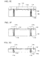
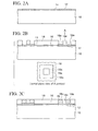
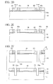
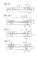
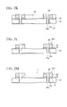
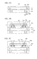
- FIG.2A to FIG.2M are sectional views showing a method of manufacturing a semiconductor device according to a first embodiment of the present invention in order of the step
- FIG.3A to FIG.3D are sectional views showing an example of a method of packaging the semiconductor device according to the first embodiment of the present invention.
- a semiconductor wafer (semiconductor substrate) 10 on which predetermined elements, multi-layered wirings (not shown), etc. are formed and which has a thickness of about 400 ⁇ m is prepared.
- Connecting pads 12 made of Al, Al alloy, Cu, or the like are formed on the element forming surface of the semiconductor wafer 10 to be exposed from the element forming surface. Portions except the connecting pads 12 are covered with a passivation film 14 made of a silicon nitride film, a polyimide resin, or the like.
- a metal film selected from a gold (Au) film, a copper (Cu) film, a nickel (Ni) film, a chromium (Cr) film, a titanium (Ti) film, a tungsten (W) film, etc. or their laminated film is used.
- the island-like patterns 18x of the dry-film resist film 18 correspond to portions in which through holes passing through the connecting pads 12, etc. are formed later, such areas are not particularly restricted as far as such areas are located within areas corresponding to the connecting pads 12.
- the island-like patterns 18x may be formed at positions which are deviated toward the peripheral side of the connecting pads 12.
- a bump metal film 20 of about 10 to 200 ⁇ m thickness is formed in the opening portions 18a in the dry-film resist film 18 by the electroplating utilizing the seed metal film 16 as a plating power-supply layer.
- the bump metal film 20 is formed like a ring in the opening portions 18a of the dry-film resist film 18 except the island-like patterns 18x over the connecting pads 12.
- the bump metal film 20 for example, an Au film, a Cu film, a Ni film/Au film laminated sequentially from the bottom, a solder film such as tin (Sn)-lead (Pb) series, etc., a Pb-free solder film such as tin (Sn)-silver (Ag) series, etc. may be employed.
- the bump metal film 20 formed in the opening portions 18a of the dry-film resist film 18 acts later as the bumps of the semiconductor chip.
- the bump metal film 20 such as an Au film, a Cu film, or the like may be formed by the electroless plating.
- the island-like patterns 18x of the dry-film resist film 18 are etched selectively by the laser while using the bump metal films 20 as a mask.
- opening portions 20a of the bump metal films 20 are exposed, and thus portions in which through holes are formed are defined in the semiconductor wafer 10.
- the seed metal film 16 exposed from the opening portions 20a of the bump metal films 20 is etched by RIE (Reactive Ion Etching), and then the underlying connecting pads 12 are etched.
- RIE reactive Ion Etching
- the RIE using a fluorine-based gas (CF 4 , etc.) is employed when the Au film is used as the seed metal film 16
- the RIE using a chlorine-based gas (Cl 2 , etc.) is employed when the Al film is used as the connecting pads 12.
- the bump metal films 20 serving as a mask and the to-be-etched seed metal film 16 it is preferable that a combination of materials having a high selective etching ratio in the RIE should be employed as the bump metal films 20 serving as a mask and the to-be-etched seed metal film 16.
- a film thickness of the bump metal films 20 is considerably larger than that of the seed metal film 16, no trouble occurs even if both films are made of the same material such as the Au film, or the like.
- the semiconductor wafer (silicon wafer) 10 is etched by the RIE using the fluorine-based gas (CF 4 , etc.) while using the bump metal films 20 and the dry-film resist film 18 as a mask.
- through holes 10a each having a depth that reaches the back surface are formed.
- the through holes 10a may be formed by the etching using the laser instead of the RIE.
- the through holes 10a each passing from an upper surface of the seed metal film 16 to the back surface of the semiconductor wafer 10 and connected to the opening portion 20a of the bump metal film 20 are formed.
- the through holes 10a containing the opening portions 20a of the bump metal films 20 are called the through holes 10a.
- the dry-film resist film 18 having the ring-like opening portions 18a in the areas that correspond to the connecting pads 12 is formed in alignment with the connecting pads 12, portions on which the bump metal film 20 is formed and portions in which the through hole 10a is formed are defined at the same time on the connecting pads 12 respectively. Then, the seed metal films 16, the connecting pads 12, and the semiconductor wafer 10 located under the island-like patterns 18x of the dry-film resist film 18 (corresponding to the opening portions 20a of the bump metal films 20) are etched, so that the through holes 10a are formed.
- the portions on which the bump metal film 20 is formed and the portions in which the through hole 10a being communicated with the opening portion 20a is formed can be defined simultaneously over the connecting pads 12 by executing one masking step. Therefore, since the number of masking steps can be reduced compared to previously-proposed methods and also only the displacement between the connecting pads 12 and the bump metal films 20 should be taken into consideration, an alignment precision between the bump metal films 20 and the through holes 10a can be improved. As a result, the bumps and the through holes that can respond to the connecting pads 12 as finer patterns can be formed easily.
- a thickness is reduced to about 150 ⁇ m or less (preferably, about 50 ⁇ m or less) by grinding the back surface of the semiconductor wafer 10 by means of the grinder.
- ground portions of the semiconductor wafer 10 are made of silicon, for example, and the material such as the Cu film that is different from the semiconductor wafer 10 is not present, such ground portions can be ground by a normal grinder without generating trouble. Therefore, unlike previously-proposed methods, there is no need to introduce a special grinder, and therefore an increase in a production cost is not brought about.
- the through holes 10a similar to those in FIG.2G may be formed by forming holes 10x each having a depth of about 150 ⁇ m or less, which does not pass through the semiconductor wafer 10, and then grinding the back surface of the semiconductor wafer 10 to expose the holes 10x.
- the holes 10x each having a depth that corresponds to a finally derived thickness of the thinned semiconductor wafer 10 may be formed, a throughput of the step of etching the semiconductor wafer 10 can be improved.
- a protection film 22 made of resin, or the like is pasted onto the bump metal films 20 and the dry-film resist film 18 over the thinned semiconductor wafer 10. At this time, the protection film 22 should be buried up to lower portions of the opening portions 20a of the bump metal films 20 or upper portions of the connecting pads 12 in the through holes 10a.
- an insulating film 24 made of a silicon oxide film, or the like is formed on inner surfaces of the through holes 10a and the back surface of the semiconductor wafer 10 by the CVD, or the like.
- the protection film 22 is released from the bump metal films 20 and the dry-film resist film 18.
- the insulating film 24 which is formed on a portion of the protection film 22 buried in the opening portions 20a of the bump metal films 20 is lifted off.
- the insulating film 24 is left selectively on side surfaces of the through holes 10a.
- This insulating film 24 is provided to isolate electrically the through wirings formed in the through holes 10a from the semiconductor wafer 10.
- the masking step is not used, and therefore the process can be simplified and a production cost can be reduced.
- the step of forming the insulating film 24 on the side surfaces of the through holes 10a may be executed before the back surface of the semiconductor wafer 10 is ground.
- through wirings 26 are formed on inner surfaces of the opening portions 20a of the bump metal films 20 and the inner surfaces of the through holes 10a by the electroplating utilizing the seed metal film 16 and the bump metal films 20 connected thereto as a plating power-supply layer.
- a metal film made of an Au film, a Cu film, or the like is used as the through wirings 26.
- the film formation is started from upper surfaces of the seed metal film 16 and the bump metal films 20 exposed from the side surfaces of the through holes 10a and side surfaces of the opening portions 20a, and then the film formation is extended toward lower sides of the through holes 10a. It is preferable that, since the plating is also applied to the upper surfaces of the bump metal films 20, the same material as that of the bump metal films 20 should be used as the material of the through wirings 26.
- a diameter of the through hole 10a is set to almost 20 to 30 ⁇ m
- a thickness of the semiconductor wafer 10 is set to almost 10 ⁇ m
- the through hole 10a is not perfectly buried by the through wiring 26 to form a cavity in its center portion.
- portions of the through wirings 26 exposed from inner peripheral portions of the through holes 10a on the back surface side of the semiconductor wafer 10 serve as connection terminals 26a on the back surface side.
- the through wiring 26 may be perfectly buried in the through holes 10a by applying the plating continuously.
- top end surfaces of the through wirings 26 exposed from bottom portions of the through holes 10a on the back surface side of the semiconductor wafer 10 serve as the connection terminals 26a on the back surface side.
- a mode (FIG.2J) in which the cavity may be formed in its center portion over the entire through hole 10a may be employed, or a mode (FIG.2K) in which the through hole 10a is buried perfectly by the through wiring 26 may be employed.
- a mode in which the opening portion 20a of the bump metal films 20 is buried by the through wiring 26 but the cavity is formed in its center portion of the through hole 10a may be employed.
- a diameter of the through hole 10a should be set smaller than a thickness of the semiconductor wafer 10.
- the diameter of the through hole 10a should be set larger than the thickness of the semiconductor wafer 10. In this manner, the diameter of the through hole 10a and the thickness of the semiconductor wafer 10 can be adjusted appropriately so as to fit in with the final shape of the through wiring 26.
- the dry-film resist film 18 is removed and then the seed metal film 16 is etched by using the bump metal films 20 as a mask.
- metal bumps 20x each consisting of the bump metal film 20 and an upper portion of the through wiring 26 are obtained.
- the metal bumps 20x on the element forming surface side of the semiconductor wafer 10 are connected electrically to the connection terminals 26a on the back surface side via the through holes 10a.
- the portions on which the metal bumps 20x are formed and the portions in which the through holes 10a are formed are defined at the same time on the connecting pads 12 respectively by applying one time the masking step onto the connecting pads 12 of the semiconductor wafer 10. Therefore, the number of masking steps can be reduced in contrast to previously-proposed methods and also the alignment precision can be improved.
- the semiconductor wafer 10 since only the semiconductor wafer 10 is ground upon grinding the back surface of the semiconductor wafer 10, the semiconductor wafer 10 can be thinned to a predetermined thickness by the normal grinding equipment without generation of any trouble.
- the chip in which the through wiring 26 is buried completely in the through holes 10a respectively is used as the semiconductor chip 1.
- a wiring substrate 40 on which the semiconductor chip 1 is mounted is prepared.
- through holes 30a are provided in a base substrate 30 made of resin, or the like.
- a through-hole plating layer 30b connected to a first wiring pattern 32 on the base substrate 30 is formed on inner surfaces of the through holes 30a respectively.
- the through holes are buried by a resin body 30c respectively.
- a first interlayer insulating film 34 made of resin such as polyimide, epoxy, or the like and having via holes 34x therein is formed on the first wiring patterns 32.
- second wiring patterns 32a connected to the first wiring patterns 32 via the via holes 34x are formed on the first interlayer insulating film 34.
- the above metal bumps 20x of the semiconductor chip 1 are flip-chip bonded to the second wiring patterns 32a of the wiring substrate 40.
- an underfill resin 17 is filled into clearances between the semiconductor chip 1 and, the second wiring patterns 32a and the first interlayer insulating film 34.
- a second interlayer insulating film 34a made of resin to cover the semiconductor chip 1 is formed.
- via holes 34y each reaching an upper surface of the connection terminal 26a of the through wiring 26 are formed by etching predetermined portions of the second interlayer insulating film 34a on the connection terminals 26a of the through wirings 26 by means of the laser, or the like.
- third wiring patterns 32b connected to the connection terminal 26a of the through wiring 26 via the via holes 34y are formed by the ordinary wiring forming method such as the semi-additive process, or the like.
- respective steps from the step of flip-chip bonding the above metal bumps 20x of the semiconductor chip 1 to the second wiring patterns 32a to the step of forming the third wiring patterns 32b may be repeated predetermined times subsequently.
- a plurality of semiconductor chips 1 are buried in the interlayer insulating film respectively and packaged three-dimensionally, and also a plurality of semiconductor chips 1 are connected mutually via the through holes 10a in the semiconductor chip 1 and the via holes formed in the interlayer insulating film.
- a solder resist film 36 having opening portions on the connection portions of the third wiring patterns 32b is formed, and then an Ni/Au film 38 is formed on the connection portions of the third wiring patterns 32b by the electroless plating.
- various packaging structures such as a structure in which the semiconductor chip 1 is not buried in the interlayer insulating film and metal bumps of another semiconductor chip are bonded directly to the connection terminals 26a on the back surface of the semiconductor chip 1, etc. may be employed.
- any of various shapes described above may be employed as the shape of the metal bumps 20x of the semiconductor chip 1.
- the metal bumps 20x of the semiconductor chip 1 are made of the Au film and the metal bumps have the cavity in their center portion (the shape in FIG.2J)
- the metal bumps 20x of the semiconductor chip 1 are bonded to Au electrodes of a wiring substrate etc. by Au-Au bonding with the ultrasonic wave
- the metal bumps 20x can be bonded simultaneously at their outer peripheries and their inner peripheries. Therefore, the mode has an advantage that the metal bumps 20x are easily bonded.
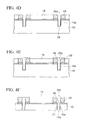
- FIG.4A to FIG.4F are sectional views showing a method of manufacturing a semiconductor device according to a second embodiment of the present invention.
- a difference of the second embodiment from the first embodiment resides in that holes not passing through the semiconductor wafer 10 are formed in advance upon forming the through holes 10a in the semiconductor wafer 10, then the through wiring is buried in the holes respectively, and then the connection terminals of the through wirings are exposed by grinding the back surface of the semiconductor wafer 10.
- the semiconductor wafer having the same structure as shown in FIG.2E is prepared by the similar method to the first embodiment.
- the semiconductor wafer 10 is etched in the middle of its thickness by using the bump metal films 20 and the dry-film resist film 18 as a mask.
- the holes 10x having a depth of about 150 ⁇ m or less are formed.
- the insulating film 24 for covering the opening portions 20a of the bump metal films 20 and the holes 10x and made of the silicon oxide film, etc. is formed on the resultant structure in FIG.4B by the CVD, or the like.
- a resist coating film 23x is formed to fill the opening portions 20a of the bump metal films 20 and the holes 10x by coating a positive resist coating liquid on the insulating film 24.
- the insulating film 24 is etched by the isotropic dry etching or the wet etching while using the resist films 23 as a mask, and then the resist film 23 is removed.
- the insulating film 24 is left selectively in the holes 10x of the semiconductor wafer 10. Like the first embodiment, this insulating film 24 is provided to isolate electrically the through wirings formed in the holes 10x from the semiconductor wafer 10.
- the through wiring 26 is formed in the opening portions 20a of the bump metal films 20 and the holes 10x by the electroplating in the similar way to the first embodiment.
- the through wiring 26 may be formed into various shapes explained in the first embodiment.
- the holes 10x formed in the semiconductor wafer 10 act as the through holes 10a that connect the element forming surface side and the back surface side of the semiconductor wafer 10.
- the dry-film resist film 18 is removed, and then the metal bumps 20x are obtained by etching the seed metal film 16 while using the bump metal films 20 as a mask.
- the metal bumps 20x connected to the connecting pads 12 are connected electrically to the connection terminals 26a on the back surface side via the through holes 10a.
- the removal of the dry-film resist film 18 and the etching of the seed metal film 16 may be carried out before the back surface of the semiconductor wafer 10 is ground.
- individual semiconductor chips 1a semiconductor devices that are divided into individual pieces are obtained by dicing the semiconductor wafer 10.
Landscapes
- Internal Circuitry In Semiconductor Integrated Circuit Devices (AREA)
Applications Claiming Priority (2)
| Application Number | Priority Date | Filing Date | Title |
|---|---|---|---|
| JP2003007461 | 2003-01-15 | ||
| JP2003007461A JP4322508B2 (ja) | 2003-01-15 | 2003-01-15 | 半導体装置の製造方法 |
Publications (3)
| Publication Number | Publication Date |
|---|---|
| EP1439576A2 true EP1439576A2 (de) | 2004-07-21 |
| EP1439576A3 EP1439576A3 (de) | 2007-04-25 |
| EP1439576B1 EP1439576B1 (de) | 2012-02-22 |
Family
ID=32588516
Family Applications (1)
| Application Number | Title | Priority Date | Filing Date |
|---|---|---|---|
| EP04250045A Expired - Lifetime EP1439576B1 (de) | 2003-01-15 | 2004-01-07 | Verfahren zur Herstellung eines Durchgangsloches |
Country Status (3)
| Country | Link |
|---|---|
| US (1) | US6831000B2 (de) |
| EP (1) | EP1439576B1 (de) |
| JP (1) | JP4322508B2 (de) |
Cited By (9)
| Publication number | Priority date | Publication date | Assignee | Title |
|---|---|---|---|---|
| EP1760775A1 (de) * | 2005-08-29 | 2007-03-07 | Shinko Electric Industries Co., Ltd. | Halbleiterbauelement mit Durchgangselektrode und dessen Herstellung |
| EP1653508A3 (de) * | 2004-10-26 | 2009-08-12 | Sanyo Electric Co., Ltd. | Halbleitervorrichtung und Verfahren zu Ihrer Herstellung |
| US7646100B2 (en) | 2004-10-28 | 2010-01-12 | Sanyo Electric Co., Ltd. | Semiconductor device with penetrating electrode |
| US7670955B2 (en) | 2004-10-26 | 2010-03-02 | Sanyo Electric Co., Ltd. | Semiconductor device and manufacturing method of the same |
| US7732925B2 (en) | 2004-02-17 | 2010-06-08 | Sanyo Electric Co., Ltd. | Semiconductor device and manufacturing method thereof |
| EP1768177A3 (de) * | 2005-09-21 | 2011-06-22 | Shinko Electric Industries Co., Ltd. | Verfahren zur Herstellung eines Halbleiterchips |
| EP2267895B1 (de) * | 2004-09-13 | 2012-11-14 | Seiko Epson Corporation | Elektronisches Bauelement, Leiterplatte, elektronisches Gerät und Herstellungsverfahren des elektronischen Bauelements |
| WO2013106796A1 (en) * | 2012-01-13 | 2013-07-18 | Qualcomm Incorporated | Integrating through substrate vias into middle-of-line layers of integrated circuits |
| US9165898B2 (en) | 2005-03-10 | 2015-10-20 | Semiconductor Components Industries, Llc | Method of manufacturing semiconductor device with through hole |
Families Citing this family (44)
| Publication number | Priority date | Publication date | Assignee | Title |
|---|---|---|---|---|
| US8084866B2 (en) | 2003-12-10 | 2011-12-27 | Micron Technology, Inc. | Microelectronic devices and methods for filling vias in microelectronic devices |
| US7091124B2 (en) | 2003-11-13 | 2006-08-15 | Micron Technology, Inc. | Methods for forming vias in microelectronic devices, and methods for packaging microelectronic devices |
| TWI303491B (en) * | 2004-02-20 | 2008-11-21 | Toshiba Kk | Semiconductor relay apparatus and wiring board fabrication method |
| JP4556454B2 (ja) * | 2004-03-15 | 2010-10-06 | パナソニック電工株式会社 | 半導体装置の製造方法 |
| US20050247894A1 (en) | 2004-05-05 | 2005-11-10 | Watkins Charles M | Systems and methods for forming apertures in microfeature workpieces |
| US7232754B2 (en) * | 2004-06-29 | 2007-06-19 | Micron Technology, Inc. | Microelectronic devices and methods for forming interconnects in microelectronic devices |
| US7425499B2 (en) | 2004-08-24 | 2008-09-16 | Micron Technology, Inc. | Methods for forming interconnects in vias and microelectronic workpieces including such interconnects |
| SG120200A1 (en) | 2004-08-27 | 2006-03-28 | Micron Technology Inc | Slanted vias for electrical circuits on circuit boards and other substrates |
| US7300857B2 (en) * | 2004-09-02 | 2007-11-27 | Micron Technology, Inc. | Through-wafer interconnects for photoimager and memory wafers |
| CN100525097C (zh) * | 2004-09-13 | 2009-08-05 | 精工爱普生株式会社 | 电子零件和电子零件的制造方法 |
| US7271482B2 (en) | 2004-12-30 | 2007-09-18 | Micron Technology, Inc. | Methods for forming interconnects in microelectronic workpieces and microelectronic workpieces formed using such methods |
| JP4434965B2 (ja) * | 2005-01-11 | 2010-03-17 | 株式会社東芝 | 半導体装置 |
| US20060160346A1 (en) * | 2005-01-19 | 2006-07-20 | Intel Corporation | Substrate bump formation |
| US20060177999A1 (en) * | 2005-02-10 | 2006-08-10 | Micron Technology, Inc. | Microelectronic workpieces and methods for forming interconnects in microelectronic workpieces |
| TW200644261A (en) * | 2005-06-06 | 2006-12-16 | Megica Corp | Chip-package structure and manufacturing process thereof |
| US7946331B2 (en) | 2005-06-14 | 2011-05-24 | Cufer Asset Ltd. L.L.C. | Pin-type chip tooling |
| US8456015B2 (en) | 2005-06-14 | 2013-06-04 | Cufer Asset Ltd. L.L.C. | Triaxial through-chip connection |
| US7795134B2 (en) | 2005-06-28 | 2010-09-14 | Micron Technology, Inc. | Conductive interconnect structures and formation methods using supercritical fluids |
| JP4533283B2 (ja) * | 2005-08-29 | 2010-09-01 | 新光電気工業株式会社 | 半導体装置の製造方法 |
| JP4828182B2 (ja) * | 2005-08-31 | 2011-11-30 | 新光電気工業株式会社 | 半導体装置の製造方法 |
| US7622377B2 (en) | 2005-09-01 | 2009-11-24 | Micron Technology, Inc. | Microfeature workpiece substrates having through-substrate vias, and associated methods of formation |
| US7262134B2 (en) | 2005-09-01 | 2007-08-28 | Micron Technology, Inc. | Microfeature workpieces and methods for forming interconnects in microfeature workpieces |
| US7863187B2 (en) | 2005-09-01 | 2011-01-04 | Micron Technology, Inc. | Microfeature workpieces and methods for forming interconnects in microfeature workpieces |
| US7772115B2 (en) * | 2005-09-01 | 2010-08-10 | Micron Technology, Inc. | Methods for forming through-wafer interconnects, intermediate structures so formed, and devices and systems having at least one solder dam structure |
| US8154105B2 (en) * | 2005-09-22 | 2012-04-10 | International Rectifier Corporation | Flip chip semiconductor device and process of its manufacture |
| CN101375146B (zh) * | 2006-01-19 | 2010-08-11 | 株式会社藤仓 | 压力传感器封装体和电子器件 |
| US7892972B2 (en) * | 2006-02-03 | 2011-02-22 | Micron Technology, Inc. | Methods for fabricating and filling conductive vias and conductive vias so formed |
| US7749899B2 (en) | 2006-06-01 | 2010-07-06 | Micron Technology, Inc. | Microelectronic workpieces and methods and systems for forming interconnects in microelectronic workpieces |
| US7629249B2 (en) | 2006-08-28 | 2009-12-08 | Micron Technology, Inc. | Microfeature workpieces having conductive interconnect structures formed by chemically reactive processes, and associated systems and methods |
| US7902643B2 (en) | 2006-08-31 | 2011-03-08 | Micron Technology, Inc. | Microfeature workpieces having interconnects and conductive backplanes, and associated systems and methods |
| WO2008083284A2 (en) * | 2006-12-29 | 2008-07-10 | Cufer Asset Ltd. L.L.C. | Front-end processed wafer having through-chip connections |
| JP4353263B2 (ja) * | 2007-03-16 | 2009-10-28 | セイコーエプソン株式会社 | 半導体装置の製造方法及び半導体装置 |
| KR100897761B1 (ko) | 2007-05-21 | 2009-05-15 | 박태석 | 관통 비아홀 공정을 이용한 실리콘 이미지 센서의 웨이퍼레벨 패키지 및 그 제조방법 |
| SG150410A1 (en) | 2007-08-31 | 2009-03-30 | Micron Technology Inc | Partitioned through-layer via and associated systems and methods |
| KR100886720B1 (ko) * | 2007-10-30 | 2009-03-04 | 주식회사 하이닉스반도체 | 적층 반도체 패키지 및 이의 제조 방법 |
| US7884015B2 (en) | 2007-12-06 | 2011-02-08 | Micron Technology, Inc. | Methods for forming interconnects in microelectronic workpieces and microelectronic workpieces formed using such methods |
| JP4781440B2 (ja) * | 2009-02-05 | 2011-09-28 | ソニー エリクソン モバイル コミュニケーションズ, エービー | 画像撮影装置、画像撮影装置の制御方法及び制御プログラム |
| US8415805B2 (en) * | 2010-12-17 | 2013-04-09 | Skyworks Solutions, Inc. | Etched wafers and methods of forming the same |
| JP5313294B2 (ja) * | 2011-05-16 | 2013-10-09 | 新光電気工業株式会社 | 半導体装置 |
| JP5521130B1 (ja) * | 2012-08-30 | 2014-06-11 | パナソニック株式会社 | 電子部品パッケージおよびその製造方法 |
| US9449937B2 (en) | 2012-09-05 | 2016-09-20 | Panasonic Intellectual Property Management Co., Ltd. | Semiconductor device and method for manufacturing the same |
| JP7070848B2 (ja) * | 2018-07-26 | 2022-05-18 | 住友電工デバイス・イノベーション株式会社 | 半導体装置の製造方法 |
| JP7176169B2 (ja) * | 2019-02-28 | 2022-11-22 | 住友電工デバイス・イノベーション株式会社 | 半導体装置の製造方法及び半導体装置 |
| WO2022137347A1 (ja) * | 2020-12-22 | 2022-06-30 | 三菱電機株式会社 | 半導体装置及びその製造方法 |
Citations (6)
| Publication number | Priority date | Publication date | Assignee | Title |
|---|---|---|---|---|
| JPS59222954A (ja) | 1983-06-01 | 1984-12-14 | Hitachi Ltd | 積層半導体集積回路およびその製法 |
| JPS6188546A (ja) | 1984-10-05 | 1986-05-06 | Fujitsu Ltd | 半導体装置 |
| JPS63156348A (ja) | 1986-12-19 | 1988-06-29 | Fujitsu Ltd | 半導体装置 |
| US4978639A (en) | 1989-01-10 | 1990-12-18 | Avantek, Inc. | Method for the simultaneous formation of via-holes and wraparound plating on semiconductor chips |
| JP2000286304A (ja) | 1999-03-31 | 2000-10-13 | Seiko Epson Corp | 半導体素子の製造方法、および半導体素子、および半導体装置の製造方法、および半導体装置、ならびに実装モジュール |
| EP1267402A2 (de) | 2001-06-14 | 2002-12-18 | Shinko Electric Industries Co. Ltd. | Halbleiter und seine Herstellung |
Family Cites Families (3)
| Publication number | Priority date | Publication date | Assignee | Title |
|---|---|---|---|---|
| US5686067A (en) * | 1995-01-05 | 1997-11-11 | Isp Investments Inc. | Low voc hair spray compositions |
| US6620731B1 (en) * | 1997-12-18 | 2003-09-16 | Micron Technology, Inc. | Method for fabricating semiconductor components and interconnects with contacts on opposing sides |
| US6693358B2 (en) * | 2000-10-23 | 2004-02-17 | Matsushita Electric Industrial Co., Ltd. | Semiconductor chip, wiring board and manufacturing process thereof as well as semiconductor device |
-
2003
- 2003-01-15 JP JP2003007461A patent/JP4322508B2/ja not_active Expired - Fee Related
-
2004
- 2004-01-05 US US10/750,905 patent/US6831000B2/en not_active Expired - Lifetime
- 2004-01-07 EP EP04250045A patent/EP1439576B1/de not_active Expired - Lifetime
Patent Citations (6)
| Publication number | Priority date | Publication date | Assignee | Title |
|---|---|---|---|---|
| JPS59222954A (ja) | 1983-06-01 | 1984-12-14 | Hitachi Ltd | 積層半導体集積回路およびその製法 |
| JPS6188546A (ja) | 1984-10-05 | 1986-05-06 | Fujitsu Ltd | 半導体装置 |
| JPS63156348A (ja) | 1986-12-19 | 1988-06-29 | Fujitsu Ltd | 半導体装置 |
| US4978639A (en) | 1989-01-10 | 1990-12-18 | Avantek, Inc. | Method for the simultaneous formation of via-holes and wraparound plating on semiconductor chips |
| JP2000286304A (ja) | 1999-03-31 | 2000-10-13 | Seiko Epson Corp | 半導体素子の製造方法、および半導体素子、および半導体装置の製造方法、および半導体装置、ならびに実装モジュール |
| EP1267402A2 (de) | 2001-06-14 | 2002-12-18 | Shinko Electric Industries Co. Ltd. | Halbleiter und seine Herstellung |
Cited By (14)
| Publication number | Priority date | Publication date | Assignee | Title |
|---|---|---|---|---|
| US7732925B2 (en) | 2004-02-17 | 2010-06-08 | Sanyo Electric Co., Ltd. | Semiconductor device and manufacturing method thereof |
| US7750478B2 (en) | 2004-02-17 | 2010-07-06 | Sanyo Electric Co., Ltd. | Semiconductor device with via hole of uneven width |
| EP2267895B1 (de) * | 2004-09-13 | 2012-11-14 | Seiko Epson Corporation | Elektronisches Bauelement, Leiterplatte, elektronisches Gerät und Herstellungsverfahren des elektronischen Bauelements |
| US7670955B2 (en) | 2004-10-26 | 2010-03-02 | Sanyo Electric Co., Ltd. | Semiconductor device and manufacturing method of the same |
| US7582971B2 (en) | 2004-10-26 | 2009-09-01 | Sanyo Electric Co., Ltd. | Semiconductor device and manufacturing method of the same |
| EP1653508A3 (de) * | 2004-10-26 | 2009-08-12 | Sanyo Electric Co., Ltd. | Halbleitervorrichtung und Verfahren zu Ihrer Herstellung |
| US7646100B2 (en) | 2004-10-28 | 2010-01-12 | Sanyo Electric Co., Ltd. | Semiconductor device with penetrating electrode |
| US9165898B2 (en) | 2005-03-10 | 2015-10-20 | Semiconductor Components Industries, Llc | Method of manufacturing semiconductor device with through hole |
| US7605080B2 (en) | 2005-08-29 | 2009-10-20 | Shinko Electric Industries Co., Ltd. | Semiconductor device and method of manufacturing the same |
| EP1760775A1 (de) * | 2005-08-29 | 2007-03-07 | Shinko Electric Industries Co., Ltd. | Halbleiterbauelement mit Durchgangselektrode und dessen Herstellung |
| EP1768177A3 (de) * | 2005-09-21 | 2011-06-22 | Shinko Electric Industries Co., Ltd. | Verfahren zur Herstellung eines Halbleiterchips |
| WO2013106796A1 (en) * | 2012-01-13 | 2013-07-18 | Qualcomm Incorporated | Integrating through substrate vias into middle-of-line layers of integrated circuits |
| US8975729B2 (en) | 2012-01-13 | 2015-03-10 | Qualcomm Incorporated | Integrating through substrate vias into middle-of-line layers of integrated circuits |
| EP3731265A1 (de) * | 2012-01-13 | 2020-10-28 | QUALCOMM Incorporated | Integration von substratdurchkontaktierungen in middle-of-line schichten von integrierten schaltkreisen |
Also Published As
| Publication number | Publication date |
|---|---|
| US20040137661A1 (en) | 2004-07-15 |
| US6831000B2 (en) | 2004-12-14 |
| EP1439576A3 (de) | 2007-04-25 |
| JP2004221357A (ja) | 2004-08-05 |
| EP1439576B1 (de) | 2012-02-22 |
| JP4322508B2 (ja) | 2009-09-02 |
Similar Documents
| Publication | Publication Date | Title |
|---|---|---|
| US6831000B2 (en) | Semiconductor device manufacturing method | |
| US12444719B2 (en) | Package and manufacturing method thereof | |
| CN109585404B (zh) | 半导体封装及其形成方法 | |
| TWI691026B (zh) | 製造半導體元件的方法 | |
| CN110970407B (zh) | 集成电路封装件和方法 | |
| TWI719730B (zh) | 積體電路封裝及其製作方法 | |
| CN109786350B (zh) | 半导体封装件和方法 | |
| KR101041011B1 (ko) | 전자 부품 실장 구조 및 그 제조 방법 | |
| TWI446491B (zh) | 半導體封裝及其製造方法 | |
| KR100621438B1 (ko) | 감광성 폴리머를 이용한 적층 칩 패키지 및 그의 제조 방법 | |
| US12362262B2 (en) | Semiconductor device including through die via | |
| EP1427006A1 (de) | Verpackungsstruktur für elektronische Bauteile und Methode zu deren Herstellung | |
| US20060019467A1 (en) | Methods of fabricating integrated circuit chips for multi-chip packaging and wafers and chips formed thereby | |
| KR102949219B1 (ko) | 반도체 디바이스 및 반도체 디바이스 제조 방법 | |
| CN117766514A (zh) | 具有边缘侧互连的半导体封装及半导体封装组合件以及其形成方法 | |
| TW202008481A (zh) | 形成半導體封裝體的方法 | |
| TW202543078A (zh) | 半導體晶粒的封裝結構及其形成方法 | |
| CN110556354B (zh) | 封装件基板及其制造方法 | |
| US20210134752A1 (en) | Semiconductor device package and method of manufacturing the same | |
| KR20190091095A (ko) | 반도체 패키지 및 이의 제조 방법 | |
| CN115513149A (zh) | 半导体封装及其形成方法 | |
| TWI871916B (zh) | 半導體封裝結構的製備方法 | |
| US20250349775A1 (en) | Microbump structure with enclosed joint window | |
| TW202520486A (zh) | 半導體封裝結構 | |
| KR20240164417A (ko) | 집적 회로 패키지 및 그 형성 방법 |
Legal Events
| Date | Code | Title | Description |
|---|---|---|---|
| PUAI | Public reference made under article 153(3) epc to a published international application that has entered the european phase |
Free format text: ORIGINAL CODE: 0009012 |
|
| AK | Designated contracting states |
Kind code of ref document: A2 Designated state(s): AT BE BG CH CY CZ DE DK EE ES FI FR GB GR HU IE IT LI LU MC NL PT RO SE SI SK TR |
|
| AX | Request for extension of the european patent |
Extension state: AL LT LV MK |
|
| PUAL | Search report despatched |
Free format text: ORIGINAL CODE: 0009013 |
|
| AK | Designated contracting states |
Kind code of ref document: A3 Designated state(s): AT BE BG CH CY CZ DE DK EE ES FI FR GB GR HU IE IT LI LU MC NL PT RO SE SI SK TR |
|
| AX | Request for extension of the european patent |
Extension state: AL LT LV MK |
|
| 17P | Request for examination filed |
Effective date: 20071017 |
|
| AKX | Designation fees paid |
Designated state(s): DE |
|
| 17Q | First examination report despatched |
Effective date: 20100201 |
|
| GRAP | Despatch of communication of intention to grant a patent |
Free format text: ORIGINAL CODE: EPIDOSNIGR1 |
|
| GRAS | Grant fee paid |
Free format text: ORIGINAL CODE: EPIDOSNIGR3 |
|
| GRAA | (expected) grant |
Free format text: ORIGINAL CODE: 0009210 |
|
| AK | Designated contracting states |
Kind code of ref document: B1 Designated state(s): DE |
|
| REG | Reference to a national code |
Ref country code: DE Ref legal event code: R096 Ref document number: 602004036568 Country of ref document: DE Effective date: 20120419 |
|
| PLBE | No opposition filed within time limit |
Free format text: ORIGINAL CODE: 0009261 |
|
| STAA | Information on the status of an ep patent application or granted ep patent |
Free format text: STATUS: NO OPPOSITION FILED WITHIN TIME LIMIT |
|
| 26N | No opposition filed |
Effective date: 20121123 |
|
| REG | Reference to a national code |
Ref country code: DE Ref legal event code: R097 Ref document number: 602004036568 Country of ref document: DE Effective date: 20121123 |
|
| REG | Reference to a national code |
Ref country code: DE Ref legal event code: R082 Ref document number: 602004036568 Country of ref document: DE Representative=s name: HL KEMPNER PATENTANWALT, RECHTSANWALT, SOLICIT, DE |
|
| PGFP | Annual fee paid to national office [announced via postgrant information from national office to epo] |
Ref country code: DE Payment date: 20211130 Year of fee payment: 19 |
|
| REG | Reference to a national code |
Ref country code: DE Ref legal event code: R119 Ref document number: 602004036568 Country of ref document: DE |
|
| PG25 | Lapsed in a contracting state [announced via postgrant information from national office to epo] |
Ref country code: DE Free format text: LAPSE BECAUSE OF NON-PAYMENT OF DUE FEES Effective date: 20230801 |