EP2461352A1 - Verfahren zur Herstellung von Kontakten mit geringem Widerstand auf n-Germanium - Google Patents
Verfahren zur Herstellung von Kontakten mit geringem Widerstand auf n-Germanium Download PDFInfo
- Publication number
- EP2461352A1 EP2461352A1 EP11191678A EP11191678A EP2461352A1 EP 2461352 A1 EP2461352 A1 EP 2461352A1 EP 11191678 A EP11191678 A EP 11191678A EP 11191678 A EP11191678 A EP 11191678A EP 2461352 A1 EP2461352 A1 EP 2461352A1
- Authority
- EP
- European Patent Office
- Prior art keywords
- layer
- silicon layer
- interfacial
- doped
- ωcm
- Prior art date
- Legal status (The legal status is an assumption and is not a legal conclusion. Google has not performed a legal analysis and makes no representation as to the accuracy of the status listed.)
- Granted
Links
Images

Classifications
-
- H—ELECTRICITY
- H10—SEMICONDUCTOR DEVICES; ELECTRIC SOLID-STATE DEVICES NOT OTHERWISE PROVIDED FOR
- H10D—INORGANIC ELECTRIC SEMICONDUCTOR DEVICES
- H10D64/00—Electrodes of devices having potential barriers
- H10D64/01—Manufacture or treatment
- H10D64/011—Manufacture or treatment of electrodes ohmically coupled to a semiconductor
- H10D64/0111—Manufacture or treatment of electrodes ohmically coupled to a semiconductor to Group IV semiconductors
- H10D64/0113—Manufacture or treatment of electrodes ohmically coupled to a semiconductor to Group IV semiconductors the conductive layers comprising highly doped semiconductor materials, e.g. polysilicon layers or amorphous silicon layers
Definitions
- the present invention relates to electrical contacting of n-type germanium with a conductive material with electrical resistivity smaller than 1x10 -2 ⁇ cm, such as for example a metal or a metal silicide.
- the present invention relates to a method for manufacturing contacts on n-type germanium, having a contact resistivity below 10 -4 ⁇ cm 2 , for example below 10 -5 ⁇ cm 2 .
- the present invention relates to devices thus obtained.
- Non-ohmic or high resistivity contacts having a contact resistivity higher than 10 -4 ⁇ cm 2 are a roadblock to applications of germanium (Ge) despite its high potential for e.g. Complementary Metal Oxide Semiconductor (CMOS) transistors or memory elements. Both CMOS applications on Ge and Ge selector diodes for memory elements need low contact resistivity.
- germanium Ge
- CMOS Complementary Metal Oxide Semiconductor
- Ge shows a depinning factor of about 0.05 and a charge neutrality level of 0.09 eV, which means Fermi level pinning close to the top of the valence band.
- n-Ge contacts are difficult to form because of low activation limits and concentration enhanced diffusion of n-type dopants in Ge. Barrier height lowering by means of thin oxides/nitrides was reported, but the contact resistivity obtained was about 1 ⁇ 10 -2 ⁇ cm 2 .
- the present invention provides a method for manufacturing an electrical contact between n-type germanium and a layer of material with electrical resistivity smaller than 1x10 -2 ⁇ cm, such as for example a metal layer or a metal silicide layer.
- the method comprises obtaining a semiconductor substrate having atop a germanium region doped with n-type dopants at a first doping level; forming an interfacial silicon layer overlying the n-type doped germanium region, the interfacial silicon layer being doped with n-type dopants at a second doping level and having a thickness higher than the critical thickness of silicon on germanium, such that the interfacial layer is at least partially relaxed; and forming a layer of material with electrical resistivity smaller than 1x10 -2 ⁇ cm overlying the interfacial silicon layer.
- the interfacial Si layer will be also referred as Si-passivation layer.
- the interfacial Si layer may be completely covering the n-type doped Ge.
- the interfacial Si layer can be formed by any deposition technique for example selected from Chemical Vapour Deposition (CVD), Low Pressure Chemical Vapour Deposition CVD (LPCVD), Physical Vapour Deposition (PVD), Molecular Beam Epitaxy (MBE) or any other deposition/growth technique suitable to form a polycrystalline or a monocrystalline silicon layer.
- CVD Chemical Vapour Deposition
- LPCVD Low Pressure Chemical Vapour Deposition CVD
- PVD Physical Vapour Deposition
- MBE Molecular Beam Epitaxy
- forming an interfacial silicon layer may comprise forming a silicon layer with a thickness between a few monolayers, such as for example five or ten monolayers, and 50 nm.
- the interfacial silicon layer has a thickness lower than 50nm, for example lower than 30nm, such as for example lower than 20nm.
- the interfacial Si layer has a thickness higher than the critical thickness of silicon on germanium.
- the critical thickness depends on the lattice-mismatch between the material to be grown/deposited and the material of the substrate (underlying the material to be grown).
- layers with a thickness smaller than the critical thickness are strained, since a certain amount of elastic strain can be accommodated by any material without generating dislocations or defects.
- the interfacial Si layer is not fully strained, but at least partially relaxed due to the defects present in the layer.
- the at least partial relaxation is related to a lower electron barrier at the interface between n-type doped Ge and the Si interfacial layer.
- the interfacial Si layer is doped with a n-type dopant such as for example P, As or Sb or any combination thereof.
- the doping level of the interfacial Si layer may be higher than the doping level of the underlying n-type doped Ge.
- the second doping level of the interfacial silicon layer may be at least 1x10 19 cm -3 .
- forming the interfacial silicon layer doped with n-type dopants at the second doping level may comprises introducing n-type dopants into the interfacial silicon layer during formation thereof, e.g. during growth or deposition thereof, by an in-situ doping technique with suitable precursors.
- forming an interfacial silicon layer may comprise forming a monocrystalline silicon layer.
- forming an interfacial silicon layer may comprise forming a polycrystalline silicon layer.
- a monocrystalline silicon layer may be preferred over a polycrystalline silicon layer, as the latter has some roughness and needs to be thicker to form a closed layer.
- polycrystalline silicon might be deposited in a non-epi tool, which might have some manufacturing advantages.
- the layer is at least partially relaxed comprising defects which have a beneficial effect for the method of the present invention.
- the n-doped underlying germanium layer/region may either be monocrystalline or polycrystalline and can be formed on a semiconductor substrate such as a silicon wafer. In different embodiments of the present invention the n-type doped germanium layer/region is part of a device.
- the growth of the n-doped germanium region can be either selective or non-selective.
- the interfacial Si layer is formed by selective epitaxial growth only on the n-doped germanium region to be contacted.
- n-type germanium is doped with n-type species such as phosphorous, arsenic or antimony or any combinations thereof.
- the layer overlying the silicon interfacial layer is made of a highly conductive material (i.e. a material with electrical resistivity smaller than 1x10 -2 ⁇ cm) such as a metal, a metal silicide.
- the layer of material with electrical resistivity smaller than 1x10 -2 ⁇ cm can comprise a plurality of layers of made of such a highly conductive material.
- the layer of material with electrical resistivity smaller than 1x10 -2 ⁇ cm is a stack of Ti/TiN.
- the interfacial Si layer can be partly consumed to form a silicide as contact metal.
- the present invention provides a semiconductor device comprising a germanium region doped with n-type dopants at a first doping level; on the germanium region, an interfacial silicon layer doped with n-type dopants at a second doping level, and having a thickness higher than the critical thickness, such that the interfacial layer is at least partially relaxed; and a layer of material with electrical resistivity smaller than 1x10 -2 ⁇ cm overlying the interfacial silicon layer.
- the interfacial silicon layer may have a thickness between a few monolayers, e.g. five or ten monolayers, and 50 nm.
- the interfacial silicon layer may have a second doping level higher than the first doping level of the germanium region.
- the second doping level of the interfacial silicon layer may be at least 1x10 19 cm -3 .
- the interfacial silicon layer may be a monocrystalline layer or a polycrystalline layer.
- the n-doped underlying germanium region may either be monocrystalline or polycrystalline.
- the germanium region may be (part of) a germanium substrate, or it and can be formed on a semiconductor substrate such as a silicon wafer.
- the n-type doped germanium region is part of a semiconductor device.
- contact resistivity refers to the contribution to the total resistance of a material which emanates from contacting two different types of materials, in particular n-type Germanium and a material with electrical resistivity smaller than 1x10 -2 ⁇ cm, such as e.g. a metal or a metal silicide, as opposed to the intrinsic resistivity which is an inherent property of each of the materials.
- the contact resistivity is the resistivity at the level of the conductive material-semiconductor interface.
- critical thickness of a semiconductor layer is the thickness below which no dislocation occurs if this layer is provided on a lattice-mismatched layer, and above which dislocations do occur.
- a certain amount of elastic strain can be accommodated by any material without generating dislocations or defects, if its thickness is below the critical thickness. It takes energy to accommodate a layer of lattice-mismatched material. The energy depends on the thickness and the size of the lattice mismatch. It also requires energy to create a dislocation that will relieve the lattice mismatch strain. If the thickness of the semiconductor layer is kept small enough to maintain the elastic strain energy below the energy of dislocation formation (smaller than the critical thickness), a strained-layer structure is formed. If the thickness of the semiconductor layer is larger than the critical thickness, this layer will at least partly relax.
- Different embodiments of the present invention describe a method for manufacturing electrical contacts between n-type germanium and a layer of material with electrical resistivity smaller than 1x10 -2 ⁇ cm, the electrical contacts having a low specific contact resistivity, e.g. a specific contact resistivity below 10 -4 ⁇ cm 2 , such as for example below 10 -5 ⁇ cm 2 .
- the electrical contacts having a low specific contact resistivity are ohmic contacts having a specific contact resistivity ⁇ c lower than 2 ⁇ 10 -6 ⁇ cm 2 .
- an ohmic contact is a region on a semiconductor device that has been prepared so that the current-voltage (I-V) curve of the device is linear and symmetric. If the I-V characteristic is non-linear and asymmetric, the contact is not ohmic, but is a Schottky contact. Low-resistance, stable contacts are critical for the performance and reliability of integrated circuits and their preparation and characterization are major efforts in circuit fabrication.
- n-type germanium crystalline or poly-crystalline
- a material with electrical resistivity smaller than 1x10 -2 ⁇ cm have typically a high contact resistivity (higher than 10 -4 ⁇ cm 2 ) which is due to Fermi-level pinning and to a low activation of donors in germanium.
- a known method to lower the high contact resistivity between n-type germanium and metal is by increasing the activated doping density in germanium by using e.g. laser annealing.
- the laser annealing typically requires high temperatures (above 700°C) which are incompatible with low temperature processing of advanced devices.
- the present invention describes a method for manufacturing electrical contacts between n-type germanium and a highly conductive material with electrical resistivity smaller than 1x10 -2 ⁇ cm, the electrical contacts having a specific contact resistivity below 10 -4 ⁇ cm 2 , the method comprising:
- the germanium region may be a germanium substrate; in this case "a semiconductor substrate having atop a n-type doped germanium region" may in its entirety be a germanium substrate.
- the germanium region may be a germanium layer, patterned or unpatterned, provided on top of another suitable substrate, for example a semiconductor substrate, such as for example a silicon or a silicon germanium substrate.
- a semiconductor substrate such as for example a silicon or a silicon germanium substrate.
- the present invention is, however, not limited to these types of substrates, and the substrate can be made of any suitable material or combination of (layers of) material onto which a germanium region can be provided.
- a thin in-situ doped epitaxial Si-passivation layer is grown selectively on n-type doped Ge substrate.
- the dopants of the Si layer are n-type dopants, such as e.g. phosphorus, and, in the embodiment described, are provided at a dopant level of 1 ⁇ 10 20 cm -3 .
- the selective growing of Si on the n-type doped Ge substrate in the example described is followed by a Ti/TiN metal stack deposition.
- the insertion of the thin Si-passivation layer reduces the pinning and activation limitation, achieving contact resistivity values of about 1 ⁇ 10 -6 ⁇ cm 2 .
- sample fabrication was started by growing 1 ⁇ m of in-situ n-type (P) doped Ge 10 with a doping level of 1 ⁇ 10 19 cm -3 on a 3x10 14 cm -3 p-Si substrate (not illustrated in FIG. 1 ) at 450°C.
- P in-situ n-type
- a post epitaxial anneal was performed after n-type Ge growth to reduce defects.
- Reference samples were prepared according to known methods, e.g. an As implant (5 ⁇ 10 15 cm -2 , 9 keV) followed by a thermal treatment (anneal) at 600 °C for about 5 minutes. This "soak" anneal results in activation levels lower than 1 ⁇ 10 19 cm -3 .
- a Si interfacial layer 11 was grown selectively only on the n-type doped germanium 10 of the contact areas.
- a cleaning step in the example illustrated a HF-based cleaning step, was performed on the Ge substrate.
- a thermal treatment (bake) was performed at 650 °C in the presence of H 2 .
- the Si interfacial layer 11 was epitaxially grown at 550 °C for 12 min and, respectively, 15 min using dichlorosilane as precursor.
- the layer 11 was in-situ doped with PH 3 to a doping density of about 1x10 20 cm -3 . Resulting thicknesses were about 10 nm and, respectively, 16 nm, as determined by Transmission Electron Microscopy (TEM).
- TEM Transmission Electron Microscopy
- FIG. 1 (bottom) represents a cross-section TEM picture and shows the integrity of the sample with a 10 nm doped epitaxial crystalline Si interfacial layer 11.
- the dark area near the interface between the Si layer 11 and the Ge layer 10, and the uneven contrast in the Si layer 11 are due to strain and defects.
- the HAADF-STEM (High Angle Annular Dark Field - Scanning Transmission Electron Microscopy) image at the top right of FIG. 1 shows the smoothness of the Si/Ge interface and the rough nature of the Si/Ti interface. No interlayers of an unexpected phase (such as oxides or silicides) are observed with STEM, Energy Dispersive Spectrometry (EDS) and Electron Energy Loss Spectroscopy (EELS, not shown).
- EDS Energy Dispersive Spectrometry
- EELS Electron Energy Loss Spectroscopy
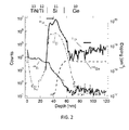
- FIG. 2 a Secondary Ion Mass Spectroscopy (SIMS) depth profile is shown of the n-type doped Ge 10/n-type doped Si 11/ Ti 12 sample.
- Phosphorous (P) concentration is about 1x10 20 cm -3 in the grown Si 11 and about 1x10 19 cm -3 in the bulk Ge 10.
- the results in Figure 2 shows that P remains confined in the Si-layer 11 and reaches about 3x10 18 cm -3 at the Si/Ge interface with little intermixing into the underlying Ge 10.
- the decreased concentration of P near the Ge/Si interface is due to outdiffusion during the post-annealing step after Ge-epitaxial growth of the Ge substrate.
- Physical characterization techniques show the integrity of the contact stack and no unexpected phases.
- CTLM contact resistance circular transmission line method measurements
- the resistance of the structures depends on radius (r 1 ) and slit width (r 2 - r 1 ).
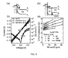
- the CTLM resistance model suitable for a wide range of specific contact resistivities ⁇ c consists of the contact resistances R c1 (eq. 1) of the inner contact (see circuit schematic in FIG. 3 ), R c2 (eq. 2) of the outer contact, the structure sheet resistance of the Ge (R ss ) (eq. 3) and a constant parasitic resistance R para due to cabling, probe contacts etc. (not shown in FIG. 3 ).
- R c ⁇ 1 ⁇ c 2 ⁇ ⁇ ⁇ r 1 ⁇ L T ⁇ I 0 r 1 L T / I 1 r 1 L T
- R c ⁇ 2 ⁇ c 2 ⁇ ⁇ ⁇ r 2 ⁇ L T ⁇ K 0 r 2 L T / K 1 r 2 L T
- LT (eq. 4) is the transfer length and I 0 , I 1 , K 0 , K 1 are Bessel functions. This model is fitted to the resistance of measured structures of different geometries to determine the specific contact resistivity ⁇ c and the Ge sheet resistivity (R s ).
- FIG.4 shows the band diagrams for: (a) prior art n-type Ge/Ti contacts; and (b) n-type Ge/n-type epi-Si layer/ Ti contacts in accordance with embodiments of the present invention.
- CTLM resistance model fit to the data of the Si passivated sample in accordance with embodiments of the present invention is shown in FIG. 4(d) .
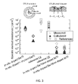
- the specific contact resistivities are shown in FIG.3 .
- a physical model of the contact resistivity ⁇ c was developed.
- the physical model for n-type Ge contact resistivity ⁇ c takes into account field emission and thermionic field emission including the effect of image-force barrier lowering.
- FIG. 3 Also some reference values from literature have been added to FIG. 3 .
- an insulator inserted between the doped germanium and the electrode material with electrical resistivity smaller than 1x10 -2 ⁇ cm was used.
- the doping density (1 ⁇ 10 19 cm -3 ) is of a similar order as the Ge doping density of embodiments of the present invention.
- FIG. 3 shows the extracted specific contact resistivities for in-situ doped Ge/Ti/TiN, in-situ doped Ge followed by As implant and 5 min anneal/Ti/TiN and in-situ doped Ge/Al, samples from Ref. [3] ( Lee et al., Applied Physics Letters 96, 052514 (2010 )) and Ref. [2] (Kobayashi et al., Proceedings of the Symposium on VLSI Tech (2008)) and Si-passivated samples according to embodiments of the present invention. Values measured (open diamonds) are in good agreement with values calculated using a physical model of ⁇ c (full triangles).
- FIG. 3 the extracted specific contact resistivities are shown for the samples with doped Si passivation layer in accordance with embodiments of the present invention.
- ⁇ c 1.4 ⁇ 10 -6 ⁇ cm 2 for the 10 nm Si sample and 1.7 ⁇ 10 -6 ⁇ cm 2 for the 16 nm sample.
- the specific contact resistivity ⁇ c is 1 to 2 ⁇ 10 -7 ⁇ cm 2 which is comparable but still somewhat lower than the observed value for Si-passivated germanium in accordance with embodiments of the present invention.
- n-Ge contacts In n-Ge contacts thermionic emission dominates conduction due to the high Schottky barrier height and limited activated doping level ( FIG. 4(a) ). n-Ge contacts without the interfacial Si layer typically show Schottky diode I-V characteristics.
- FIG. 4(b) The expected nature of an n-Ge contact with an inserted interfacial Si layer in accordance with embodiments of the present invention is illustrated in FIG. 4(b) .
- the barrier height for bulk Si/Ti is 0.5 eV -0.6 eV, which is lower than or similar compared to 0.57 eV for Ge/Ti. The difference is not large even though Si shows a depinning factor of about 0.27.
- the activated doping is higher compared to any of the n-Ge samples, causing tunneling to dominate and material-with-electrical-resistivity-smaller-than-1x10 -2 - ⁇ cm'---to-Si contacts to be ohmic and low resistive.
- the electron barrier at the Si-Ge interface is about 0.55eV.
- the Si is expected to be (partially) relaxed.
- relaxed Si on Ge shows a small difference (50meV) in electron affinity and hence a small electron barrier.
- the low values of the specific contact resistivity ⁇ c obtained with the method of embodiments of the present invention correlate with the fact that the interface corresponds to the (partially) relaxed case.
- the modelling shows that given a Ge doping level of 3 ⁇ 10 18 cm -3 the Si-Ge barrier has to be lower than 0.23 eV to obtain ⁇ c lower than 1 ⁇ 10 -6 ⁇ cm 2 .
- the slightly higher specific contact resistivity ⁇ c obtained with the method of embodiments of the present invention when compared to calculated values for Ti/bulk Si contacts shown in FIG. 3 might be due to defects and/or slight band misalignments due to strain built up by lattice mismatch at or near the Ge/Si interface.
- the low specific contact resistivity ⁇ c to n-doped Ge ( ⁇ c ⁇ 2 ⁇ 10 -6 ⁇ cm 2 ) obtained with the method of embodiments of the present invention demonstrates the possibility of eliminating Fermi level pinning and dopant activation limits in n-Ge contacts. This is a significant improvement compared to typical best values of about 10 -4 ⁇ cm 2 achieved by previously reported techniques, opening the opportunity to implement Ge in advanced CMOS and memory applications.
Landscapes
- Electrodes Of Semiconductors (AREA)
Applications Claiming Priority (1)
| Application Number | Priority Date | Filing Date | Title |
|---|---|---|---|
| US42008110P | 2010-12-06 | 2010-12-06 |
Publications (2)
| Publication Number | Publication Date |
|---|---|
| EP2461352A1 true EP2461352A1 (de) | 2012-06-06 |
| EP2461352B1 EP2461352B1 (de) | 2013-07-10 |
Family
ID=45418365
Family Applications (1)
| Application Number | Title | Priority Date | Filing Date |
|---|---|---|---|
| EP11191678.9A Active EP2461352B1 (de) | 2010-12-06 | 2011-12-02 | Verfahren zur Herstellung von Kontakten mit geringem Widerstand auf n-Germanium |
Country Status (3)
| Country | Link |
|---|---|
| US (1) | US9177812B2 (de) |
| EP (1) | EP2461352B1 (de) |
| JP (1) | JP5926045B2 (de) |
Families Citing this family (8)
| Publication number | Priority date | Publication date | Assignee | Title |
|---|---|---|---|---|
| US9692209B2 (en) * | 2011-06-10 | 2017-06-27 | Massachusetts Institute Of Technology | High-concentration active doping in semiconductors and semiconductor devices produced by such doping |
| JP2014041987A (ja) * | 2012-08-24 | 2014-03-06 | Shimane Univ | n+型Ge半導体層形成方法およびオーミック接触構造 |
| US9449885B1 (en) | 2015-06-19 | 2016-09-20 | International Business Machines Corporation | High germanium content FinFET devices having the same contact material for nFET and pFET devices |
| US10748776B2 (en) | 2016-09-01 | 2020-08-18 | Japan Science And Technology Agency | Semiconductor device including contact structure |
| JP2018082036A (ja) | 2016-11-16 | 2018-05-24 | ルネサスエレクトロニクス株式会社 | 半導体装置 |
| US10797137B2 (en) | 2017-06-30 | 2020-10-06 | Taiwan Semiconductor Manufacturing Co., Ltd. | Method for reducing Schottky barrier height and semiconductor device with reduced Schottky barrier height |
| CN109473468A (zh) * | 2018-10-26 | 2019-03-15 | 中国科学院微电子研究所 | 半导体器件与其制作方法 |
| US10937654B2 (en) | 2019-01-24 | 2021-03-02 | Micron Technology, Inc. | Methods of doping a silicon-containing material and methods of forming a semiconductor device |
Citations (3)
| Publication number | Priority date | Publication date | Assignee | Title |
|---|---|---|---|---|
| US5563448A (en) * | 1993-03-02 | 1996-10-08 | Samsung Electronics Co., Ltd. | Ohmic contact structure of a highly integrated semiconductor device having two resistance control layers formed between a metal electrode and the substrate |
| EP1447839A1 (de) * | 2001-08-06 | 2004-08-18 | Sumitomo Mitsubishi Silicon Corporation | Halbleitersubstrat, feldeffekttransistor und verfahren zu ihrer herstellung |
| US20060073664A1 (en) * | 2004-10-05 | 2006-04-06 | Masao Kondo | Semiconductor device and manufacturing method of the same |
Family Cites Families (15)
| Publication number | Priority date | Publication date | Assignee | Title |
|---|---|---|---|---|
| JPS618916A (ja) * | 1984-06-21 | 1986-01-16 | インタ−ナシヨナル・ビジネス・マシ−ンズ・コ−ポレ−シヨン | ド−プ領域の形成方法 |
| US4999685A (en) | 1989-05-16 | 1991-03-12 | United States Of America As Represented By The Secretary Of The Air Force | Schotiky barrier height for metal contacts to III-V semiconductor compounds |
| JPH03110837A (ja) * | 1989-09-26 | 1991-05-10 | Seiko Instr Inc | 半導体装置の製造方法 |
| US5801444A (en) * | 1989-09-29 | 1998-09-01 | International Business Machines Corporation | Multilevel electronic structures containing copper layer and copper-semiconductor layers |
| US5063174A (en) | 1990-09-18 | 1991-11-05 | Polaroid Corporation | Si/Au/Ni alloyed ohmic contact to n-GaAs and fabricating process therefor |
| US5168330A (en) | 1990-12-03 | 1992-12-01 | Research Triangle Institute | Semiconductor device having a semiconductor substrate interfaced to a dissimilar material by means of a single crystal pseudomorphic interlayer |
| JP2877108B2 (ja) * | 1996-12-04 | 1999-03-31 | 日本電気株式会社 | 半導体装置およびその製造方法 |
| ATE346410T1 (de) * | 2000-08-04 | 2006-12-15 | Amberwave Systems Corp | Siliziumwafer mit monolithischen optoelektronischen komponenten |
| US6511905B1 (en) * | 2002-01-04 | 2003-01-28 | Promos Technologies Inc. | Semiconductor device with Si-Ge layer-containing low resistance, tunable contact |
| US7964789B2 (en) | 2003-05-07 | 2011-06-21 | Imec | Germanium solar cell and method for the production thereof |
| US7132338B2 (en) * | 2003-10-10 | 2006-11-07 | Applied Materials, Inc. | Methods to fabricate MOSFET devices using selective deposition process |
| JP4636227B2 (ja) * | 2004-01-19 | 2011-02-23 | セイコーエプソン株式会社 | 半導体装置の製造方法 |
| JP5047486B2 (ja) | 2004-10-13 | 2012-10-10 | アイメック | 半導体デバイスの製造方法 |
| US20070262296A1 (en) * | 2006-05-11 | 2007-11-15 | Matthias Bauer | Photodetectors employing germanium layers |
| EP1883103A3 (de) * | 2006-07-27 | 2008-03-05 | Interuniversitair Microelektronica Centrum | Abscheidung von III-Nitriden auf Ge |
-
2011
- 2011-12-02 EP EP11191678.9A patent/EP2461352B1/de active Active
- 2011-12-05 US US13/310,945 patent/US9177812B2/en active Active
- 2011-12-05 JP JP2011265947A patent/JP5926045B2/ja active Active
Patent Citations (3)
| Publication number | Priority date | Publication date | Assignee | Title |
|---|---|---|---|---|
| US5563448A (en) * | 1993-03-02 | 1996-10-08 | Samsung Electronics Co., Ltd. | Ohmic contact structure of a highly integrated semiconductor device having two resistance control layers formed between a metal electrode and the substrate |
| EP1447839A1 (de) * | 2001-08-06 | 2004-08-18 | Sumitomo Mitsubishi Silicon Corporation | Halbleitersubstrat, feldeffekttransistor und verfahren zu ihrer herstellung |
| US20060073664A1 (en) * | 2004-10-05 | 2006-04-06 | Masao Kondo | Semiconductor device and manufacturing method of the same |
Non-Patent Citations (2)
| Title |
|---|
| KOBAYASHI ET AL., PROCEEDINGS OF THE SYMPOSIUM ON VLSI TECH, 2008 |
| LEE ET AL., APPLIED PHYSICS LETTERS, vol. 96, 2010, pages 052514 |
Also Published As
| Publication number | Publication date |
|---|---|
| EP2461352B1 (de) | 2013-07-10 |
| US20120138928A1 (en) | 2012-06-07 |
| US9177812B2 (en) | 2015-11-03 |
| JP2012124483A (ja) | 2012-06-28 |
| JP5926045B2 (ja) | 2016-05-25 |
Similar Documents
| Publication | Publication Date | Title |
|---|---|---|
| EP2461352B1 (de) | Verfahren zur Herstellung von Kontakten mit geringem Widerstand auf n-Germanium | |
| US6534871B2 (en) | Device including an epitaxial nickel silicide on (100) Si or stable nickel silicide on amorphous Si and a method of fabricating the same | |
| TWI665717B (zh) | 半導體元件及其製造方法 | |
| US10680081B2 (en) | Vertical transistors with improved top source/drain junctions | |
| EP2162921B1 (de) | Sperrschichtdiode mit verringertem sperrstrom | |
| JP2001024194A (ja) | 半導体装置の製造方法及び半導体装置 | |
| Salm et al. | Diffusion and Electrical Properties of Boron and Arsenic Doped Poly‐Si and Poly‐Ge x Si1− x (x∼ 0.3) as Gate Material for Sub‐0.25 μm Complementary Metal Oxide Semiconductor Applications | |
| Ye et al. | High tensile strained in-situ phosphorus doped silicon epitaxial film for nMOS applications | |
| US9105571B2 (en) | Interface engineering to optimize metal-III-V contacts | |
| KR100942965B1 (ko) | 스트레인드채널을 갖는 반도체소자 및 그 제조 방법 | |
| Onga et al. | Characterization of polycrystalline silicon MOS transistors and its film properties. I | |
| US9911873B2 (en) | Hydrogenation of passivated contacts | |
| Porret et al. | Very low temperature epitaxy of group-IV semiconductors for use in FinFET, stacked nanowires and monolithic 3D integration | |
| US20160300925A1 (en) | Low resistance contact for semiconductor devices | |
| Ye et al. | Activation and deactivation in ultra-highly doped n-type epitaxy for NMOS applications | |
| EP0779652A2 (de) | Verfahren zur Herstellung eines Heteroübergang-Bipolartransistors | |
| US9985159B2 (en) | Passivated contact formation using ion implantation | |
| CN114050115A (zh) | 缺陷检测方法、存储器及其制作方法 | |
| CN101217157A (zh) | 包含多晶硅的半导体器件及其制造方法 | |
| CN116830280A (zh) | 具有优化的金属触点的锗光电二极管 | |
| Yu et al. | High performance n-MOSFETs with novel source/drain on selectively grown Ge on Si for monolithic integration | |
| Loubet et al. | Optimization of SiC: P Raised Source Drain Epitaxy for Planar 20nm Fully Depleted SOI MOSFET Structures | |
| Deprat et al. | Investigation of Arsenic Transient Enhanced Diffusion From Emitter Process at 550° C Si: As RP-CVD Epitaxy Using Disilane Precursor | |
| Zaima et al. | challenges and developments in Gesn process technology for Si nanoelectronics | |
| Cabaret et al. | Impact of Rapid Thermal Annealing on Tensily-Strained Phosphorous-Doped Si for Advanced FD-SOI Nodes |
Legal Events
| Date | Code | Title | Description |
|---|---|---|---|
| PUAI | Public reference made under article 153(3) epc to a published international application that has entered the european phase |
Free format text: ORIGINAL CODE: 0009012 |
|
| AK | Designated contracting states |
Kind code of ref document: A1 Designated state(s): AL AT BE BG CH CY CZ DE DK EE ES FI FR GB GR HR HU IE IS IT LI LT LU LV MC MK MT NL NO PL PT RO RS SE SI SK SM TR |
|
| AX | Request for extension of the european patent |
Extension state: BA ME |
|
| 17P | Request for examination filed |
Effective date: 20121203 |
|
| GRAP | Despatch of communication of intention to grant a patent |
Free format text: ORIGINAL CODE: EPIDOSNIGR1 |
|
| GRAS | Grant fee paid |
Free format text: ORIGINAL CODE: EPIDOSNIGR3 |
|
| GRAA | (expected) grant |
Free format text: ORIGINAL CODE: 0009210 |
|
| AK | Designated contracting states |
Kind code of ref document: B1 Designated state(s): AL AT BE BG CH CY CZ DE DK EE ES FI FR GB GR HR HU IE IS IT LI LT LU LV MC MK MT NL NO PL PT RO RS SE SI SK SM TR |
|
| REG | Reference to a national code |
Ref country code: GB Ref legal event code: FG4D |
|
| REG | Reference to a national code |
Ref country code: CH Ref legal event code: EP Ref country code: AT Ref legal event code: REF Ref document number: 621383 Country of ref document: AT Kind code of ref document: T Effective date: 20130715 |
|
| REG | Reference to a national code |
Ref country code: IE Ref legal event code: FG4D |
|
| REG | Reference to a national code |
Ref country code: DE Ref legal event code: R096 Ref document number: 602011002288 Country of ref document: DE Effective date: 20130905 |
|
| PG25 | Lapsed in a contracting state [announced via postgrant information from national office to epo] |
Ref country code: SI Free format text: LAPSE BECAUSE OF FAILURE TO SUBMIT A TRANSLATION OF THE DESCRIPTION OR TO PAY THE FEE WITHIN THE PRESCRIBED TIME-LIMIT Effective date: 20130710 |
|
| REG | Reference to a national code |
Ref country code: AT Ref legal event code: MK05 Ref document number: 621383 Country of ref document: AT Kind code of ref document: T Effective date: 20130710 |
|
| REG | Reference to a national code |
Ref country code: NL Ref legal event code: VDEP Effective date: 20130710 |
|
| REG | Reference to a national code |
Ref country code: LT Ref legal event code: MG4D |
|
| PG25 | Lapsed in a contracting state [announced via postgrant information from national office to epo] |
Ref country code: NO Free format text: LAPSE BECAUSE OF FAILURE TO SUBMIT A TRANSLATION OF THE DESCRIPTION OR TO PAY THE FEE WITHIN THE PRESCRIBED TIME-LIMIT Effective date: 20131010 Ref country code: AT Free format text: LAPSE BECAUSE OF FAILURE TO SUBMIT A TRANSLATION OF THE DESCRIPTION OR TO PAY THE FEE WITHIN THE PRESCRIBED TIME-LIMIT Effective date: 20130710 Ref country code: LT Free format text: LAPSE BECAUSE OF FAILURE TO SUBMIT A TRANSLATION OF THE DESCRIPTION OR TO PAY THE FEE WITHIN THE PRESCRIBED TIME-LIMIT Effective date: 20130710 Ref country code: SE Free format text: LAPSE BECAUSE OF FAILURE TO SUBMIT A TRANSLATION OF THE DESCRIPTION OR TO PAY THE FEE WITHIN THE PRESCRIBED TIME-LIMIT Effective date: 20130710 Ref country code: PT Free format text: LAPSE BECAUSE OF FAILURE TO SUBMIT A TRANSLATION OF THE DESCRIPTION OR TO PAY THE FEE WITHIN THE PRESCRIBED TIME-LIMIT Effective date: 20131111 Ref country code: IS Free format text: LAPSE BECAUSE OF FAILURE TO SUBMIT A TRANSLATION OF THE DESCRIPTION OR TO PAY THE FEE WITHIN THE PRESCRIBED TIME-LIMIT Effective date: 20131110 Ref country code: CY Free format text: LAPSE BECAUSE OF FAILURE TO SUBMIT A TRANSLATION OF THE DESCRIPTION OR TO PAY THE FEE WITHIN THE PRESCRIBED TIME-LIMIT Effective date: 20130828 Ref country code: BE Free format text: LAPSE BECAUSE OF FAILURE TO SUBMIT A TRANSLATION OF THE DESCRIPTION OR TO PAY THE FEE WITHIN THE PRESCRIBED TIME-LIMIT Effective date: 20130710 Ref country code: HR Free format text: LAPSE BECAUSE OF FAILURE TO SUBMIT A TRANSLATION OF THE DESCRIPTION OR TO PAY THE FEE WITHIN THE PRESCRIBED TIME-LIMIT Effective date: 20130710 |
|
| PG25 | Lapsed in a contracting state [announced via postgrant information from national office to epo] |
Ref country code: ES Free format text: LAPSE BECAUSE OF FAILURE TO SUBMIT A TRANSLATION OF THE DESCRIPTION OR TO PAY THE FEE WITHIN THE PRESCRIBED TIME-LIMIT Effective date: 20131021 Ref country code: LV Free format text: LAPSE BECAUSE OF FAILURE TO SUBMIT A TRANSLATION OF THE DESCRIPTION OR TO PAY THE FEE WITHIN THE PRESCRIBED TIME-LIMIT Effective date: 20130710 Ref country code: PL Free format text: LAPSE BECAUSE OF FAILURE TO SUBMIT A TRANSLATION OF THE DESCRIPTION OR TO PAY THE FEE WITHIN THE PRESCRIBED TIME-LIMIT Effective date: 20130710 Ref country code: FI Free format text: LAPSE BECAUSE OF FAILURE TO SUBMIT A TRANSLATION OF THE DESCRIPTION OR TO PAY THE FEE WITHIN THE PRESCRIBED TIME-LIMIT Effective date: 20130710 Ref country code: NL Free format text: LAPSE BECAUSE OF FAILURE TO SUBMIT A TRANSLATION OF THE DESCRIPTION OR TO PAY THE FEE WITHIN THE PRESCRIBED TIME-LIMIT Effective date: 20130710 Ref country code: GR Free format text: LAPSE BECAUSE OF FAILURE TO SUBMIT A TRANSLATION OF THE DESCRIPTION OR TO PAY THE FEE WITHIN THE PRESCRIBED TIME-LIMIT Effective date: 20131011 |
|
| PG25 | Lapsed in a contracting state [announced via postgrant information from national office to epo] |
Ref country code: CY Free format text: LAPSE BECAUSE OF FAILURE TO SUBMIT A TRANSLATION OF THE DESCRIPTION OR TO PAY THE FEE WITHIN THE PRESCRIBED TIME-LIMIT Effective date: 20130710 |
|
| PG25 | Lapsed in a contracting state [announced via postgrant information from national office to epo] |
Ref country code: CZ Free format text: LAPSE BECAUSE OF FAILURE TO SUBMIT A TRANSLATION OF THE DESCRIPTION OR TO PAY THE FEE WITHIN THE PRESCRIBED TIME-LIMIT Effective date: 20130710 Ref country code: SK Free format text: LAPSE BECAUSE OF FAILURE TO SUBMIT A TRANSLATION OF THE DESCRIPTION OR TO PAY THE FEE WITHIN THE PRESCRIBED TIME-LIMIT Effective date: 20130710 Ref country code: RO Free format text: LAPSE BECAUSE OF FAILURE TO SUBMIT A TRANSLATION OF THE DESCRIPTION OR TO PAY THE FEE WITHIN THE PRESCRIBED TIME-LIMIT Effective date: 20130710 Ref country code: DK Free format text: LAPSE BECAUSE OF FAILURE TO SUBMIT A TRANSLATION OF THE DESCRIPTION OR TO PAY THE FEE WITHIN THE PRESCRIBED TIME-LIMIT Effective date: 20130710 Ref country code: EE Free format text: LAPSE BECAUSE OF FAILURE TO SUBMIT A TRANSLATION OF THE DESCRIPTION OR TO PAY THE FEE WITHIN THE PRESCRIBED TIME-LIMIT Effective date: 20130710 |
|
| PLBE | No opposition filed within time limit |
Free format text: ORIGINAL CODE: 0009261 |
|
| STAA | Information on the status of an ep patent application or granted ep patent |
Free format text: STATUS: NO OPPOSITION FILED WITHIN TIME LIMIT |
|
| PG25 | Lapsed in a contracting state [announced via postgrant information from national office to epo] |
Ref country code: IT Free format text: LAPSE BECAUSE OF FAILURE TO SUBMIT A TRANSLATION OF THE DESCRIPTION OR TO PAY THE FEE WITHIN THE PRESCRIBED TIME-LIMIT Effective date: 20130710 |
|
| 26N | No opposition filed |
Effective date: 20140411 |
|
| REG | Reference to a national code |
Ref country code: DE Ref legal event code: R097 Ref document number: 602011002288 Country of ref document: DE Effective date: 20140411 |
|
| PG25 | Lapsed in a contracting state [announced via postgrant information from national office to epo] |
Ref country code: LU Free format text: LAPSE BECAUSE OF FAILURE TO SUBMIT A TRANSLATION OF THE DESCRIPTION OR TO PAY THE FEE WITHIN THE PRESCRIBED TIME-LIMIT Effective date: 20131202 |
|
| REG | Reference to a national code |
Ref country code: IE Ref legal event code: MM4A |
|
| PG25 | Lapsed in a contracting state [announced via postgrant information from national office to epo] |
Ref country code: IE Free format text: LAPSE BECAUSE OF NON-PAYMENT OF DUE FEES Effective date: 20131202 |
|
| PG25 | Lapsed in a contracting state [announced via postgrant information from national office to epo] |
Ref country code: MC Free format text: LAPSE BECAUSE OF FAILURE TO SUBMIT A TRANSLATION OF THE DESCRIPTION OR TO PAY THE FEE WITHIN THE PRESCRIBED TIME-LIMIT Effective date: 20130710 |
|
| PG25 | Lapsed in a contracting state [announced via postgrant information from national office to epo] |
Ref country code: SM Free format text: LAPSE BECAUSE OF FAILURE TO SUBMIT A TRANSLATION OF THE DESCRIPTION OR TO PAY THE FEE WITHIN THE PRESCRIBED TIME-LIMIT Effective date: 20130710 |
|
| PG25 | Lapsed in a contracting state [announced via postgrant information from national office to epo] |
Ref country code: TR Free format text: LAPSE BECAUSE OF FAILURE TO SUBMIT A TRANSLATION OF THE DESCRIPTION OR TO PAY THE FEE WITHIN THE PRESCRIBED TIME-LIMIT Effective date: 20130710 |
|
| PG25 | Lapsed in a contracting state [announced via postgrant information from national office to epo] |
Ref country code: BG Free format text: LAPSE BECAUSE OF FAILURE TO SUBMIT A TRANSLATION OF THE DESCRIPTION OR TO PAY THE FEE WITHIN THE PRESCRIBED TIME-LIMIT Effective date: 20130710 Ref country code: RS Free format text: LAPSE BECAUSE OF FAILURE TO SUBMIT A TRANSLATION OF THE DESCRIPTION OR TO PAY THE FEE WITHIN THE PRESCRIBED TIME-LIMIT Effective date: 20131010 Ref country code: MK Free format text: LAPSE BECAUSE OF FAILURE TO SUBMIT A TRANSLATION OF THE DESCRIPTION OR TO PAY THE FEE WITHIN THE PRESCRIBED TIME-LIMIT Effective date: 20130710 Ref country code: HU Free format text: LAPSE BECAUSE OF FAILURE TO SUBMIT A TRANSLATION OF THE DESCRIPTION OR TO PAY THE FEE WITHIN THE PRESCRIBED TIME-LIMIT; INVALID AB INITIO Effective date: 20111202 |
|
| REG | Reference to a national code |
Ref country code: CH Ref legal event code: PL |
|
| PG25 | Lapsed in a contracting state [announced via postgrant information from national office to epo] |
Ref country code: MT Free format text: LAPSE BECAUSE OF FAILURE TO SUBMIT A TRANSLATION OF THE DESCRIPTION OR TO PAY THE FEE WITHIN THE PRESCRIBED TIME-LIMIT Effective date: 20130710 |
|
| PG25 | Lapsed in a contracting state [announced via postgrant information from national office to epo] |
Ref country code: CH Free format text: LAPSE BECAUSE OF NON-PAYMENT OF DUE FEES Effective date: 20141231 Ref country code: LI Free format text: LAPSE BECAUSE OF NON-PAYMENT OF DUE FEES Effective date: 20141231 |
|
| REG | Reference to a national code |
Ref country code: FR Ref legal event code: PLFP Year of fee payment: 5 |
|
| REG | Reference to a national code |
Ref country code: FR Ref legal event code: PLFP Year of fee payment: 6 |
|
| REG | Reference to a national code |
Ref country code: FR Ref legal event code: PLFP Year of fee payment: 7 |
|
| PG25 | Lapsed in a contracting state [announced via postgrant information from national office to epo] |
Ref country code: AL Free format text: LAPSE BECAUSE OF FAILURE TO SUBMIT A TRANSLATION OF THE DESCRIPTION OR TO PAY THE FEE WITHIN THE PRESCRIBED TIME-LIMIT Effective date: 20130710 |
|
| P01 | Opt-out of the competence of the unified patent court (upc) registered |
Effective date: 20230513 |
|
| REG | Reference to a national code |
Ref country code: DE Ref legal event code: R079 Ref document number: 602011002288 Country of ref document: DE Free format text: PREVIOUS MAIN CLASS: H01L0021285000 Ipc: H10D0064010000 |
|
| PGFP | Annual fee paid to national office [announced via postgrant information from national office to epo] |
Ref country code: DE Payment date: 20251126 Year of fee payment: 15 |
|
| PGFP | Annual fee paid to national office [announced via postgrant information from national office to epo] |
Ref country code: GB Payment date: 20251119 Year of fee payment: 15 |
|
| PGFP | Annual fee paid to national office [announced via postgrant information from national office to epo] |
Ref country code: FR Payment date: 20251120 Year of fee payment: 15 |