EP1449905A1 - Phosphore vert contenant un oxyde - Google Patents
Phosphore vert contenant un oxyde Download PDFInfo
- Publication number
- EP1449905A1 EP1449905A1 EP04002915A EP04002915A EP1449905A1 EP 1449905 A1 EP1449905 A1 EP 1449905A1 EP 04002915 A EP04002915 A EP 04002915A EP 04002915 A EP04002915 A EP 04002915A EP 1449905 A1 EP1449905 A1 EP 1449905A1
- Authority
- EP
- European Patent Office
- Prior art keywords
- phosphor
- green
- oxide phosphor
- green oxide
- pdp
- Prior art date
- Legal status (The legal status is an assumption and is not a legal conclusion. Google has not performed a legal analysis and makes no representation as to the accuracy of the status listed.)
- Granted
Links
Images



Classifications
-
- C—CHEMISTRY; METALLURGY
- C09—DYES; PAINTS; POLISHES; NATURAL RESINS; ADHESIVES; COMPOSITIONS NOT OTHERWISE PROVIDED FOR; APPLICATIONS OF MATERIALS NOT OTHERWISE PROVIDED FOR
- C09K—MATERIALS FOR MISCELLANEOUS APPLICATIONS, NOT PROVIDED FOR ELSEWHERE
- C09K11/00—Luminescent materials, e.g. electroluminescent or chemiluminescent
- C09K11/08—Luminescent materials, e.g. electroluminescent or chemiluminescent containing inorganic luminescent materials
- C09K11/77—Luminescent materials, e.g. electroluminescent or chemiluminescent containing inorganic luminescent materials containing rare earth metals
- C09K11/7728—Luminescent materials, e.g. electroluminescent or chemiluminescent containing inorganic luminescent materials containing rare earth metals containing europium
- C09K11/7734—Aluminates
-
- C—CHEMISTRY; METALLURGY
- C09—DYES; PAINTS; POLISHES; NATURAL RESINS; ADHESIVES; COMPOSITIONS NOT OTHERWISE PROVIDED FOR; APPLICATIONS OF MATERIALS NOT OTHERWISE PROVIDED FOR
- C09K—MATERIALS FOR MISCELLANEOUS APPLICATIONS, NOT PROVIDED FOR ELSEWHERE
- C09K11/00—Luminescent materials, e.g. electroluminescent or chemiluminescent
- C09K11/08—Luminescent materials, e.g. electroluminescent or chemiluminescent containing inorganic luminescent materials
- C09K11/70—Luminescent materials, e.g. electroluminescent or chemiluminescent containing inorganic luminescent materials containing phosphorus
- C09K11/71—Luminescent materials, e.g. electroluminescent or chemiluminescent containing inorganic luminescent materials containing phosphorus also containing alkaline earth metals
Definitions
- the present invention relates to a phosphor, and more particularly, to a green oxide phosphor that has improved chemical stability as well as improved luminance.
- phosphor indicates a material emitting visible ray when the phosphor excited by an electromagnetic wave such as an ultraviolet ray, an electron ray or an X-ray, transits to a ground state back.
- electromagnetic wave such as an ultraviolet ray, an electron ray or an X-ray
- Various phosphors have been developed. These phosphors have metal oxide, sulfide, acid sulfide, halide, or the like as a host lattice and emit near ultraviolet ray or visible ray due to the above-mentioned electromagnetic wave.
- the phosphors are widely used in a fluorescent lamp, a radioactive ray intensifying screen, an indoor/outdoor decoration fluorescent tile, and a display device, such as a cathode ray tube (CRT), a vacuum fluorescent display (VFD) or a plasma display panel (PDP).
- a display device such as a cathode ray tube (CRT), a vacuum fluorescent display (VFD) or a plasma display panel (PDP).
- a vacuum ultraviolet ray of 147 nm allows the phosphor to emit light so that an image is displayed.
- the vacuum ultraviolet ray is generated when inert mixed gases, such as He + Xe, Ne + Xe and He + Xe + Ne are discharged. Since the PDP can be easily made in a slim and large-sized structure, it attracts attention as a large-sized flat panel display.
- the PDP begins to be produced commercially in Korea and Japan, and extends its market share, and the image quality of the PDP continues to be improved thanks to the advancing of its technology.
- a discharge cell of a three-electrode AC surface discharge type PDP includes a pair of sustain electrodes 9 formed on an upper substrate 1 and an address electrode X formed on a lower substrate 2.
- Each of the pair of sustain electrodes 3 includes a transparent electrode 9a of Indium-Tin-Oxide (ITO) and a metal bus electrode 9b formed on an edge of the transparent electrode 9a and having a narrower width than the transparent electrode 9a.
- the metal bus electrode 9b is formed by sequentially depositing Cr/Cu/Cr and etching the deposited Cr/Cu/Cr.
- An upper dielectric layer 6 and a passivation layer 7 are deposited on the upper substrate 1 on which the pair of sustain electrodes 9 are formed, by using a screen printing process or a vacuum deposition process. Wall charges generated during plasma discharge are accumulated on the upper dielectric layer 6.
- the passivation layer 7 is formed on the upper dielectric layer 6 at a thickness of about 5000 ⁇ so as to protect the upper dielectric layer 6 and the pair of sustain electrodes 9 from damages caused by sputtering during plasma discharge and to enhance a discharge efficiency of secondary electrons.
- magnesium oxide (MgO) is used for the passivation layer 7.
- Y represents a scan sustain electrode and Z represents a common sustain electrode.
- a lower dielectric layer 4 and a barrier rib 3 are formed on a lower substrate on which an address electrode X is formed.
- a phosphor 5 is formed on the surfaces of the lower dielectric layer 4 and the barrier rib 3 by a screen printing process.
- the address electrode X is perpendicular to the sustain electrode pair 9.
- the barrier rib 3 is formed by a screen printing or a molding process to prevent ultraviolet rays and visible rays generated during discharge from leaking to an adjacent discharge cell.
- the phosphor 5 is excited by a vacuum ultraviolet ray to emit one visible ray of any one of red, green and blue. The vacuum ultraviolet ray is generated during plasma discharge of the mixed gases injected into the discharge cell.
- the PDP is time-division driven by dividing one frame into several sub-fields having different emission frequencies. Each sub-field is divided into an initialization period, an address period and an sustain period. In the initialization period, a full screen is initialized. In the address period, a scan line is selected and a cell is selected in the selected scan line. In the sustain period, the gray scale is realized according to discharge rate.
- a frame period (16.67 ms) corresponding to 1/60 second is divided into eight sub-fields SF1 to SF8 as shown in FIG. 2.
- Each of the eight sub-fields SF1 to SF8 is divided into the initialization period, the address period and the sustain period as described above.
- the phosphor 5 is excited by the vacuum ultraviolet ray to emit light, and is classified into a red phosphor, a green phosphor and a blue phosphor according to the wavelength of the emitted light.
- the red phosphor widely used in the PDP has a composition of (Ygd)BO 3 :Eu 3+
- the blue phosphor has a composition of BaMgAl 10 O 17 :Eu 2+
- the green phosphor has a composition of Zn 2 SiO 4 :Mn 2+ .
- Such phosphors are coated on the barrier rib 3 of the PDP and directly exposed to mixed gases filled in a discharge cell. If the mixed gases emit vacuum ultraviolet ray during plasma discharge, each of the phosphors emits red, green and blue lights.
- the conventional green phosphor since the green phosphor with the composition of Zn 2 SiO 4 :Mn 2+ is long in afterglow time during which green light continues to be maintained after the green light is emitted, an afterimage is left on the PDP screen. Consequently, the conventional green phosphor deteriorates the display quality of the PDP. In addition, since the dielectric characteristic and the surface characteristic of the conventional green phosphor are not excellent, the conventional green phosphor has a discharge delay problem that discharge is not generated in time. Since the conventional green phosphor has a high threshold voltage to emit the light, that is, a high discharge voltage, its power consumption is increased. Hence, it is an urgent subject to develop the phosphor with a short afterglow time, excellent dielectric characteristic and excellent surface characteristic so as to improve the display quality of the PDP and to reduce the consumption power.
- the present invention is directed to a green oxide phosphor that substantially obviates one or more problems due to limitations and disadvantages of the related art.
- a green oxide phosphor for emitting a visible ray has a general composition formula of Mg 1-(x+y) Al 2 O 4 :Eux 2+ , M y 2+ .
- Eu +2 is doped into a crystal of Mg 1-(x+y) Al 2 O 4 as an activator; and Mn +2 is added as a co-dopant.
- M is at least one selected from the group consisting of alkaline earth metals and transition metals such as Ca, Ba, Sr, Cu and Zn having a valence of +2.
- X and Y are numbers ranged from 0 to 0.9999 respectively.
- the sum of X and Y is in the range from 0 to 0.9999.
- FIG. 1 is a perspective view of a structure of a discharge cell of the conventional three-electrode AC surface discharge type plasma display panel
- FIG. 2 illustrates a frame for representing 256 gray scales of a general plasma display panel
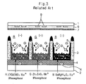
- FIG. 3 is a cross-sectional view of a phosphor coated on a discharge cell of the conventional plasma display panel
- FIG. 4 is a cross-sectional view of a plasma display panel coated with a green oxide phosphor according to an embodiment of the present invention
- FIG. 5 illustrates a light emission spectrum of a green oxide phosphor according to an embodiment of the present invention.
- FIG. 6 illustrates an excitation spectrum of a green oxide phosphor according to an embodiment of the present invention.
- a green oxide phosphor according to an embodiment of the present invention has a general composition formula of Mg 1-(x+y) Al 2 O 4 :Eu x 2+ , M y 2+ , and has chemical and thermal stabilities, good color purity and short afterglow time.
- Eu europium doped as Eu +2 and acting as an activator.
- M represents at least one element selected from the group consisting of alkaline earth metals and transition metals such as Mn, Ca, Ba, Sr, Cu and Zn each having a valence of +2, and is added as a co-dopant along with Eu.
- X and Y represent the numbers ranged from 0 to 0.9999 respectively and the sum of X and Y is in the range from 0 to 0.9999.
- the green oxide phosphor of such a composition has the excellent chemical and thermal stabilities and the afterglow time of a few micrometers.
- the emitted light has a main peak located at 515 nm and a narrow peak width at half height as shown in FIG. 5 so that the green color purity of the emitted light is high.
- this green oxide phosphor has a property of positive surface charge due to Eu 2+ and also has high permittivity.
- compounds are prepared, which include the compounds according to the general composition formula of Mg 1- (x+y)Al 2 O 4 :Eu x 2+ , M y 2+ that is the green oxide phosphor.
- the compound including Mg is oxide of magnesium or one of magnesium compounds such as carbonate, nitrate, sulfate and halide, which can be easily changed into magnesium oxide at high temperature.
- the compound including aluminum (Al) is oxide of aluminum or one of aluminum compounds such as carbonate, nitrate, sulfate and halide, which can be easily changed into aluminum oxide at high temperature.
- the compound including Eu is oxide of europium or one of europium compounds such as carbonate, nitrate, sulfate and halide, which can be easily changed into europium oxide at high temperature.
- the compound including M is oxide of M element or one of M compounds such as carbonate, nitrate, sulfate and halide, which can be easily changed into M oxide at high temperature.
- M is any one of alkaline earth metals and transition metals such as Mn, Ca, Ba, Sr, Cu and Zn each having a valence of +2.
- X and Y are arbitrary numbers ranged from 0 to 0.9999 respectively.
- the sum of X and Y is in the range from 0 to 0.9999.
- the compounds including each element according to the general composition formula of the green oxide phosphor are prepared, amounts of the respective compounds are measured according to amount ratio of the general composition formula.
- Liquid solvent is added to the compounds and the compounds are fully mixed using a mixer such as a ball mill. After the mixed compounds are dried, a mixture of raw materials of the phosphor is obtained.
- a low melting point compound of 1 wt% to 10 wt% in melted state such as boron compound, ammonium salt and halide of alkaline metal or a alkaline earth metal can be added and mixed with the compounds so as to promote crystal growth of the mixture of the raw materials of the phosphor and to improve luminescence.
- the mixture of the raw materials of the phosphor When the mixture of the raw materials of the phosphor is made, it is placed in a heat-resistant vessel such as an alumina crucible and sintered in reduction atmosphere. At this time, if inert gas containing hydrogen of 1 to 30 % is injected into the heat-resisting vessel and the mixture is sintered, the activator Eu can be maintained as Eu 2+ . Then, Eu 2+ can be easily doped into the host lattice. Eu 2+ doped into the host lattice improves the luminance of the emitted green light of the phosphor.
- the mixture of the raw materials of the phosphor is pressedly formed into pellet type before sintered. After sintered, the mixture of the raw materials of the phosphor is crushed to form the phosphor.
- the temperature for sintering the mixture of the raw materials of the phosphor is about 800 - 1700 °C.
- the sintering is performed for 2 - 5 hours.
- the sintering temperature and time are dependent on the supply amount of the raw materials.
- the sintering can be performed once. However, in the view point of the luminescence of the phosphor, it is desirable that the sintering, cooling and crushing processes are repeatedly performed several times with sequentially increasing the sintering temperature after the sintering is performed once.
- the powder is the green oxide phosphor according to the present invention.
- the green oxide phosphor has excellent chemical and thermal stabilities and an afterglow time of a few microseconds.
- the emitted light has a main peak located at 515 nm and a narrow peak width at half height as shown in FIG. 5 so that the green color purity of the emitted light is high.
- this green oxide phosphor has a property of positive surface charge due to the doped Eu 2+ and also has high permittivity.
- FIG. 6 illustrating an excitation spectrum of a green oxide phosphor according to an embodiment of the present invention
- the green oxide phosphor has a strong absorption peak at 254 nm that is in an ultraviolet range. Accordingly, the green oxide phosphor according to an embodiment of the present invention can be applied to various applications. For example, if the green oxide phosphor of the present invention is employed in a lamp that uses an ultraviolet light source of 254 nm, the consumption power can be reduced and the efficiency and the luminescence characteristic can be improved.
- the green oxide phosphor of the present invention is employed as a green phosphor in a PDP that uses N 2 gas, the luminescence of the green light emitted from the green oxide phosphor excited by the ultraviolet light is improved so that the efficiency and the luminescence characteristic of the PDP are improved.
- the green oxide phosphor according to the present invention and the method for fabricating the green oxide phosphor will be described with experiment data as an example.
- the compounds are prepared, which include respective components according to the general composition formula of Mg 1-(x+y) Al 2 O 4 :Eu x 2+ , M y 2+ that is the green oxide phosphor.
- the compound including Mg is MgO and added as much as 3.2244 g.
- the compound including Al is Al 2 O 3 and added as much as 10.1961 g.
- the compound including Eu is Eu 2 O 3 and added as much as 3.5193 g.
- the compound corresponding to M is MnO and added as much as 0.7094 g.
- liquid solvent is added to the compounds and the compounds are mixed in a stirrer type mixer and dried.
- the dried mixture is placed in an alumina vessel and sintered therein.
- the sintering is performed for 6 hours at the temperature of 1400 °C in the reduction atmosphere in which N 2 containing H 2 of 5 % is injected.
- the fabricated green oxide phosphor has a composition of Mg 0.8 Al 2 O 4 :Eu 0.1 Mn 0.1 . It was observed that the green oxide phosphor of composition of Mg 0.8 Al 2 O 4 :Eu 0.1 Mn 0.1 was excited by an ultraviolet ray of 254 nm to emit a green light. The fabricated green oxide phosphor was analyzed using an X-ray diffractometer so that a crystal phase of MgAl 2 O 4 was confirmed.
- the green oxide phosphor according to the present invention has the general composition formula of Mg 1-(x+y) Al 2 O 4 :Eu x 2+ , M y 2+ , the excellent chemical and thermal stabilities and the afterglow time of a few micrometers. Consequently, the green oxide phosphor according to the present invention can suppress green afterimage when applied to a PDP.
- the emitted light according to the present invention has a main peak located at 515 nm so that the green color purity is high and luminescence characteristic is excellent.
- the green oxide phosphor according to the present invention has a strong absorption peak in the range from 250 nm to 400 nm that belongs to the ultraviolet range. Accordingly, when applied to a PDP, the efficiency and luminescence characteristics of the PDP are improved.
- the green oxide phosphor according to the present invention has a high permittivity corresponding to excellent charge property. Accordingly, when the green oxide phosphor is applied to the PDP, discharge stability is excellent and discharge voltage is reduced.
Landscapes
- Chemical & Material Sciences (AREA)
- Inorganic Chemistry (AREA)
- Engineering & Computer Science (AREA)
- Materials Engineering (AREA)
- Organic Chemistry (AREA)
- Luminescent Compositions (AREA)
Applications Claiming Priority (2)
| Application Number | Priority Date | Filing Date | Title |
|---|---|---|---|
| KR2003008157 | 2003-02-10 | ||
| KR10-2003-0008157A KR100499079B1 (ko) | 2003-02-10 | 2003-02-10 | 녹색 산화물 형광체 |
Publications (2)
| Publication Number | Publication Date |
|---|---|
| EP1449905A1 true EP1449905A1 (fr) | 2004-08-25 |
| EP1449905B1 EP1449905B1 (fr) | 2006-12-06 |
Family
ID=32733140
Family Applications (1)
| Application Number | Title | Priority Date | Filing Date |
|---|---|---|---|
| EP04002915A Expired - Lifetime EP1449905B1 (fr) | 2003-02-10 | 2004-02-10 | Phosphore vert contenant un oxyde |
Country Status (5)
| Country | Link |
|---|---|
| US (1) | US7045078B2 (fr) |
| EP (1) | EP1449905B1 (fr) |
| JP (1) | JP2004244634A (fr) |
| KR (1) | KR100499079B1 (fr) |
| DE (1) | DE602004003511T2 (fr) |
Families Citing this family (18)
| Publication number | Priority date | Publication date | Assignee | Title |
|---|---|---|---|---|
| KR100655894B1 (ko) * | 2004-05-06 | 2006-12-08 | 서울옵토디바이스주식회사 | 색온도 및 연색성이 우수한 파장변환 발광장치 |
| KR100658700B1 (ko) | 2004-05-13 | 2006-12-15 | 서울옵토디바이스주식회사 | Rgb 발광소자와 형광체를 조합한 발광장치 |
| KR100665298B1 (ko) * | 2004-06-10 | 2007-01-04 | 서울반도체 주식회사 | 발광장치 |
| US8318044B2 (en) | 2004-06-10 | 2012-11-27 | Seoul Semiconductor Co., Ltd. | Light emitting device |
| KR100665299B1 (ko) * | 2004-06-10 | 2007-01-04 | 서울반도체 주식회사 | 발광물질 |
| JP4788944B2 (ja) * | 2005-03-18 | 2011-10-05 | 株式会社フジクラ | 粉末状蛍光体とその製造方法、発光デバイス及び照明装置 |
| JP4987258B2 (ja) * | 2005-07-07 | 2012-07-25 | パナソニック株式会社 | プラズマディスプレイ装置 |
| JP2007052398A (ja) * | 2005-07-22 | 2007-03-01 | Sony Corp | 光源装置および液晶表示装置 |
| KR101258397B1 (ko) * | 2005-11-11 | 2013-04-30 | 서울반도체 주식회사 | 구리 알칼리토 실리케이트 혼성 결정 형광체 |
| KR101055772B1 (ko) * | 2005-12-15 | 2011-08-11 | 서울반도체 주식회사 | 발광장치 |
| KR100875443B1 (ko) | 2006-03-31 | 2008-12-23 | 서울반도체 주식회사 | 발광 장치 |
| KR101258227B1 (ko) * | 2006-08-29 | 2013-04-25 | 서울반도체 주식회사 | 발광 소자 |
| RU2467051C2 (ru) * | 2007-08-22 | 2012-11-20 | Сеул Семикондактор Ко., Лтд. | Люминофоры на основе нестехиометрических тетрагональных силикатов меди и щелочноземельного металла и способ их получения |
| KR101055769B1 (ko) | 2007-08-28 | 2011-08-11 | 서울반도체 주식회사 | 비화학양론적 정방정계 알칼리 토류 실리케이트 형광체를채택한 발광 장치 |
| DE102009030205A1 (de) * | 2009-06-24 | 2010-12-30 | Litec-Lp Gmbh | Leuchtstoffe mit Eu(II)-dotierten silikatischen Luminophore |
| KR101055762B1 (ko) * | 2009-09-01 | 2011-08-11 | 서울반도체 주식회사 | 옥시오소실리케이트 발광체를 갖는 발광 물질을 채택한 발광 장치 |
| US8547009B2 (en) * | 2009-07-10 | 2013-10-01 | Cree, Inc. | Lighting structures including diffuser particles comprising phosphor host materials |
| CN103717704A (zh) | 2011-09-08 | 2014-04-09 | 松下电器产业株式会社 | 等离子显示面板以及荧光体 |
Citations (13)
| Publication number | Priority date | Publication date | Assignee | Title |
|---|---|---|---|---|
| JPS646086A (en) * | 1987-06-30 | 1989-01-10 | Toshiba Corp | Fluorescent lamp |
| EP0418902A2 (fr) * | 1989-09-20 | 1991-03-27 | Kasei Optonix, Ltd. | Lampe fluorescente, procédé pour sa fabrication et matière luminescente utilisée |
| EP0529956A1 (fr) * | 1991-08-23 | 1993-03-03 | Kabushiki Kaisha Toshiba | Luminophore bleu et lampe fluorescente l'utilisant |
| JPH0633052A (ja) * | 1992-07-14 | 1994-02-08 | Toshiba Corp | 三波長形蛍光体およびそれを用いた蛍光ランプ |
| JPH08283712A (ja) * | 1995-04-17 | 1996-10-29 | Kasei Optonix Co Ltd | 3波長域発光形蛍光ランプ |
| JPH09217059A (ja) * | 1996-02-08 | 1997-08-19 | Toshiba Corp | 青色発光蛍光体,その製造方法および蛍光ランプ |
| JPH11158465A (ja) * | 1997-12-01 | 1999-06-15 | Matsushita Electron Corp | 蛍光体およびこの蛍光体を用いた蛍光ランプ |
| US6045721A (en) * | 1997-12-23 | 2000-04-04 | Patent-Treuhand-Gesellschaft Fur Elekrische Gluhlampen Mbh | Barium magnesium aluminate phosphor |
| JP2001110309A (ja) * | 1999-10-04 | 2001-04-20 | Matsushita Electric Ind Co Ltd | 蛍光ランプとその製造方法、およびこれを用いた照明装置と電子機器 |
| JP2001109826A (ja) * | 1999-10-05 | 2001-04-20 | Canon Inc | 帳票処理装置及び帳票処理方法及びコンピュータ読み取り可能な記憶媒体 |
| US6222312B1 (en) * | 2000-03-17 | 2001-04-24 | Philips Electronics North America Corp. | Fluorescent lamp having wide bandwidth blue-green phosphor |
| WO2002011214A1 (fr) * | 2000-07-28 | 2002-02-07 | Patent Treuhand Gesellschaft für elektrische Glühlampen mbH | Unite d"eclairage comportant au moins une del comme source de lumiere |
| JP2002249766A (ja) * | 2001-02-22 | 2002-09-06 | Kasei Optonix Co Ltd | アルミン酸塩蛍光体の製造方法 |
Family Cites Families (1)
| Publication number | Priority date | Publication date | Assignee | Title |
|---|---|---|---|---|
| JP2543825B2 (ja) * | 1993-04-28 | 1996-10-16 | 根本特殊化学株式会社 | 蓄光性蛍光体 |
-
2003
- 2003-02-10 KR KR10-2003-0008157A patent/KR100499079B1/ko not_active Expired - Fee Related
-
2004
- 2004-02-10 DE DE602004003511T patent/DE602004003511T2/de not_active Expired - Lifetime
- 2004-02-10 JP JP2004034071A patent/JP2004244634A/ja active Pending
- 2004-02-10 EP EP04002915A patent/EP1449905B1/fr not_active Expired - Lifetime
- 2004-02-10 US US10/774,500 patent/US7045078B2/en not_active Expired - Fee Related
Patent Citations (13)
| Publication number | Priority date | Publication date | Assignee | Title |
|---|---|---|---|---|
| JPS646086A (en) * | 1987-06-30 | 1989-01-10 | Toshiba Corp | Fluorescent lamp |
| EP0418902A2 (fr) * | 1989-09-20 | 1991-03-27 | Kasei Optonix, Ltd. | Lampe fluorescente, procédé pour sa fabrication et matière luminescente utilisée |
| EP0529956A1 (fr) * | 1991-08-23 | 1993-03-03 | Kabushiki Kaisha Toshiba | Luminophore bleu et lampe fluorescente l'utilisant |
| JPH0633052A (ja) * | 1992-07-14 | 1994-02-08 | Toshiba Corp | 三波長形蛍光体およびそれを用いた蛍光ランプ |
| JPH08283712A (ja) * | 1995-04-17 | 1996-10-29 | Kasei Optonix Co Ltd | 3波長域発光形蛍光ランプ |
| JPH09217059A (ja) * | 1996-02-08 | 1997-08-19 | Toshiba Corp | 青色発光蛍光体,その製造方法および蛍光ランプ |
| JPH11158465A (ja) * | 1997-12-01 | 1999-06-15 | Matsushita Electron Corp | 蛍光体およびこの蛍光体を用いた蛍光ランプ |
| US6045721A (en) * | 1997-12-23 | 2000-04-04 | Patent-Treuhand-Gesellschaft Fur Elekrische Gluhlampen Mbh | Barium magnesium aluminate phosphor |
| JP2001110309A (ja) * | 1999-10-04 | 2001-04-20 | Matsushita Electric Ind Co Ltd | 蛍光ランプとその製造方法、およびこれを用いた照明装置と電子機器 |
| JP2001109826A (ja) * | 1999-10-05 | 2001-04-20 | Canon Inc | 帳票処理装置及び帳票処理方法及びコンピュータ読み取り可能な記憶媒体 |
| US6222312B1 (en) * | 2000-03-17 | 2001-04-24 | Philips Electronics North America Corp. | Fluorescent lamp having wide bandwidth blue-green phosphor |
| WO2002011214A1 (fr) * | 2000-07-28 | 2002-02-07 | Patent Treuhand Gesellschaft für elektrische Glühlampen mbH | Unite d"eclairage comportant au moins une del comme source de lumiere |
| JP2002249766A (ja) * | 2001-02-22 | 2002-09-06 | Kasei Optonix Co Ltd | アルミン酸塩蛍光体の製造方法 |
Non-Patent Citations (9)
| Title |
|---|
| DATABASE WPI Section Ch Week 198907, Derwent World Patents Index; Class L03, AN 1989-050207, XP002282826 * |
| PATENT ABSTRACTS OF JAPAN vol. 013, no. 179 (C - 590) 26 April 1989 (1989-04-26) * |
| PATENT ABSTRACTS OF JAPAN vol. 013, no. 288 (E - 781) 30 June 1989 (1989-06-30) * |
| PATENT ABSTRACTS OF JAPAN vol. 018, no. 251 (C - 1199) 13 May 1994 (1994-05-13) * |
| PATENT ABSTRACTS OF JAPAN vol. 1997, no. 02 28 February 1997 (1997-02-28) * |
| PATENT ABSTRACTS OF JAPAN vol. 1997, no. 12 25 December 1997 (1997-12-25) * |
| PATENT ABSTRACTS OF JAPAN vol. 1999, no. 11 30 September 1999 (1999-09-30) * |
| PATENT ABSTRACTS OF JAPAN vol. 2000, no. 21 3 August 2001 (2001-08-03) * |
| PATENT ABSTRACTS OF JAPAN vol. 2003, no. 01 14 January 2003 (2003-01-14) * |
Also Published As
| Publication number | Publication date |
|---|---|
| KR20040072186A (ko) | 2004-08-18 |
| US20040155226A1 (en) | 2004-08-12 |
| KR100499079B1 (ko) | 2005-07-01 |
| DE602004003511D1 (de) | 2007-01-18 |
| US7045078B2 (en) | 2006-05-16 |
| JP2004244634A (ja) | 2004-09-02 |
| EP1449905B1 (fr) | 2006-12-06 |
| DE602004003511T2 (de) | 2007-04-05 |
Similar Documents
| Publication | Publication Date | Title |
|---|---|---|
| US7045078B2 (en) | Green oxide phosphor | |
| KR100858269B1 (ko) | 알루민산염 형광체의 제조 방법, 형광체, 및 형광체를함유하는 소자 | |
| EP1510566B1 (fr) | Luminophore et dispositif d'affichage à plasma | |
| KR100417885B1 (ko) | 알루미네이트형광체,그것의제조방법및진공자외선-여기발광소자 | |
| JP4228098B2 (ja) | アルカリ土類金属珪酸塩蛍光体及び発光素子 | |
| EP1641014A1 (fr) | Ecran plasma | |
| JP4449389B2 (ja) | プラズマディスプレイ装置用蛍光体の製造方法 | |
| KR100707762B1 (ko) | 진공 자외선-여기-발광 소자용 형광체 | |
| US6576157B2 (en) | Vacuum ultraviolet ray-excited light-emitting phosphor | |
| US7025902B2 (en) | Green emitting phosphor material and plasma display panel using the same | |
| EP1892279A1 (fr) | Phosphore, pate de phosphore et dispositif emettant de la lumiere | |
| JP4032173B2 (ja) | 蛍光体及び発光素子 | |
| US7410599B2 (en) | Stable green phosphor and plasma display panel using the same | |
| JP2004231786A (ja) | 蛍光体及び発光素子 | |
| JP2000290646A (ja) | 蛍光体 | |
| JP5212553B2 (ja) | プラズマディスプレイパネル | |
| JP2001123163A (ja) | 真空紫外線励起発光素子用蛍光体 | |
| JP4556310B2 (ja) | アルミン酸塩蛍光体の製造方法 | |
| JP4014442B2 (ja) | アルカリ土類アルミン酸塩蛍光体、蛍光体ペースト組成物及び真空紫外線励起発光素子 | |
| JP2005330312A (ja) | プラズマディスプレイパネル | |
| WO2007080649A1 (fr) | Fluorophore vert et ecran a plasma | |
| JP2001123166A (ja) | 真空紫外線励起発光素子用蛍光体 | |
| JP2001181630A (ja) | 真空紫外線励起発光素子用蛍光体 | |
| JP2001181629A (ja) | 真空紫外線励起発光素子用蛍光体 | |
| JP2001181623A (ja) | 真空紫外線励起発光素子用蛍光体 |
Legal Events
| Date | Code | Title | Description |
|---|---|---|---|
| PUAI | Public reference made under article 153(3) epc to a published international application that has entered the european phase |
Free format text: ORIGINAL CODE: 0009012 |
|
| AK | Designated contracting states |
Kind code of ref document: A1 Designated state(s): AT BE BG CH CY CZ DE DK EE ES FI FR GB GR HU IE IT LI LU MC NL PT RO SE SI SK TR |
|
| AX | Request for extension of the european patent |
Extension state: AL LT LV MK |
|
| 17P | Request for examination filed |
Effective date: 20041002 |
|
| 17Q | First examination report despatched |
Effective date: 20050118 |
|
| AKX | Designation fees paid |
Designated state(s): DE FR GB NL |
|
| GRAP | Despatch of communication of intention to grant a patent |
Free format text: ORIGINAL CODE: EPIDOSNIGR1 |
|
| RIC1 | Information provided on ipc code assigned before grant |
Ipc: C09K 11/64 20060101AFI20060411BHEP |
|
| GRAS | Grant fee paid |
Free format text: ORIGINAL CODE: EPIDOSNIGR3 |
|
| GRAA | (expected) grant |
Free format text: ORIGINAL CODE: 0009210 |
|
| AK | Designated contracting states |
Kind code of ref document: B1 Designated state(s): DE FR GB NL |
|
| REG | Reference to a national code |
Ref country code: GB Ref legal event code: FG4D |
|
| REF | Corresponds to: |
Ref document number: 602004003511 Country of ref document: DE Date of ref document: 20070118 Kind code of ref document: P |
|
| ET | Fr: translation filed | ||
| PLBE | No opposition filed within time limit |
Free format text: ORIGINAL CODE: 0009261 |
|
| STAA | Information on the status of an ep patent application or granted ep patent |
Free format text: STATUS: NO OPPOSITION FILED WITHIN TIME LIMIT |
|
| 26N | No opposition filed |
Effective date: 20070907 |
|
| PGFP | Annual fee paid to national office [announced via postgrant information from national office to epo] |
Ref country code: FR Payment date: 20100223 Year of fee payment: 7 |
|
| PGFP | Annual fee paid to national office [announced via postgrant information from national office to epo] |
Ref country code: GB Payment date: 20100202 Year of fee payment: 7 |
|
| PGFP | Annual fee paid to national office [announced via postgrant information from national office to epo] |
Ref country code: NL Payment date: 20100209 Year of fee payment: 7 |
|
| REG | Reference to a national code |
Ref country code: NL Ref legal event code: V1 Effective date: 20110901 |
|
| GBPC | Gb: european patent ceased through non-payment of renewal fee |
Effective date: 20110210 |
|
| REG | Reference to a national code |
Ref country code: FR Ref legal event code: ST Effective date: 20111102 |
|
| PG25 | Lapsed in a contracting state [announced via postgrant information from national office to epo] |
Ref country code: NL Free format text: LAPSE BECAUSE OF NON-PAYMENT OF DUE FEES Effective date: 20110901 |
|
| PG25 | Lapsed in a contracting state [announced via postgrant information from national office to epo] |
Ref country code: FR Free format text: LAPSE BECAUSE OF NON-PAYMENT OF DUE FEES Effective date: 20110228 |
|
| PG25 | Lapsed in a contracting state [announced via postgrant information from national office to epo] |
Ref country code: GB Free format text: LAPSE BECAUSE OF NON-PAYMENT OF DUE FEES Effective date: 20110210 |
|
| PGFP | Annual fee paid to national office [announced via postgrant information from national office to epo] |
Ref country code: DE Payment date: 20180105 Year of fee payment: 15 |
|
| REG | Reference to a national code |
Ref country code: DE Ref legal event code: R119 Ref document number: 602004003511 Country of ref document: DE |
|
| PG25 | Lapsed in a contracting state [announced via postgrant information from national office to epo] |
Ref country code: DE Free format text: LAPSE BECAUSE OF NON-PAYMENT OF DUE FEES Effective date: 20190903 |