EP1450259A2 - Mémoire flash - Google Patents
Mémoire flash Download PDFInfo
- Publication number
- EP1450259A2 EP1450259A2 EP04011269A EP04011269A EP1450259A2 EP 1450259 A2 EP1450259 A2 EP 1450259A2 EP 04011269 A EP04011269 A EP 04011269A EP 04011269 A EP04011269 A EP 04011269A EP 1450259 A2 EP1450259 A2 EP 1450259A2
- Authority
- EP
- European Patent Office
- Prior art keywords
- data
- read
- flash memory
- signal
- error correction
- Prior art date
- Legal status (The legal status is an assumption and is not a legal conclusion. Google has not performed a legal analysis and makes no representation as to the accuracy of the status listed.)
- Granted
Links
Images





Classifications
-
- G—PHYSICS
- G11—INFORMATION STORAGE
- G11C—STATIC STORES
- G11C16/00—Erasable programmable read-only memories
-
- G—PHYSICS
- G06—COMPUTING OR CALCULATING; COUNTING
- G06F—ELECTRIC DIGITAL DATA PROCESSING
- G06F11/00—Error detection; Error correction; Monitoring
- G06F11/07—Responding to the occurrence of a fault, e.g. fault tolerance
- G06F11/08—Error detection or correction by redundancy in data representation, e.g. by using checking codes
- G06F11/10—Adding special bits or symbols to the coded information, e.g. parity check, casting out 9's or 11's
- G06F11/1008—Adding special bits or symbols to the coded information, e.g. parity check, casting out 9's or 11's in individual solid state devices
-
- G—PHYSICS
- G06—COMPUTING OR CALCULATING; COUNTING
- G06F—ELECTRIC DIGITAL DATA PROCESSING
- G06F11/00—Error detection; Error correction; Monitoring
- G06F11/07—Responding to the occurrence of a fault, e.g. fault tolerance
- G06F11/08—Error detection or correction by redundancy in data representation, e.g. by using checking codes
- G06F11/10—Adding special bits or symbols to the coded information, e.g. parity check, casting out 9's or 11's
-
- G—PHYSICS
- G06—COMPUTING OR CALCULATING; COUNTING
- G06F—ELECTRIC DIGITAL DATA PROCESSING
- G06F11/00—Error detection; Error correction; Monitoring
- G06F11/07—Responding to the occurrence of a fault, e.g. fault tolerance
- G06F11/08—Error detection or correction by redundancy in data representation, e.g. by using checking codes
- G06F11/10—Adding special bits or symbols to the coded information, e.g. parity check, casting out 9's or 11's
- G06F11/1008—Adding special bits or symbols to the coded information, e.g. parity check, casting out 9's or 11's in individual solid state devices
- G06F11/1068—Adding special bits or symbols to the coded information, e.g. parity check, casting out 9's or 11's in individual solid state devices in sector programmable memories, e.g. flash disk
-
- G—PHYSICS
- G11—INFORMATION STORAGE
- G11C—STATIC STORES
- G11C16/00—Erasable programmable read-only memories
- G11C16/02—Erasable programmable read-only memories electrically programmable
- G11C16/04—Erasable programmable read-only memories electrically programmable using variable threshold transistors, e.g. FAMOS
- G11C16/0483—Erasable programmable read-only memories electrically programmable using variable threshold transistors, e.g. FAMOS comprising cells having several storage transistors connected in series
-
- G—PHYSICS
- G11—INFORMATION STORAGE
- G11C—STATIC STORES
- G11C16/00—Erasable programmable read-only memories
- G11C16/02—Erasable programmable read-only memories electrically programmable
- G11C16/06—Auxiliary circuits, e.g. for writing into memory
- G11C16/10—Programming or data input circuits
-
- G—PHYSICS
- G11—INFORMATION STORAGE
- G11C—STATIC STORES
- G11C7/00—Arrangements for writing information into, or reading information out from, a digital store
- G11C7/10—Input/output [I/O] data interface arrangements, e.g. I/O data control circuits, I/O data buffers
- G11C7/1006—Data managing, e.g. manipulating data before writing or reading out, data bus switches or control circuits therefor
-
- G—PHYSICS
- G06—COMPUTING OR CALCULATING; COUNTING
- G06F—ELECTRIC DIGITAL DATA PROCESSING
- G06F11/00—Error detection; Error correction; Monitoring
- G06F11/07—Responding to the occurrence of a fault, e.g. fault tolerance
- G06F11/08—Error detection or correction by redundancy in data representation, e.g. by using checking codes
- G06F11/10—Adding special bits or symbols to the coded information, e.g. parity check, casting out 9's or 11's
- G06F11/1008—Adding special bits or symbols to the coded information, e.g. parity check, casting out 9's or 11's in individual solid state devices
- G06F11/1072—Adding special bits or symbols to the coded information, e.g. parity check, casting out 9's or 11's in individual solid state devices in multilevel memories
-
- G—PHYSICS
- G11—INFORMATION STORAGE
- G11C—STATIC STORES
- G11C29/00—Checking stores for correct operation ; Subsequent repair; Testing stores during standby or offline operation
- G11C29/04—Detection or location of defective memory elements, e.g. cell constructio details, timing of test signals
- G11C2029/0411—Online error correction
-
- G—PHYSICS
- G11—INFORMATION STORAGE
- G11C—STATIC STORES
- G11C2207/00—Indexing scheme relating to arrangements for writing information into, or reading information out from, a digital store
- G11C2207/10—Aspects relating to interfaces of memory device to external buses
- G11C2207/104—Embedded memory devices, e.g. memories with a processing device on the same die or ASIC memory designs
Definitions
- the present invention relates to a flash memory, especially, to a flash memory, which comprises an error correction circuit and has high reliability, and to a flash memory used for such as NAND type flash memory and NOR type flash memory.
- the flash memory can electrically erase and rewrite data for a comparatively large unit. Then, the flash memory is applied to the memory of BIOS (basic I/O system) in the computer system, the memory of the communication rule etc. in a portable telephone, and the memory of the image in the digital camera, etc. as substitution of the hard disk drive. Therefore, when only one bit error is occurred in the data memorized in the flash memory, crash of the computer system, disable of communication of a portable telephone and destroy of data will be occurred.
- BIOS basic I/O system
- the function is a function to write into the flash memory by adding the check data to the information data to be memorized so as to be able to detect and correct error, to read the information data and the check data and check if the error exists in the information data, and to correct the error when there is an error.
- the multi-level memory to memorize the data of one or more bits in one memory cell is appeared.
- the flash memory of the multi-level memory when one memory cell destroys, the error is caused in the data of two or more bits (that is, the burst error is caused).
- An object of the present invention is to provide the following flash memories.
- the first flash memory is characterized by comprising: a memory sector with a plurality of flash memory cells; a command interface, which receives a write data input instruction from an external device to generate a write data input instruction signal, and receives a write instruction from the external device to generate a write instruction signal; a first signal buffer, which receives a write enable signal input from the external device; a control signal generation circuit, which is activated by the write instruction signal to generate a control signal; a data input buffer, which is activated by the write data input instruction signal to receive a write data input from the external device in synchronization with the write enable signal; an error correction circuit, which is activated by the write data input instruction signal to receive the write data in synchronization with the write enable signal, and is activated by the write instruction signal to generate a check data for an error correction in synchronization with the control signal; an address buffer, which receives an address data input from the external device; an address signal generation circuit, which is activated by the write data input instruction signal to generate an address signal
- a busy signal output circuit which outputs a busy signal to the external device according to the write instruction signal.
- the error correction circuit is operated in synchronization with two control signals. That is, the input of the write data and the output of the check data are synchronized with two signals of external control signal nWE and internal control signal CGCLK, respectively.
- processing to generate the check data for the error correction with the internal error correction circuit and processing to input the check data to the write circuit, etc. can be automatically performed in the flash memory even in the period when the external control signal is not input. Therefore, it is possible to provide the compatible flash memory with the flash memory, to which the conventional error correction circuit is not equipped.
- the second flash memory is characterized by comprising: a plurality of memory sectors, each of which has a plurality of flash memory cells; a memory cell array having the plurality of memory sectors; a control signal generation circuit, which generates a control signal; a first signal buffer, which receives a read enable signal input from an external device; an address buffer, which receives an address data input from the external device; an address signal generation circuit, which generates an address signal in a predetermined order in synchronization with the control signal, and generates an address signal in a predetermined order based on the address data in synchronization with the read enable signal; read means to select the memory sectors in the memory cell array based on the address data, and to read data from each of the plurality of flash memory cells of selected memory sectors; a plurality of data memory circuits, each of which is provided for each of the plurality of flash memory cells, temporarily memorizes data read from the plurality of flash memory cells corresponding to selected memory sectors and receives an allocated address signal and outputs the data, which is
- the preferred manners of the second flash memory may be as following (1) to (4).
- the error correction circuit operates in synchronization with two control signals. Specifically, the error correction circuit is synchronized with two signals of external control signal nRE and internal control signal ECCLK.
- processing to generate the check data for the error correction with the internal error correction circuit and processing to read the read data (information data and check data) from the read circuit to the error correction circuit, etc. for the error correction can be automatically performed in the flash memory even in the period when the external control signal is not input. Therefore, it is possible to provide the compatible flash memory with the flash memory, to which the conventional error correction circuit is not equipped.
- the third flash memory is characterized by comprising: a plurality of memory sectors, each of which has a plurality of flash memory cells; a memory cell array having the plurality of memory sectors; a command interface, which receives a correction read instruction from an external device to generate a correction read instruction signal; a control signal generation circuit, which is activated by the correction read instruction signal to generate a control signal; a first signal buffer, which receives a read enable signal input from an external device; an address buffer, which receives an address data input from the external device; an address signal generation circuit, which generates an address signal in a predetermined order based on the address data in synchronization with the read enable signal, and is activated by the correction read instruction signal to generate an address signal in a predetermined order in synchronization with the control signal; read means to select the memory sectors in the memory cell array based on the address data, and to read data from each of the plurality of flash memory cells of selected memory sectors; a plurality of data memory circuits, each of which is provided of each
- the preferred manners of the third flash memory may be as following (1) to (4).
- the error correction circuit synchronously operates with two control signals. Specifically, the error correction circuit is synchronized with two signals of external control signal nRE and internal control signal ECCLK. As a result, processing to generate the check data for the error correction with the internal error correction circuit and specify the data when the error exists, etc. can be automatically performed in the flash memory even in the period when the external control signal is not input. Therefore, it is possible to provide the compatible flash memory with the flash memory, to which the conventional error correction circuit is not equipped.
- the fourth flash memory is characterized by comprising: a memory sector with a plurality of flash memory cells; a command interface, which receives a write data input instruction from an external device to generate a write data input instruction signal, and receives a write instruction from the external device to generate a write instruction signal; a first signal buffer, which receives a write enable signal input from the external device; a control signal generation circuit, which is activated by the write instruction signal to generate a control signal; a data input buffer, which is activated by the write data input instruction signal to receive a write data input from the external device in synchronization with the write enable signal; an error correction circuit, which is activated by the write data input instruction signal to receive the write data in synchronization with the write enable signal, and is activated by the write instruction signal to generate a check data for an error correction in synchronization with the control signal; a plurality of data memory circuits, each of which is provided for each of the plurality of flash memory cells, and takes the write data and the check data in synchronization with the control
- a busy signal output circuit which outputs a busy signal to the external device according to the write instruction signal is further provided.
- the write data or the check data are taken in synchronization with external control signal nWE and internal control signal CGCLK, but not with the allocated address signal, when the write data or the check data is taken and is temporarily memorized into data memory circuit, compared with the first flash memory, an advantage basically similar to the first flash memory can be achieved.
- the fifth flash memory is characterized by comprising: a plurality of memory sectors, each of which has a plurality of flash memory cells; a memory cell array having the plurality of memory sectors; a control signal generation circuit, which generates a control signal; a first signal buffer, which receives a read enable signal input from an external device; an address buffer, which receives an address data input from the external device; read means to select the memory sectors in the memory cell array based on the address data, and to read data from each of the plurality of flash memory cells of selected memory sectors; a plurality of data memory circuits, each of which is provided for each of the plurality of flash memory cells, and temporarily memorizes the data read from the plurality of flash memory cells corresponding to the selected memory sector, and outputs the data read from the plurality of flash memory cells, which are temporarily memorized in synchronization with the control signal and the read enable signal; a data output buffer, which outputs the data, which is read from the plurality of flash memory cells and output from the plurality of data
- the preferred manners of the fifth flash memory may be as following (1) to (4).
- the fifth flash memory though it is different that the data is synchronized with internal control signal ECCLK and external control signal nRE, but not with the allocated address signal, when the data is output from data memory circuit, compared with the second flash memory, an advantage basically similar to the second flash memory can be achieved.
- the sixth flash memory is characterized by comprising: a plurality of memory sectors, each of which has a plurality of flash memory cells; a memory cell array having the plurality of memory sectors; a command interface, which receives a correction read instruction from an external device to generate a correction read instruction signal; a control signal generation circuit, which is activated by the correction read instruction signal to generate a control signal; a first signal buffer, which receives a read enable signal input from an external device; an address buffer, which receives an address data input from the external device; read means to select the memory sectors in the memory cell array based on the address data, and to read data from each of the plurality of flash memory cells of selected memory sectors; a plurality of data memory circuits, each of which is provided for each of the plurality of flash memory cells, and temporarily memorizes the data read from the plurality of flash memory cells corresponding to the selected memory sector and outputs the data read from the plurality of flash memory cells which has been temporarily memorized in synchronization with the read enable signal and the
- the preferred manners of the sixth flash memory may be as following (1) to (4).
- the sixth flash memory though it is different that the data is synchronized with external control signal nRE and internal control signal ECCLK, but not with the allocated address signal, when the data is output from data memory circuit, compared with the third flash memory, an advantage basically similar to the third flash memory can be achieved.
- the seventh flash memory is characterized by comprising: a memory sector with a plurality of flash memory cells; a signal buffer, which receives a write enable signal input from an external device, and outputs a first control signal in a first period; a control signal generation circuit, which generates a second control signal in a second period different from the first period; a data input buffer, which receives a write data input from the external device in synchronization with the write enable signal; an error correction circuit, which receives the write data in synchronization with the first control signal to generate a check data for an error correction in synchronization with the second control signal; a plurality of data memory circuits, each of which is provided for each of the plurality of flash memory cells, and takes the write data and the check data in synchronization with the first control signal and the second control signal and memorizes it temporarily; means to write the write data and the check data, which are temporarily memorized in the plurality of data memory circuits, in the memory sector.
- a busy signal output circuit which outputs busy signal to the external device in the second the period is further provided.
- the seventh flash memory though it is different that two internal control signals CGCLK and INCLK are used, compared with the first flash memory, an advantage basically similar to the first flash memory can be achieved.
- the eighth flash memory is characterized by comprising: a plurality of memory sectors, each of which has a plurality of flash memory cells; a memory cell array having the plurality of memory sectors; a control signal generation circuit, which generates a first control signal in a first period; signal buffer, which receives a read enable signal input from an external device, and outputs a second control signal in a second period different from the first period; an address buffer, which receives an address data input from the external device; read means to select the memory sectors in the memory cell array based on the address data, and to read data from each of the plurality of flash memory cells of selected memory sectors; a plurality of data memory circuits, each of which is provided for each of the plurality of flash memory cells, and temporarily memorizes the data read from the plurality of flash memory cells corresponding to the selected memory sector and outputs the data read from the memory cell, which temporarily memorizes it, in synchronization with the first control signal and the second control signal; a data output buffer, which outputs the data,
- the preferred manners of the eighth flash memory may be as following (1) to (4).
- the eighth flash memory though it is different that two internal control signals ECCLK and OUTCLK are used, compared with the second flash memory, an advantage basically similar to the second flash memory can be achieved.
- the ninth flash memory is characterized by comprising: a plurality of memory sectors, each of which has a plurality of flash memory cells; a memory cell array having the plurality of memory sectors; a signal buffer, which receives a read enable signal input from an external device, and outputs a first control signal in a first period; a control signal generation circuit, which generates a second control signal in a second period different from the first period; an address buffer, which receives the address data input from the external device; read means to select the memory sectors in the memory cell array based on the address data, and to read data from each of the plurality of flash memory cells of selected memory sectors; a plurality of data memory circuits, each of which is provided for each of the plurality of flash memory cells, temporarily memorizes the data read from the plurality of flash memory cells corresponding to the selected memory sector and outputs the data read from the memory cell, which temporarily memorizes it, in synchronization with the first control signal and the second control signal; a data output buffer, which outputs the data
- the preferred manners of the ninth flash memory may be as following (1) to (4).
- the ninth flash memory though it is different that two internal control signals ECCLK and OUTCLK are used, compared with the third flash memory, an advantage basically similar to the third flash memory can be achieved.
- the error correction circuit is operated in synchronization with two control signals in the first to ninth flash memory according to the present invention. That is, by synchronizing the operation of the error correction circuit with the external control signal and the internal control signal, processings such as processing to generate the check data for the error correction with the internal error correction circuit, processing to input the check data to the write circuit, and processing to read the read data (information data and check data) to the error correction circuit from the read circuit for the error correction can be automatically processed internally, even in the period when the external control signal is not input. Therefore, it is possible to provide the compatible flash memory with the flash memory, to which the conventional error correction circuit is not equipped.
- the tenth flash memory is characterized by comprising: a memory sector with a plurality of flash memory cells; a busy signal output circuit, which outputs busy signal to the external device; a data input buffer, which receives the write data written in each memory cell input from the external device; a plurality of data memory circuits which can memorize n bits to temporarily memorize the write data; and an error correction circuit, which takes m1-bits write data (m1 ⁇ n) to generates m2-bits check data, and takes m3 bits write data (m1 + m2 + m3 ⁇ n) to generate m4 bits check data (m1 + m2 + m3 + m4 ⁇ n) after generating m2-bits check data (m1 + m2 ⁇ n), wherein the m2-bits check data is input to the plurality of data memory circuits after the m1-bits write data is input to the plurality of data memory circuits to be memorized temporarily, the
- the information data for two memory sectors is received, and is written in two memory sectors in a lump.
- the busy signal is given when the information data written in the first memory sector is input, and the check data is generated internally such that the flash management system recognizes that the flash memory is in a write operation.
- the check data can be generated in a short time compared with writing, the flash memory, in which an appearance write time is short, can be provided.
- the eleventh flash memory is characterized by comprising: a memory sector with a plurality of flash memory cells; a busy signal output circuit, which outputs busy signal to the external device; an error correction circuit, which reads the read data from the memory sector and specifies the error read data, wherein a busy signal is continuously output from the busy signal output circuit to the external device from a period when the read data from the memory sector to a period when the error correction circuit specifies a error read data.
- busy signal nBUSY is continuously output to the external device in the period of reading data from the memory sector and specifying the error with error correction circuit. Therefore, it is possible to provide the compatible flash memory with the flash memory, to which the conventional error correction circuit is not equipped.
- the twelfth flash memory is characterized by comprising: a memory sector with a plurality of flash memory cells; a data buffer, which outputs a read data read from the memory sector to an external device; an error correction circuit, which output the read data from the data buffer and inputs the read data to specify an error read data from the read data, characterized in that when the read data is output from the data buffer to the external device again, the error correction circuit corrects the error read data.
- the preferred manners of the twelfth flash memory may be as following (1) to (2).
- the error correction circuit is operated while outputting the read data to the external device. Thereafter, the error correction processing of the remainder data is performed, and only when there is an error, the error correction is performed again and data is output to the external device.
- the flash memory which can shorten the time required to detect the error from the read data with the internal error correction circuit and to specify the error and the appearance read time, and has the short average read time.
- the thirteenth flash memory is characterized by comprising: a memory sector to which has a plurality of the plurality of flash memory cells; means to write an information data and a check data in the memory sector; means to read the information data and the check data from the memory sector; and an error correction circuit, which generates the check data from the information data and performs an error correction of the information data based on the information data and the check data, wherein the error correction circuit generates the check data by replacing the information data read from at least one predetermined memory cell with a predetermined dummy data, and corrects the information data by replacing the information data read from the predetermined memory cell with the dummy data.
- the information data written in the predetermined memory cell is replaced with fixed data, the check data is generated, and the error correction is performed.
- the flash memory which can correctly perform the error correction even when the flash memory management system writes the additional information data in the memory cell, can be provided.
- the fourteenth flash memory is characterized by comprising: a memory sector to which has a plurality of the plurality of flash memory cells; means to write the predetermined n bits information data and a check data in the memory sector; means to read the n bits information data and the check data from the memory sector; and an error correction circuit, which generates the check data from the n bits information data and performs an error correction of the n bits information data from the n bits information data and the check data, wherein the error correction circuit effectively adds a predetermined (n - m) bits dummy data as information data when the information data input from the external device is m bits (m ⁇ n), and generates the check data.
- the error correction can be correctly performed even when the information data length input from the external device is not predetermined length. That is, the error correction can be correctly performed even when the information data length from the flash memory management system is shorter than the predetermined length. Therefore, it is possible to provide the flash memory, which can correctly perform the error correction not to depend on the information data length.
- the fifteenth flash memory is characterized by comprising: a memory sector to which has a plurality of the plurality of flash memory cells; means to write an information data and a check data in the memory sector; means to read the information data and the check data from the memory sector; an error correction circuit, which generates the check data from the information data, and performs an error correction of the information data from the information data and the check data; and a switch circuit, which selects whether the information data is output to the external device by performing the error correction or the information data is output to the external device without the error correction.
- the fifteenth flash memory it is possible to select activation or deactivation of the error correction circuit equipped internally by equipping an electric switch. Therefore, it is possible to provide the flash memory, in which failure analysis can be easily performed.
- the sixteenth flash memory is characterized by comprising: a memory sector to which has a plurality of the plurality of flash memory cells; means to write an information data and a check data in the memory sector; means to read the information data and the check data from the memory sector; an error correction circuit, which generates the check data from the information data, and performs an error correction of the information data from the information data and the check data; and a switch circuit, which selects whether the error correction circuit is activated or deactivated.
- the sixteenth flash memory it is possible to select activation or deactivation of the error correction circuit equipped internally by equipping the switch which can be fixed when the product is shipped. Therefore, it is possible to provide the flash memory, in which it becomes possible to commonly produce the product, which operates the internal error correction circuit and the product, which does not operate it.
- the seventeenth flash memory is characterized by comprising: a plurality of memory sectors, each of which has a plurality of flash memory cells; a memory cell array having the plurality of memory sectors; means to write an information data and a check data in the memory sector; means to read the information data and the check data from the memory sector; an error correction circuit, which generates the check data from the information data, and performs an error correction of the information data from the information data and the check data; and means to read data of a predetermined memory sector according to a turn-on of a power supply.
- the seventeenth flash memory it is possible to provide the flash memory, in which the error correction becomes possible with the error correction circuit equipped in the flash memory in any cases, being stable and having high reliability, in the system, to which the flash memory, which automatically reads the predetermined data from the memory cell array with the power supply being turned on, is applied.
- the eighteenth flash memory is characterized by comprising: a memory sector to which has a plurality of the plurality of flash memory cells; multi-level write means to write a first information data and a first check data in each of the plurality of flash memory cells of the memory sector per one bit, thereafter, further write one bit in each of the plurality of flash memory cells of the memory sector based on the written first information data, the written first check data, a second information data and second check, to write two-bits data in one memory cell; multi-level read means to read the first information data and the first check data from the memory sector, and to read the second information data and the second check data from the memory sector; and an error correction circuit, which generates the first check data from the first information data, generates the second check data from the second information data, corrects an error in the first information data from the first information data and the first check data, and corrects an error in the second information data from the second information data and the second check data, wherein the error correction circuit performs a generation and an error
- the first information data and the first check data are written in each memory cell of the memory sector in one bit, thereafter, from the written first information data, the written first check data, the second information data and the second check data, further one-bit is written in each memory cell of the memory sector, and the two-bits data is written in one memory cell.
- the circuit based on the BCH code is equipped. Therefore, the multi-level flash memory with comparatively small chip size can be provided.
- the method, which the burst error can be corrected is efficient as the method of the error correction.
- the error correction circuit for the bit unit is comparatively easy, and is a little the increase of the size of the chip. The disadvantage that the relief efficiency is low when the error correction circuit, which corrects the error by the bit unit, is applied as an error correction circuit applied to a multi-level flash memory, can be solved.
- the nineteenth flash memory is characterized by comprising: a memory sector to which has a plurality of the plurality of flash memory cells; an erase circuit which erases the memory sector, and sets data of all memory cells to "1"; means to write an information data and a check data in the memory sector; means to read the information data and the check data from the memory sector; and an error correction circuit, which generates the check data from the information data, and performs an error correction of the information data from the information data and the check data, wherein the error correction circuit generates the check data of all "1" from the information data of all "1".
- the data of the memory cell, which is erased is set to be "0".
- the error correction circuit is set so that all the entire check data of "0" is generated for the information data of "0". Therefore, it is possible to provide the flash memory, in which the error correction circuit operates normally in read operation after erasure.
- the twentieth flash memory is characterized by comprising: a memory sector with a plurality of flash memory cells; an error correction circuit, which generates a check data for the error correction from an information data input from an external device, and performs an error correction of the information data from the information data and the check data; a plurality of data memory circuits each of which is provided to each of the plurality of flash memory cells; means to write the information data and the check data, which are temporarily memorized in the plurality of data memory circuits, in the memory sector; means to read the information data and the check data from the memory sector to the plurality of data memory circuits; and means to output the information data and the check data, which is memorized in the plurality of data memory circuits, read from a memory sector to the external device.
- the twentieth flash memory means to output the information data and the check data read from the memory sector to the external device is comprised. Therefore, it is possible to provide the flash memory, which can checks whether the check data can be correctly generated, and has high reliability.
- the twenty-first flash memory is characterized by comprising: a memory sector with a plurality of flash memory cells; an error correction circuit, which generates a check data for the error correction from an information data input from an external device, and performs an error correction of the information data from the information data and the check data; a plurality of data memory circuits each of which is provided to each of the plurality of flash memory cells; means to write the information data and the check data, which are temporarily memorized in the plurality of data memory circuits, in the memory sector; and means to read the information data and the check data from the memory sector to the plurality of data memory circuits, wherein the data memorized in the plurality of data memory circuits is reset to data predetermined "1" before inputting the information data from the external device.
- the information data written in the predetermined memory cell is replaced with fixed data and the check data is generated, in error correction circuit.
- the information data and the check data are temporarily memorized in a plurality of data memory circuits, which are provided to each memory cell, and are written in the memory cell in a lump.
- the memorized data is reset to fixed data before inputting the information data. Therefore, the flash memory, which has a simple and fast circuit and can correctly perform the error correction without depending on the data length, can be provided.
- the present invention is not limited to the following embodiment.
- the flash memory cell is not limited to the NAND type memory cell, and may include the memory cell such as the NOR type memory cells and virtual ground memory cell.
- the sizes of the cluster is four sectors in the embodiment as mentioned above, but it is possible to choose according to the characteristic of the system like 8 sectors, 9 sectors, and 16 sectors, etc.
- the number of the clusters may be the same as the number of the sectors.
- FIG. 1 is a block diagram, which shows the configuration of the flash memory according to the first embodiment of the present invention.
- a plurality of terminals 1 are provided to receive the power supply and the signal from the external device or to output the signal to the external device.
- the VCC terminal receives power-supply voltage VCC
- the VSS terminal is grounded
- the nCE terminal receives chip enable signal nCE
- the nWE terminal receives write enable signal nWE
- the CLE terminal receives command latch enable signal CLE
- the ALE terminal receives address latch enable signal ALE
- the nRE terminal receives read enable signal nRE
- the ECCENB terminal receives error correction circuit activation signal ECCENB.
- the terminal nBUSY outputs busy signal nBUSY, and D0 terminal to D7 terminal receive input data D0 to D7 such as the write data, the command data, and the address data and output output data D0 to D7 such as the read data and the status data.
- Write enable signal nWE command latch enable signal CLE, address latch enable signal ALE, read enable signal nRE, and input data D0 to D7 are accepted when chip enable signal nCE is "L”, and output data D0 to D7 are output when chip enable signal nCE is "L".
- Power on detection circuit 2 detects whether power-supply voltage VCC is a high voltage level enough, and when the level is enough, makes power on detection signal PON "H".
- the busy signal nBUSY is output from the terminal nBUSY.
- the write data input from D0 terminal to D7 terminal are reversed with data I/O buffer 5, further reversed again with IO buffer 6 through signal line DL_0-7, and input to column control circuit 15 through signal line IO_0-7.
- the read data is reversed with IO buffer 6 through signal line IO_0-7, output to signal line DL_0-7, and is reversed again with data I/O buffer 5 and output from D0 terminal to D7 terminal.
- the signal line DL_0-7 is connected with error correction circuit 11.
- Error correction control signal generation circuit 7 is controlled by column address initial data AddY_init_0-9, data latch read instruction signal DLREAD, and calculation instruction signal CALC, etc., and has the function to generate error correction control signal ECCLK.
- Output control signal generation circuit 8 is controlled by read enable signal nRE, and data output instruction signal OUTPUT, etc., and has the function to output output control signal OUTCLK in synchronization with this read enable signal nRE.
- Check data generation control signal generation circuit 9 is controlled by column address signals CSLa_527, CSL_b527, and check data generation instruction signal CHKGEN, etc., and has the function to generate check data generation control signal CGCLK.
- Input control signal generation circuit 10 is controlled by data input instruction signal INPUT and write enable signal nWE, etc., and has the function to generate input control signal INCLK in synchronization with this signal nWE.
- Error correction circuit 11 has the function to receive data input instruction signal INPUT, to take the write data from signal line DL_0-7 in synchronization with input control signal INCLK, and to receive check data generation instruction signal CHKGEN and to output the check data and the parity data to signal line DL_0-7 in synchronization with check data generation control signal CGCLK.
- Error correction circuit 11 has the function to receive data latch read instruction signal DLREAD, to take the read data from signal line DL_0-7 in synchronization with error correction control signal ECCLK, in addition, to receive calculation instruction signal CALC, and to detect the error in the read data in synchronization with error correction control signal ECCLK.
- Error correction circuit 11 has the function to receive data output instruction signal OUTPUT and to correct the data, which has the error, in synchronization with output control signal OUTCLK, and has the function to receive status read instruction signal STATUS and to output the status of the error correction circuit to signal line DL_0-7.
- This error correction circuit 11 is also controlled by column address signal CSLa_527, CSLb_527, CSLa_516, CSLb_516, and column address initial data AddY_init_0-9, etc.
- Memory cell array 12 is provided and source-well control circuit 13, row control circuit 14, column control circuit 15, and column address generation circuit 16 are provided corresponding to memory cell array 12.
- Source-well control circuit 13 controls source line SRC of memory cell array 12 and well CWELL in which memory cell array 12 is formed.
- Row control circuit 14 controls word line WL and select gate line SG in memory cell array 12.
- Column control circuit 15 controls bitline BL of memory cell array 12.
- Column address generation circuit 16 is controlled by address signals AddZ, AddY_init_0-9, error correction control signal ECCLK, output control signal OUTCLK, check data generation control signal CGCLK, and input control signal INCLK, etc., and generates column address signal CSL in a predetermined order in synchronization with these control signals.
- each the circuit 13, 14, 15, and 16 is selected by address signal AddZ.
- address signal AddZ "L”
- address signal AddZ "H”
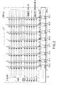
- FIG. 2 shows a detailed configuration by taking out one memory cell array 12 (memory cell array A) and one column control circuit 15 corresponding thereto.
- This memory cell array 12 uses the array of the NAND type memory cell unit formed in the same well CWELLa.
- the NAND type memory cell unit for example, four cell transistors M, each having a shape that the floating gate and the control gate are accumulated, are connected in series, and select transistors S are connected with the both ends thereof.
- One end of this NAND cell unit is connected with either one of bitline BLa_8j to BLa_8j+7, and another end is connected with common source line SRCa.
- the set of cell transistor M of the same line is called one page, and a consecutive set of four pages is called one block.
- the word line corresponding to four cell transistors M in certain one block is shown by WLa_0 to WLa_3, the select gate line of select transistor S on the part side of the NAND cell unit is shown by SG1a_0, and the select gate line of select transistor S on the edge side besides the NAND cell unit is shown by SG2a_0.
- Column control circuit 15 includes data memory circuit 17 connected with bitline BLa_8j to BLa_8j+7 of memory cell array 12. This data memory circuit 17 is electrically connected with signal line IO_0-7 when it is selected by column address signal CSLa_j, temporarily memorizes the data to write in selected memory cell M, and temporarily memorizes the read data read from selected memory cell M.
- Subscript j of bitline BLa_8j to BLa_8j+7 and column select line CSLa_j is from 0 to 548 in memory cell array 12 of FIG. 2. Therefore, bitlines BLa are from BLa_0 to BLa_4391, and column signals CSLa are from CSLa_0 to CSLa_548.
- Memory cell array B is a similar configuration thereto.
- the level of the bitline voltage becomes "L” and "11” can be read.
- "10” can be read by setting the selected word line to 0.9V and "01” and "00” can be read by setting the selected word line to 1.8V.
- Table 2 shows the voltage relation of each operation of the selected block. ERASE WRITE READ BITLINE BL 20V VCC/0V H/L SELECT GATE LINE SG1 20V VCC 4V SELECTED WORD LINE WL 0V 20V 0.0V/0.9V/1.8V UNSELECTED WORD LINE WL - - 10V 4V SELECT GATE LINE SG2 20V 0V 4V SOURCE LINE SRC 20V VCC 0V WELL CWELL 20V 0V 0V
- the page is a physical unit, which shows the set of 4392 memory cells M of the same line shown in FIG. 2, and the logical writing and reading unit are the memory sectors in 4392-bits.
- the data of two logical memory sectors are written on one physical page, or, the data of two logical memory sectors is read from one physical page. That is, an address of the memory sector is specified by row address data Addx_0 to AddX_12 and row address data AddZ. Therefore, a physical unit to be erases is a block, is constructed by four physical pages, and is constructed by eight logical memory sectors.
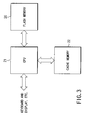
- FIG. 3 is configuration figure of the system to which the flash memory of the configuration shown in FIG. 1 is used.
- Flash memory 20 is controlled with CPU 21 (central processing unit).
- CPU 21 controls cache memory 22, in addition, keyboard, and the display, etc.
- Power-supply voltage VCC is commonly supplied to flash memory 20, CPU 21, and cache memory 22.
- Flash memory 20 automatically reads the data of the predetermined address at the time of raising power-supply voltage VCC by the turning on power supply of this system.
- CPU 21 reads data from flash memory 20 at the time of raising the power supply, and this read data has a code to control flash memory 20.
- CPU 12 stores the above-mentioned code in cache memory 22, controls flash memory 20, reads the program which controls the entire system, and controls the system. Since flash memory 20 automatically performs the error correction, CPU 21 only has to read data from flash memory 20. Though CPU 21 must perform an error correction if flash memory 20 cannot be automatically performed at error correction, since the code to control flash memory 20 is stored in flash memory 20, error correction can not be performed by using only this code.
- FIG. 4 shows the part (check data generation circuit), which generates the check data from the information data (write data, which is the external input) in error correction circuit 11 of the FIG. 1.
- This circuit is chiefly constructed by twenty-one shift registers 18 and nine logical operation circuits 19 shown by D0 to D19 and P.
- FIG. 5A shows the configuration by taking out one shift register 18 (shown by D) in FIG. 4.
- This shift register is driven by complementary signals which consist of clock signal ⁇ and inversion signal n ⁇ thereof, and outputs the latch data by changing the clock signal ⁇ as "L” ⁇ "H” ⁇ “L” (for one cycle of clock signal ⁇ ), and takes and latches the input signal.
- This clock signal ⁇ is a signal which synchronizes with check data generation control signal CGCLK and input control signal INCLK.
- FIG. 5B shows the configuration of one logical operation circuit 19 of the FIG. 4.
- This logical operation circuit performs arithmetic of two input IN1 and IN2 and outputs OUT.
- the logic of the write data input from D0 terminal to D7 terminal is reversed in data I/O buffer 5 and the reversed data is output to signal lines DL_0 to DL_7.
- the check data generation circuit of FIG. 4 is provided to the error correction circuit of the FIG. 1 corresponding to this each signal line DL_0 to DL_7.
- the clock signal ⁇ is turned by one cycle, the write data of one bit is taken into the check data generation circuit of FIG. 4, and the check data with twenty bits is generated in shift register 18 shown by D0 to D19 after 528 cycles of the clock signal ⁇ .
- the parity data is generated in shift register 18 shown by P.
- the check data generated in shift register 18 shown by D0 to D19 are generated in each signal line DL_0 to DL_7 by one bit every time of one cycle of the clock signal ⁇ , switch SW3 is turned on.
- the parity data with one bit is generated in each signal line DL_0 to DL_7. Therefore, the check data with twenty bits and the parity data with one bit are generated from the data with 528 bits input to D0 terminal to D7 terminal by turning the clock signal ⁇ by 549 cycles.
- the check data and the parity data generated like this are output to signal lines DL_0 to DL_7, sent to data memory circuit 17 of the column control circuit 15 shown in FIG. 2, and written in the memory sector selected with the write data.
- FIG. 6 shows the algorithm of the generation of the check data and the parity data in error correction circuit 11 of the FIG. 1.
- the hexadecimal code "80"H is input to command interface 3 as a data input instruction (command) (step S1).
- the address data is input to address buffer 4 and the input of the write data is started (step S2).
- Data input start column addresses AddY_init_0 to AddY_init_9 are input in variable column address register Add_col in column address generation circuit 16, and column address signal CSL is generated according to the content of this variable column address register Add_col (step S3).
- step S4 The registers shown by D0 to D19 and P are reset to "0" and the write data to data memory circuit 17 is reset to "1" (step S4).
- Switch SW1 is turned on, and switch SW3 and SW5 are turned off (step S5).
- step S6 the write data input to D0 terminal to D7 terminal are taken (step S6).
- Switch SW2 and SW4 are turned off (step S9) if it is judged that the content of variable column address register Add_col is 516 (step S7), and switch SW2 and SW4 are turned on if it is judged that the content of variable column address register Add_col is not 516 (step S8).
- step S10 the write data is taken into error correction circuit 11 and the check data and the parity data are calculated (step S10). That is, the clock signal ⁇ is turned by one cycle. At this time, column address signal CSL is output and the write data is also memorized in data memory circuit 17. And, the content of variable column address register Add_col is incremented by one, and the write data is taken in order of the column address (step S11). Operations of steps S6 to S12 are repeated until input of, for example, the hexadecimal code "10"H, which is the write instruction, is judged (step S12).
- steps S6 to S12 are performed in synchronization with write enable signal nWE.
- Input control signal INCLK is generated by input control signal generation circuit 10 in synchronization with write enable signal nWE.
- the write data input in synchronization with write enable signal nWE is taken into error correction circuit 11 according to the clock signal ⁇ generated by error correction circuit 11 in synchronization with input control signal INCLK, and temporarily memorized in data memory circuit 17 selected at the same time with the instruction of column address signal CSL generated in synchronization with input control signal INCLK according to the content of variable column address register Add_col.
- step S12 When the input of the hexadecimal code "10"H, which is the write instruction, is judged in step S12, whether the content of variable column address register Add_col is larger than that of 527 (step S13) is judged. As a result of this judgment, if the content of variable column address register Add_col is equal to or smaller than 527, switches SW2 and SW4 are turned off (step S14), the check data and parity are calculated, it is assumed that "1" write data is input virtually (step S15), the content of variable column address register Add_col is incremented by one (step S16), and whether the content of variable column address register Add_col is larger again than that of 527 (step S13) is judged, again.
- step S17 if the content of variable column address register Add_col is equal to or smaller than 528, it is further judged whether the content of variable column address register Add_col is 548 (step S17). As a result of this judgment, if the content of variable column address register Add_col is not equal to 548, switch SW1 and SW5 are turned off and switch SW3 and SW4 are turned on (step S18), and parity arithmetic is performed with the output of the check data (step S19). At this time, the check data is temporarily memorized in data memory circuit 17 according to the content of variable column address register Add_col. And, the content of variable column address register Add_col is incremented by one (step S20), and whether content of variable column address register Add_col is equal to 548 or not is judged again (step S17).
- step S21 when the content of variable column address register Add_col becomes 548, switch SW3 is turned off and switch SW5 is turned on (step S21), and the parity data is output (step S22).
- step S21 when the content of variable column address register Add_col becomes 548, switch SW3 is turned off and switch SW5 is turned on (step S21), and the parity data is output (step S22).
- step S21 the check data is temporarily memorized in data memory circuit 17 according to the content of variable column address register Add_col.
- the write data, the check data, and the parity data memorized in data memory circuit 17 are basically written in the memory sector in a lump (step S23).
- Step S13 to S22 are performed in synchronization with check data generation control signal CGCLK.
- Check data generation instruction CHKGEN is generated by write instruction signal PRO, and check data generation control signal CGCLK is automatically generated in check data generation control signal generation circuit 9 by this check data generation instruction CHKGEN.
- the check data and the parity data generated from error correction circuit 11 in synchronization with this check data generation control signal CGCLK is temporarily memorized to data memory circuit 17 selected by the instruction of column address signal CSL generated according to the content of variable column address register Add_col in synchronization with check data generation control signal CGCLK at the same time.
- FIG. 7 shows an example of the timing of operation to select the memory sector from each array A and B in memory cell array 12 one by one and to write data in two sectors at the same time.
- FIG. 8 shows an example of the timing of operation to select the memory sector from each array A and B in memory cell array 12 one by one and to write data in only sector.
- the address data is taken thrice in the period when address latch enable signal ALE is "H", as described in steps S2 to S5 of FIG. 6.
- the address in cell array A in memory cell array 12 is input.
- Data input instruction signal INPUT becomes "H” and write data h0 to h527 are input as described in steps S6 to S12 of FIG. 6.
- Write data h is input in synchronization with write enable signal nWE, is taken into error correction circuit 11 according to the clock signal ⁇ generated by error correction circuit 11 in synchronization with input control signal INCLK, and is temporarily memorized in data memory circuit 17 selected by the instruction of column address signal CSL generated at the same time, in synchronization with INCLK according to the content of variable column address register Add_col.
- check data generation control signal CGCLK is generated by this check data generation instruction signal CHKGEN, and the check data and the parity data generated from error correction circuit 11 in synchronization with this check data generation control signal CGCLK are temporarily memorized in data memory circuit 17 selected at the same time by the instruction of column address signal CSL generated in synchronization with CGCLK according to the content of variable column address register Add_col.
- step S23 of FIG. 6 The writing operation of an effective writing (step S23 of FIG. 6) is not performed by the hexadecimal code "D0"H, which is the double-speed write instruction, when the parity data is memorized in data memory circuit 17, write instruction signal PRO and check data generation instruction signal CHKGEN become “L", and write is ended. nBUSY becomes “L” and the busy state (during internal processing) is informed to the external device in the period when write instruction signal PRO and check data generation instruction signal CHKGEN are "H".
- the hexadecimal code "80"H which is the data input instruction, is input at raise of write enable signal nWE in the period when command latch enable signal CLE is "H", as described in step S1 of FIG. 6.
- the address data is taken thrice in the period when address latch enable signal ALE is "H", as described in steps S2 to S5 of FIG. 6.
- the address in cell array B in memory cell array 12 is input.
- write data h is input in synchronization with write enable signal nWE, is taken into error correction circuit 11 according to the clock signal ⁇ generated in synchronization with INCLK in error correction circuit 11, and is temporarily memorizes to data memory circuit 17 selected by the instruction of column address signal CSL generated in synchronization with input control signal INCLK according to the content of variable column address register Add_col at the same time.
- write data h0 to h2 are not input, but the write data of data memory circuit 17 is reset to "1", if write data h0 to h2 are "1" in the error correction circuit 11, there is no disadvantage since the contents of the register shown by D0 to D19 and the register shown by P do not change by the arithmetic to h2. That is, write data h0 to h2 are assumed to be "1" in the effect.
- write instruction signal PRO becomes “H", as described in steps S13 to S22 of FIG. 6, and check data generation instruction signal CHKGEN becomes “H” by this write instruction signal PRO, too.
- Check data generation control signal CGCLK is generated by this check data generation instruction signal CHKGEN, and the dummy write data "1" is generated internally in synchronization with CGCLK instead of write data h521 to h527, which are not input from the external device.
- the check data and the parity data generated from error correction circuit 11 in synchronization with above-mentioned check data generation control signal CGCLK are temporarily memorized to data memory circuit 17 selected by the instruction of column address signal CSL generated in synchronization with CGCLK according to the content of variable column address register Add_col at the same time.
- check data generation instruction signal CHKGEN becomes "L"
- write operation is started.
- writing is performed to two memory sectors selected from cell arrays A and B of memory cell array 12 at the same time.
- nBUSY becomes “L” and the busy state (internal processing) is informed to the external device in the period when write instruction signal PRO is "H”.
- FIG. 9 shows an example of the timing of the data writing operation when error correction circuit 11 is deactivated.
- the hexadecimal code "A0"H is input, for example, as an error correction deactivation instruction at of raise of write enable signal nWE in the period when command latch enable signal CLE “H".
- the hexadecimal code "80"H is input as a data input instruction at raise of command latch enable signal CLE in the period when write enable signal nWE is "H".
- Address latch and enable signal ALE are continuously taken and the address data is taken thrice in the period of "H".
- Data input instruction signal INPUT continuously becomes “H”, and write data h0 to h548 are input. If the hexadecimal code "10"H, which is the write instruction, is input, though write instruction signal PRO becomes “H”, check data generation instruction signal CHKGEN is "L”. It immediately becomes in write operation after the hexadecimal code "10", which is the write instruction, is input.
- Command interface 3 switches whether error correction circuit 11 is activated or deactivated.
- error correction circuit activation signal ECCENB input to the terminal ECCENB is assumed to be "L”
- command interface 3 is switched to deactivate error correction circuit 11.
- FIG. 10 shows an example of the timing of the data writing operation when error correction circuit activation signal ECCENB is assumed to be "L".
- the hexadecimal code "A0"H as the error correction deactivation instruction is input at raise of write enable signal nWE in the period when command latch enable signal CLE is “H”. Continuously the address data is taken thrice in the period when address latch and enable signal ALE are “H”.
- Data input instruction signal INPUT becomes “H”
- write data h0 to h548 are input. If the hexadecimal code "10"H, which is the write instruction, is input, write instruction signal PRO becomes “H”, but check data generation instruction signal CHKGEN is “L”. It immediately becomes in write operation after the hexadecimal code "10", which is the write instruction, is input.
- Error correction circuit activation signal ECCENB shows "H” at the operation timing shown in FIG. 8, and the check data is automatically generated by the flow of the data input instruction "80" ⁇ address input ⁇ data input ⁇ write instruction "10", as well as the operation timing shown in FIG. 10.
- error correction circuit activation signal ECCENB shows "L”
- the check data is not generated like the operation timing shown in FIG. 10.
- FIG. 11 to FIG. 17 show the part of correcting and detecting data in which the error is caused from the data read from the memory cell in error correction circuit 11 of the FIG. 1.
- FIG. 11 shows one syndrome S1 and S3 calculator
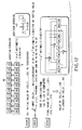
- FIG. 12 shows one converter of syndrome S3
- FIG. 15 shows one ⁇ 1 ⁇ ⁇ 1 converter
- FIG. 16 shows one ⁇ 2 ⁇ ⁇ 2 converter
- FIG. 17 shows one error position detector.
- These circuits are chiefly constructed by 51 shift registers 18 shown by D0 to D19, P, A0 to A9, B0 to B9, and C0 to C9 and a plurality of logical operation circuits 19, and provided respectively corresponding to each signal line DL_0 to DL_7.
- Syndrome S1 and S3 calculator shown in FIG. 11 is, chiefly, constructed by 31 shift registers 18 shown by D0 to D19, P, and A0 to A9, and a plurality of logical operation circuits 19.
- Logic of the read data read from the memory sector to data memory circuit 17 is reversed in IO buffer 6 and reversed data is output to signal lines DL_0 to DL_7.
- Column address signal CSL is generated in synchronization with error correction control signal ECCLK, the read data in 0 column addresses is taken into the first cycle of the clock signal ⁇ , hereinafter, sequentially, the read data in one column address in the second cycle, ... , the read data in 547th column address is taken into the 548th cycle.
- Switches SW4, SW6, and SW7 become turned off, and the dummy data "0" is taken at the cycle in 516th column address.
- the reason is write data of 516th address is calculated as the dummy data "0" when the check data is generated.
- Syndrome S1 is memorized in the registers shown by A0 to A9.
- syndrome S1 is memorized in the registers shown by D0 to D9
- syndrome S3 is memorized in the registers shown by D10 to D19
- syndrome S1 is memorized in the registers shown by A0 to A9
- the parity of the read data is memorized in the register shown by P.
- syndrome S3 obtained with syndrome S1 and S3 calculator shown in FIG. 11 is different the degree of the polynomial expression from syndrome S1, it is matched by the converter of syndrome S3 shown in FIG. 12.
- the converter of syndrome S3 shown in FIG. 12 is chiefly constructed by 20 shift registers 18 shown by B0 to B9 and C0 to C9 and a plurality of logical operation circuits 19, and syndrome S3 is matched to syndrome S1.
- syndrome S1 is memorized in the registers shown by D0 to D9
- syndrome S3 is memorized in the registers shown by D10 to D19
- syndrome S1 is memorized in the registers shown by A0 to A9
- the parity of the read data is memorized in the register shown by P.
- the calculator of syndrome S1 ⁇ S1 shown in FIG. 13 is chiefly constructed by 20 shift registers 18 shown by B0 to B9 and C0 to C9 and a plurality of logical operation circuits 19, and calculates syndrome S1 ⁇ S1.
- S1 ⁇ S1 is caused in the register shown by C in STEP1. This is memorized in the registers shown by D0 to D9.
- the calculator of syndrome S1 ⁇ S1 ⁇ S1 + S3 shown in FIG. 14 is chiefly constructed by 20 shift registers 18 shown by B0 to B9 and C0 to C9 and a plurality of logical operation circuits 19, and calculates syndrome S1 ⁇ S1 ⁇ S1 + S3.
- the error position detector can operate by using ⁇ 1 obtained with the calculator of syndrome S1 ⁇ S1 ⁇ S1 + S3 shown in FIG. 14, since it takes time to access, ⁇ 1 is converted into ⁇ 1 with the ⁇ 1 ⁇ ⁇ 1 converter shown in FIG. 15 to perform the access at high speed.
- the ⁇ 1 ⁇ ⁇ 1 converter shown in FIG. 15 is chiefly constructed by 20 shift registers 18 shown by B0 to B9 and C0 to C9 and a plurality of logical operation circuits 19, and converts ⁇ 1 into ⁇ 1.
- ⁇ 1 is memorized in the registers shown by D0 to D9
- ⁇ 2 is memorized in the registers shown by D10 to D19
- syndrome S1 is memorized in the registers shown by A0 to A9
- the parity of the read data is memorized in the register shown by P.
- the error position detector can operate even like ⁇ 2 obtained with the ⁇ 1 ⁇ ⁇ 1 converter shown in FIG. 15, since it takes time to access, ⁇ 2 is converted into ⁇ 2 with the ⁇ 2 ⁇ ⁇ 2 converter shown in FIG. 16 to perform the access at high speed.
- the ⁇ 2 ⁇ ⁇ 2 converter shown in FIG. 16 is chiefly constructed by 20 shift registers 18 shown by B0 to B9 and C0 to C9 and a plurality of logical operation circuits 19, and converts ⁇ 2 into ⁇ 2.
- ⁇ 1 is memorized in the registers shown by D0 to D9
- ⁇ 2 is memorized in the registers shown by D10 to D19
- syndrome S1 is memorized in the registers shown by A0 to A9
- the parity of the read data is memorized in the register shown by P.
- the error position detector shown in FIG. 17 is chiefly constructed by 30 shift registers 18 shown by D0 to D19, A0 to A9, and a plurality of logical operation circuits 19.
- This error position detector detects the error position by using syndrome ⁇ 1 memorized in the register shown by D0 to D9, ⁇ 2 memorized in the register shown by D10 to D19, and S1 memorized in the registers shown by A0 to A9, and operates by the clock signal ⁇ generated in synchronization with output control signal OUTCLK generated in output control signal generation circuit 8.
- the read data in 0 column address is erroneous.
- FIG. 18 shows an example of the algorithm, in which the error position detection and correction is performed from the read data with error correction circuit 11 of the FIG. 1.
- step S101 the memory sector and start column address data, to which reading are started, are input (step S101).
- step S102 data is read from the memory sector to data memory circuit 17 (step S102).
- step S103 the register shown by D0 to D19 and the register shown by P are reset to "0" (step S103).
- step S104 the content of variable column address register Add_col is set to 0 (step S104).
- This variable column address register Add_col is in column address generation circuit 16, and generates column address signal CSL according to the content of this variable column address register Add_col.
- the read data is output from the data memory circuit 17 selected by the column address (step S105). And, it is judged whether the content of variable column address register Add_col is 516 (step S106), switch SW4, SW6, and SW7 are turned off (step S108), when the content of variable column address register Add_col is 516, switch SW4, SW6, and SW7 are turned on if the content of variable column address register Add_col is not 516 (step S107).
- step S109 arithmetic of the syndrome and parity is performed by the clock signal ⁇ generated in synchronization with error correction control signal ECCLK. And, it is judged the content of variable column address register Add_col is equal to 547 (step S110), and process is moved to step S111 if it is not 547, and the content of variable column address register Add_col is advanced by one and flowchart is returned to step S105. Thus, the arithmetic of the syndrome and parity is repeated while incrementing it by one until the content of variable column address register Add_col becomes equal to 547. Above-mentioned operations of steps S105 to S111 are performed in synchronization with error correction control signal ECCLK.
- step S118 it is judged whether the parity generated from the write data is coincide with the parity generated from the read data (step S120). As a result of this judgment, if parities are coincide, it is judged the error by two bits is caused, and "TWO BITS ERROR” is set in status (step S121). As a result of this judgment in step S120, if parities are not coincide, it is judged that the error in three bits or more is caused, and "INCORRECTABLE" is set in status (step S122). And, when status is fixed, the content of variable column address register Add_col is set to 0 again (step S123). The operations of above-mentioned steps S112 to S123 and S105 to S111 are performed in synchronization with error correction control signal ECCLK.
- step S124 the error position arithmetic is performed in one cycle (step S124), and it is judged whether the content of variable column address register Add_col is coincide with the column address of the data output start (step S125). As a result of this judgment, process is moved to step S126 if not coincide, and content of variable column address register Add_col is advanced by one, and flowchart is returned to step S124. Thus, the content of variable column address register Add_col is incremented by one until it is coincide with the column address of the data output start, and steps S124 to S126 are repeated. Operations of above-mentioned steps S124 to S126 is performed in synchronization with the clock signal ⁇ generated in synchronization with error correction control signal ECCLK.
- variable column address register Add_col If it is judged that the content of variable column address register Add_col is coincide with the column address of the data output start by step S125, the error position arithmetic is performed in synchronization with OUTCLK generated in synchronization with read enable signal nRE, and data is output to the external device according to the content of variable column address register Add_col (step S127).
- the error position arithmetic and data output are repeated requested times from the external device by read enable signal nRE. It is possible to output at high speed by examining whether it is necessary to correct output data like this in a previous cycle. Output processing and judging processing to be corrected may be performed at the same cycle when the high-speed output is not required.
- FIG. 19 shows an example of the timing of the data read operation in the algorithm shown in FIG. 18.
- address data ad0 to ad2 which specify the selection of the memory sector and the data output start column address, are input at raise of write enable signal nWE in the period when address latch enable signal ALE is "H", (step S101 of FIG. 18).
- read instruction signal READ automatically becomes “H", and the data of the memory cell is read from the selected memory sector to data memory circuit 17 (step S102 of FIG. 18).
- the registers shown by D0 to D19 and the register shown by P are reset to "0" meanwhile (step S103 of FIG. 18), and the content of variable column address register Add_col is set to 0(step S104 of FIG. 18).
- variable column address register Add_col is in column address generation circuit 16, and column address signal CSL is generated according to the content of this variable column address register Add_col.
- data latch read instruction signal DLREAD becomes "H"
- error correction control signal ECCLK is output.
- the read data is sequentially output from the data memory circuit 17 selected by the column address to error correction circuit 11 from 0th column address to 547th column address in synchronization with error correction control signal ECCLK, and the calculation of the syndrome and parity is performed (steps S105 to S111 of FIG. 18).
- calculation instruction signal CALC becomes "H"
- error correction control signal ECCLK is output again.
- the error detection of the read data is performed in synchronization with error correction control signal ECCLK (steps S112 to S122 of FIG. 18).
- Data output instruction signal OUTPUT becomes "H” when CALC becomes “L”, output control signal OUTCLK is output, and the output preparation to the external device is performed (steps S123 to S126 of FIG. 18). Since the data output start column address is "1" address in the example of FIG. 19, the error position arithmetic (step S124 of FIG. 18) is performed twice.
- read instruction signal READ becomes “L”
- the output to the external device becomes possible.
- Busy signal nBUSY is "L”
- preparation of the output to the external device is informed when read instruction signal READ is "H”.
- Output control signal OUTCLK becomes from “L” to “H” according to the timing that read enable signal nRE changes from “H” to “L”, column address signal CSL is output, and the output is started from D0 terminal to D7 terminal corresponding to read data D0 to D7.
- the error position arithmetic is performed to detect whether the output data of the following column address has an error (step S127 of FIG. 18).
- 0 is output if succeeding and 1 is output if not succeeding.
- the status data of the register shown by D0 is made common as status data of reading/writing/the erasure.
- the register shown by D1 and the register shown by D2 show the maximum number of errors.
- the circuits of FIG. 11 to FIG. 17 are provided corresponding to each of signal lines DL_0 to DL_7, and the number of errors can be obtained therefrom since they operate at the same time.
- the maximum number of errors is output as status.
- FIG. 20 shows an example of the timing of operation, which output the read data without performing the error correction in the algorithm shown in FIG. 18.
- the check data and the parity data are output.
- the operation of error correction circuit 11 can be checked by the external device.
- the hexadecimal code "B0"H which is the error correction deactivation instruction, is input at raise of write enable signal nWE in the period when command latch enable signal CLE is "H".
- the same command as the error correction deactivation instruction "A0"H at the time of writing may be used as this error correction deactivation instruction.
- the timing of the operation shown in FIG. 20 is almost the same as the timing of the operation shown in FIG. 19. The difference is that (1) "B0"H command is entered, (2) output data without correction even when the error data is detected, and (3) the check data and the parity data are output.
- FIG. 21 shows an example of the timing of the data read operation when error correction circuit activation signal ECCENB input to the terminal ECCENB is set to "L".
- error correction circuit activation signal ECCENB is "L"
- command interface 3 in FIG. 1 switches to deactivate error correction circuit 11.
- address data ad0 to ad2 which specify the selection of the memory sector and the data output start column address, are input at raise of write enable signal nWE in the period when address latch enable signal ALE is "H".
- Read instruction signal READ automatically becomes “H” when address data ad2 is taken, and the data of the memory cell is read from the selected memory sector to data memory circuit 17. Thereafter, read instruction signal READ becomes “L”, and the output to the external device becomes enabled. Data output instruction signal OUTPUT becomes “H”, and the output of output control signal OUTCLK becomes possible. Preparing the output to the external device is informed, by making busy signal nBUSY is “L”, and preparation of the output to the external device is informed when read instruction signal READ is "H”.
- FIG. 22 shows an example of the timing of operation, which automatically reads the memory sector of a predetermined address in the system, which shows in FIG. 3 at the time of raise of the power supply.
- the timing of the operation shown in FIG. 22 is almost the same as the timing of the operation shown in FIG. 19, the difference is to be started by power on detection signal PON.
- the second embodiment differs from the first embodiment only in read operation.
- the circuit configuration of the flash memory, which equips the error correction circuit, according to the second embodiment is almost similar to the circuit configuration shown in FIG. 1, and, in addition, the point to receive the error correction instruction from the external device and output error correction read instruction signal ECREAD from the command interface 3 is different.
- FIG. 23 shows an example of algorithm, which performs the error position detection and correction from the read data with error correction circuit 11 of the FIG. 1, in the second embodiment, and differs from the algorithm, which performs the error position detection and correction from the read data with error correction circuit 11 of the FIG. 1, in the first embodiment referring to FIG. 18.
- step S201 the memory sector and the start column address data, which starts reading, is input (step S201).
- step S202 data is read from the memory sector to data memory circuit 17 (step S202).
- step S203 the registers shown by D0 to D19 and the register shown by P are reset to "0" (step S203).
- step S204 the content of variable column address register Add_col is set to 0 (step S204). This variable column address register Add_col is in column address generation circuit 16, and column address signal CSL is generated according to this content.
- step S205 the read data from the data memory circuit 17 selected by the column address is output to the external device (step S205). And, it is judged whether the content of variable column address register Add_col is 516 or not (step S206), switches SW4, SW6, and SW7 are turned off (step S208) if the content is 516, and switches SW4, SW6, and SW7 are turned on if the content is not 516 (step S207).
- step S209 arithmetic of the syndrome and parity is performed (step S209) by the clock signal ⁇ generated in synchronization with output control signal OUTCLK, which synchronizes with read enable signal nRE from the external device.
- step S210 the content of variable column address register Add_col is advanced by one and flowchart is returned to step S205 (step S210).
- step S210 the arithmetic of the syndrome and parity is repeated while incrementing by one, until the content of variable column address register Add_col becomes 527. Operations of above-mentioned steps S205 to S210 are performed in synchronization with output control signal OUTCLK.
- step S211 if the hexadecimal code "20"H is input to command interface 3, for example, as an error read instruction, it becomes error correction operation by correction read instruction signal ECREAD (step S211). And, switch SW4, SW6, and SW7 are turned on (step S212). In addition, arithmetic of the syndrome and parity is performed (step S213) by the clock signal ⁇ generated in synchronization with error correction control signal ECCLK.
- step S214 It is judged whether the content of variable column address register Add_col is 547 (step S214), and process is moved to step S215, then, the content is incremented by one, and flowchart is returned to step S213 if the content is not 547. Thus, the arithmetic of the syndrome and parity is repeated while incrementing by one, until the content of variable column address register Add_col becomes 547.
- steps S213 to S215 and S105 to S111 are performed in synchronization with error correction control signal ECCLK.
- step S224 it is judged whether the parity generated from the write data is coincide with the parity generated from the read data. As a result of this judgment, if parities are coincide, it is judged the error by two bits is caused, and "TWO BITS ERROR" is set in status (step S225).
- step S224 if parities are not coincide, it is judged that the error in three bits or more is caused, and "INCORRECTABLE" is set in status (step S226). And, when status is fixed, the content of variable column address register Add_col is set to 0 again (step S227).
- the operations of above-mentioned steps S216 to S228 are performed in synchronization with error correction control signal ECCLK.
- step S230 When the hexadecimal code "70"H, which is the status read instruction, is input at raise of write enable signal nWE in the period when command latch enable signal CLE is "H" (step S229), the status set as described in steps S218, S219, S223, S225, and S226 is output (step S230).
- status read instruction signal STATUS When the status read instruction "70”H is input, status read instruction signal STATUS becomes “H”. That is, if the status read instruction "70”H is input, status read instruction signal STATUS becomes “H”.
- FIG. 24 shows an example of the timing of the data read operation in the algorithm shown in FIG. 23.
- Address data ad0 to ad2 which specify the selection of the memory sector and the data output start column address, are input at raise of write enable signal nWE in the period when address latch enable signal ALE is "H" (step S201 of FIG. 23).
- Read instruction signal READ automatically becomes “H” when address data ad2 is taken, and the data of the memory cell is read from the selected memory sector to data memory circuit 17 (step S202 of FIG. 23).
- the registers shown by D0 to D19 and the register shown by P are reset to "0" meanwhile (step S203 of FIG. 23), and the content of variable column address register Add_col is set to 0 (step S204 of FIG. 23).
- This variable column address register Add_col is in column address generation circuit 16, and column address signal CSL is generated according to this content.
- Busy signal nBUSY is "L", and preparation of the output to the external device is informed when read instruction signal READ is "H".
- error correction read instruction signal ECREAD becomes “H"
- data latch read instruction signal DLREAD becomes “H”
- ECCLK error correction control signal
- the read data is sequentially output from the data memory circuit 17 selected by the column address to error correction circuit 11 from 528th column address to 547th column address in synchronization with error correction control signal ECCLK, and the calculation of the syndrome and parity is performed (steps S212 to S215 of FIG. 23).
- calculation instruction signal CALC becomes "H"
- error correction control signal ECCLK is output again.
- the error detection of the read data is performed in synchronization with error correction control signal ECCLK (steps S216 to S226 of FIG. 23).
- output control signal OUTCLK becomes from “L” to “H” according to the timing that read enable signal nRE change from “H” to “L”
- column address signal CSL is output, and the output of the read data is started from D0 terminal to D7 terminal.
- the error position arithmetic is performed to detect whether the output data of the following column address has an error. It is possible to output at high speed by examining whether it is necessary to correct output data like this in a previous cycle. Output processing and judging processing to be corrected may be performed at the same cycle when the high-speed output is not required.
- the second above-mentioned embodiment it can facilitate to activate and deactivate the error correction circuit as described in the first embodiment. It can facilitate the output of the check data and the parity data.
- FIG. 25 shows an example of the timing of the data erase operation in the flash memory according to the first embodiment and the second embodiment.
- the parity data is one of the check data to check the level of the error.
Landscapes
- Engineering & Computer Science (AREA)
- Theoretical Computer Science (AREA)
- Quality & Reliability (AREA)
- Physics & Mathematics (AREA)
- General Engineering & Computer Science (AREA)
- General Physics & Mathematics (AREA)
- Microelectronics & Electronic Packaging (AREA)
- Read Only Memory (AREA)
- For Increasing The Reliability Of Semiconductor Memories (AREA)
- Techniques For Improving Reliability Of Storages (AREA)
Applications Claiming Priority (3)
| Application Number | Priority Date | Filing Date | Title |
|---|---|---|---|
| JP18187499 | 1999-06-28 | ||
| JP18187499A JP4074029B2 (ja) | 1999-06-28 | 1999-06-28 | フラッシュメモリ |
| EP00113125A EP1065594B1 (fr) | 1999-06-28 | 2000-06-28 | Circuit de détection et de correction d'erreur dans une mémoire flash |
Related Parent Applications (1)
| Application Number | Title | Priority Date | Filing Date |
|---|---|---|---|
| EP00113125A Division EP1065594B1 (fr) | 1999-06-28 | 2000-06-28 | Circuit de détection et de correction d'erreur dans une mémoire flash |
Publications (3)
| Publication Number | Publication Date |
|---|---|
| EP1450259A2 true EP1450259A2 (fr) | 2004-08-25 |
| EP1450259A3 EP1450259A3 (fr) | 2004-10-20 |
| EP1450259B1 EP1450259B1 (fr) | 2007-08-01 |
Family
ID=16108377
Family Applications (2)
| Application Number | Title | Priority Date | Filing Date |
|---|---|---|---|
| EP04011269A Expired - Lifetime EP1450259B1 (fr) | 1999-06-28 | 2000-06-28 | Mémoire flash |
| EP00113125A Expired - Lifetime EP1065594B1 (fr) | 1999-06-28 | 2000-06-28 | Circuit de détection et de correction d'erreur dans une mémoire flash |
Family Applications After (1)
| Application Number | Title | Priority Date | Filing Date |
|---|---|---|---|
| EP00113125A Expired - Lifetime EP1065594B1 (fr) | 1999-06-28 | 2000-06-28 | Circuit de détection et de correction d'erreur dans une mémoire flash |
Country Status (7)
| Country | Link |
|---|---|
| US (6) | US6611938B1 (fr) |
| EP (2) | EP1450259B1 (fr) |
| JP (1) | JP4074029B2 (fr) |
| KR (1) | KR100378272B1 (fr) |
| CN (2) | CN1206657C (fr) |
| DE (2) | DE60013044T2 (fr) |
| TW (1) | TW473719B (fr) |
Cited By (1)
| Publication number | Priority date | Publication date | Assignee | Title |
|---|---|---|---|---|
| CN107918571A (zh) * | 2016-10-08 | 2018-04-17 | 上海宝存信息科技有限公司 | 测试储存单元的方法以及使用该方法的装置 |
Families Citing this family (116)
| Publication number | Priority date | Publication date | Assignee | Title |
|---|---|---|---|---|
| JP4112849B2 (ja) | 2001-11-21 | 2008-07-02 | 株式会社東芝 | 半導体記憶装置 |
| JP3851865B2 (ja) | 2001-12-19 | 2006-11-29 | 株式会社東芝 | 半導体集積回路 |
| CN1319071C (zh) * | 2002-08-07 | 2007-05-30 | 飞虹积体电路股份有限公司 | 以快闪存储器模拟电擦除可编程只读存储器的系统及方法 |
| JP4129381B2 (ja) | 2002-09-25 | 2008-08-06 | 株式会社ルネサステクノロジ | 不揮発性半導体記憶装置 |
| US7296213B2 (en) * | 2002-12-11 | 2007-11-13 | Nvidia Corporation | Error correction cache for flash memory |
| JP4314057B2 (ja) | 2003-04-18 | 2009-08-12 | サンディスク コーポレイション | 不揮発性半導体記憶装置および電子装置 |
| ITRM20030198A1 (it) * | 2003-04-28 | 2004-10-29 | Micron Technology Inc | Monitor ad unita' di controllo basata su rom in un |
| US7703780B2 (en) * | 2003-09-30 | 2010-04-27 | Toyota Jidosha Kabushiki Kaisha | Wheel supporting apparatus improving ride comfort of vehicle |
| US7012835B2 (en) * | 2003-10-03 | 2006-03-14 | Sandisk Corporation | Flash memory data correction and scrub techniques |
| US7865809B1 (en) | 2004-03-11 | 2011-01-04 | Super Talent Electronics, Inc. | Data error detection and correction in non-volatile memory devices |
| JP2005327437A (ja) * | 2004-04-12 | 2005-11-24 | Nec Electronics Corp | 半導体記憶装置 |
| US7882299B2 (en) * | 2004-12-21 | 2011-02-01 | Sandisk Corporation | System and method for use of on-chip non-volatile memory write cache |
| US7844879B2 (en) | 2006-01-20 | 2010-11-30 | Marvell World Trade Ltd. | Method and system for error correction in flash memory |
| US8055979B2 (en) * | 2006-01-20 | 2011-11-08 | Marvell World Trade Ltd. | Flash memory with coding and signal processing |
| JP4846384B2 (ja) * | 2006-02-20 | 2011-12-28 | 株式会社東芝 | 半導体記憶装置 |
| JP4836608B2 (ja) * | 2006-02-27 | 2011-12-14 | 株式会社東芝 | 半導体記憶装置 |
| DE602006006788D1 (de) * | 2006-03-02 | 2009-06-25 | St Microelectronics Srl | Leseverfahren eines Speichers mit eingebetteter Fehlerkorrekturkode und Speicher mit eingebetteter Fehlerkorrekturkode |
| JP2007305267A (ja) * | 2006-05-15 | 2007-11-22 | Toshiba Corp | 半導体記憶装置 |
| US7624329B2 (en) * | 2006-08-30 | 2009-11-24 | Freescale Semiconductor, Inc. | Programming a memory device having error correction logic |
| US7809899B2 (en) * | 2007-05-29 | 2010-10-05 | Lsi Corporation | System for integrity protection for standard 2n-bit multiple sized memory devices |
| WO2009095902A2 (fr) * | 2008-01-31 | 2009-08-06 | Densbits Technologies Ltd. | Systèmes et procédés pour traiter des erreurs de données immédiates dans une mémoire flash |
| WO2009037697A2 (fr) * | 2007-09-20 | 2009-03-26 | Densbits Technologies Ltd. | Systèmes et procédés améliorés pour déterminer les valeurs logiques de cellules de mémoire flash couplées |
| US8694715B2 (en) | 2007-10-22 | 2014-04-08 | Densbits Technologies Ltd. | Methods for adaptively programming flash memory devices and flash memory systems incorporating same |
| US8443242B2 (en) | 2007-10-25 | 2013-05-14 | Densbits Technologies Ltd. | Systems and methods for multiple coding rates in flash devices |
| WO2009072105A2 (fr) * | 2007-12-05 | 2009-06-11 | Densbits Technologies Ltd. | Recherche de chien de faible puissance basée sur un système de décodage bch/reed-solomon destiné à une mémoire flash, dispositifs de communications mobiles et autres applications |
| US8335977B2 (en) | 2007-12-05 | 2012-12-18 | Densbits Technologies Ltd. | Flash memory apparatus and methods using a plurality of decoding stages including optional use of concatenated BCH codes and/or designation of “first below” cells |
| US8321625B2 (en) | 2007-12-05 | 2012-11-27 | Densbits Technologies Ltd. | Flash memory device with physical cell value deterioration accommodation and methods useful in conjunction therewith |
| WO2009074978A2 (fr) | 2007-12-12 | 2009-06-18 | Densbits Technologies Ltd. | Systèmes et procédés pour une correction d'erreurs et un décodage sur des milieux physiques à multiples niveaux |
| WO2009074979A2 (fr) * | 2007-12-12 | 2009-06-18 | Densbits Technologies Ltd. | Système de recherche de chien employant un schéma de désactivation du signal d'horloge pour économiser de l'énergie pour un décodeur correcteur d'erreurs et autres applications |
| US8327246B2 (en) | 2007-12-18 | 2012-12-04 | Densbits Technologies Ltd. | Apparatus for coding at a plurality of rates in multi-level flash memory systems, and methods useful in conjunction therewith |
| JP4672742B2 (ja) * | 2008-02-27 | 2011-04-20 | 株式会社東芝 | メモリコントローラおよびメモリシステム |
| WO2009118720A2 (fr) * | 2008-03-25 | 2009-10-01 | Densbits Technologies Ltd. | Appareil et procédés pour l’arrondi non biaisé à efficacité matérielle |
| JP2008251154A (ja) * | 2008-04-11 | 2008-10-16 | Renesas Technology Corp | 不揮発性半導体記憶装置 |
| US8332725B2 (en) | 2008-08-20 | 2012-12-11 | Densbits Technologies Ltd. | Reprogramming non volatile memory portions |
| US8458574B2 (en) * | 2009-04-06 | 2013-06-04 | Densbits Technologies Ltd. | Compact chien-search based decoding apparatus and method |
| US8819385B2 (en) | 2009-04-06 | 2014-08-26 | Densbits Technologies Ltd. | Device and method for managing a flash memory |
| CN101872318B (zh) * | 2009-04-22 | 2012-10-24 | 群联电子股份有限公司 | 用于快闪记忆体的资料存取方法及其储存系统与控制器 |
| KR101575248B1 (ko) | 2009-04-30 | 2015-12-07 | 삼성전자주식회사 | 메모리 컨트롤러 및 그것을 포함하는 메모리 시스템 |
| US8566510B2 (en) | 2009-05-12 | 2013-10-22 | Densbits Technologies Ltd. | Systems and method for flash memory management |
| US8225052B2 (en) * | 2009-06-03 | 2012-07-17 | Micron Technology, Inc. | Methods for controlling host memory access with memory devices and systems |
| JP5668279B2 (ja) | 2009-08-06 | 2015-02-12 | ソニー株式会社 | 不揮発性ランダムアクセスメモリおよび不揮発性メモリシステム |
| EP2299362A3 (fr) * | 2009-08-18 | 2011-05-04 | ViaSat, Inc. | Correction d'erreurs sans voie de retour pour mémoires |
| US8305812B2 (en) * | 2009-08-26 | 2012-11-06 | Densbits Technologies Ltd. | Flash memory module and method for programming a page of flash memory cells |
| US8995197B1 (en) | 2009-08-26 | 2015-03-31 | Densbits Technologies Ltd. | System and methods for dynamic erase and program control for flash memory device memories |
| US9330767B1 (en) | 2009-08-26 | 2016-05-03 | Avago Technologies General Ip (Singapore) Pte. Ltd. | Flash memory module and method for programming a page of flash memory cells |
| US8868821B2 (en) | 2009-08-26 | 2014-10-21 | Densbits Technologies Ltd. | Systems and methods for pre-equalization and code design for a flash memory |
| US8730729B2 (en) | 2009-10-15 | 2014-05-20 | Densbits Technologies Ltd. | Systems and methods for averaging error rates in non-volatile devices and storage systems |
| US8724387B2 (en) | 2009-10-22 | 2014-05-13 | Densbits Technologies Ltd. | Method, system, and computer readable medium for reading and programming flash memory cells using multiple bias voltages |
| TWI486764B (zh) * | 2009-10-30 | 2015-06-01 | Silicon Motion Inc | 資料儲存裝置,控制器,以及於次等級記憶體存取資料之方法 |
| US8626988B2 (en) * | 2009-11-19 | 2014-01-07 | Densbits Technologies Ltd. | System and method for uncoded bit error rate equalization via interleaving |
| US9037777B2 (en) * | 2009-12-22 | 2015-05-19 | Densbits Technologies Ltd. | Device, system, and method for reducing program/read disturb in flash arrays |
| US8607124B2 (en) * | 2009-12-24 | 2013-12-10 | Densbits Technologies Ltd. | System and method for setting a flash memory cell read threshold |
| CN102117230B (zh) * | 2009-12-31 | 2013-01-09 | 群联电子股份有限公司 | 数据写入方法、闪存控制器与闪存储存装置 |
| US8700970B2 (en) * | 2010-02-28 | 2014-04-15 | Densbits Technologies Ltd. | System and method for multi-dimensional decoding |
| US9104610B2 (en) | 2010-04-06 | 2015-08-11 | Densbits Technologies Ltd. | Method, system and medium for analog encryption in a flash memory |
| US8527840B2 (en) | 2010-04-06 | 2013-09-03 | Densbits Technologies Ltd. | System and method for restoring damaged data programmed on a flash device |
| US8745317B2 (en) | 2010-04-07 | 2014-06-03 | Densbits Technologies Ltd. | System and method for storing information in a multi-level cell memory |
| US20110258366A1 (en) * | 2010-04-19 | 2011-10-20 | Mosaid Technologies Incorporated | Status indication in a system having a plurality of memory devices |
| US9021177B2 (en) | 2010-04-29 | 2015-04-28 | Densbits Technologies Ltd. | System and method for allocating and using spare blocks in a flash memory |
| US8726130B2 (en) | 2010-06-01 | 2014-05-13 | Greenliant Llc | Dynamic buffer management in a NAND memory controller to minimize age related performance degradation due to error correction |
| US8799747B2 (en) * | 2010-06-03 | 2014-08-05 | Seagate Technology Llc | Data hardening to compensate for loss of data retention characteristics in a non-volatile memory |
| US8621321B2 (en) | 2010-07-01 | 2013-12-31 | Densbits Technologies Ltd. | System and method for multi-dimensional encoding and decoding |
| US8539311B2 (en) | 2010-07-01 | 2013-09-17 | Densbits Technologies Ltd. | System and method for data recovery in multi-level cell memories |
| US20120008414A1 (en) | 2010-07-06 | 2012-01-12 | Michael Katz | Systems and methods for storing, retrieving, and adjusting read thresholds in flash memory storage system |
| US8964464B2 (en) | 2010-08-24 | 2015-02-24 | Densbits Technologies Ltd. | System and method for accelerated sampling |
| US8508995B2 (en) | 2010-09-15 | 2013-08-13 | Densbits Technologies Ltd. | System and method for adjusting read voltage thresholds in memories |
| US9063878B2 (en) | 2010-11-03 | 2015-06-23 | Densbits Technologies Ltd. | Method, system and computer readable medium for copy back |
| US8850100B2 (en) | 2010-12-07 | 2014-09-30 | Densbits Technologies Ltd. | Interleaving codeword portions between multiple planes and/or dies of a flash memory device |
| US10079068B2 (en) | 2011-02-23 | 2018-09-18 | Avago Technologies General Ip (Singapore) Pte. Ltd. | Devices and method for wear estimation based memory management |
| US8693258B2 (en) | 2011-03-17 | 2014-04-08 | Densbits Technologies Ltd. | Obtaining soft information using a hard interface |
| US8990665B1 (en) | 2011-04-06 | 2015-03-24 | Densbits Technologies Ltd. | System, method and computer program product for joint search of a read threshold and soft decoding |
| US9396106B2 (en) | 2011-05-12 | 2016-07-19 | Avago Technologies General Ip (Singapore) Pte. Ltd. | Advanced management of a non-volatile memory |
| US9195592B1 (en) | 2011-05-12 | 2015-11-24 | Densbits Technologies Ltd. | Advanced management of a non-volatile memory |
| US9501392B1 (en) | 2011-05-12 | 2016-11-22 | Avago Technologies General Ip (Singapore) Pte. Ltd. | Management of a non-volatile memory module |
| US8996790B1 (en) | 2011-05-12 | 2015-03-31 | Densbits Technologies Ltd. | System and method for flash memory management |
| US9110785B1 (en) | 2011-05-12 | 2015-08-18 | Densbits Technologies Ltd. | Ordered merge of data sectors that belong to memory space portions |
| US9372792B1 (en) | 2011-05-12 | 2016-06-21 | Avago Technologies General Ip (Singapore) Pte. Ltd. | Advanced management of a non-volatile memory |
| US8667211B2 (en) | 2011-06-01 | 2014-03-04 | Densbits Technologies Ltd. | System and method for managing a non-volatile memory |
| US8588003B1 (en) | 2011-08-01 | 2013-11-19 | Densbits Technologies Ltd. | System, method and computer program product for programming and for recovering from a power failure |
| US8553468B2 (en) | 2011-09-21 | 2013-10-08 | Densbits Technologies Ltd. | System and method for managing erase operations in a non-volatile memory |
| WO2013094913A1 (fr) * | 2011-12-23 | 2013-06-27 | 한양대학교 산학협력단 | Appareil et procédé de commande de mémoires flash nand multivoie à l'aide de broches d'entrée-sortie |
| US8947941B2 (en) | 2012-02-09 | 2015-02-03 | Densbits Technologies Ltd. | State responsive operations relating to flash memory cells |
| US8996788B2 (en) | 2012-02-09 | 2015-03-31 | Densbits Technologies Ltd. | Configurable flash interface |
| US8806294B2 (en) | 2012-04-20 | 2014-08-12 | Freescale Semiconductor, Inc. | Error detection within a memory |
| US8996793B1 (en) | 2012-04-24 | 2015-03-31 | Densbits Technologies Ltd. | System, method and computer readable medium for generating soft information |
| US8838937B1 (en) | 2012-05-23 | 2014-09-16 | Densbits Technologies Ltd. | Methods, systems and computer readable medium for writing and reading data |
| US8879325B1 (en) | 2012-05-30 | 2014-11-04 | Densbits Technologies Ltd. | System, method and computer program product for processing read threshold information and for reading a flash memory module |
| US8797804B2 (en) | 2012-07-30 | 2014-08-05 | Micron Technology, Inc. | Vertical memory with body connection |
| US9921954B1 (en) | 2012-08-27 | 2018-03-20 | Avago Technologies General Ip (Singapore) Pte. Ltd. | Method and system for split flash memory management between host and storage controller |
| US9368225B1 (en) | 2012-11-21 | 2016-06-14 | Avago Technologies General Ip (Singapore) Pte. Ltd. | Determining read thresholds based upon read error direction statistics |
| US9069659B1 (en) | 2013-01-03 | 2015-06-30 | Densbits Technologies Ltd. | Read threshold determination using reference read threshold |
| US9136876B1 (en) | 2013-06-13 | 2015-09-15 | Densbits Technologies Ltd. | Size limited multi-dimensional decoding |
| US9413491B1 (en) | 2013-10-08 | 2016-08-09 | Avago Technologies General Ip (Singapore) Pte. Ltd. | System and method for multiple dimension decoding and encoding a message |
| US9348694B1 (en) | 2013-10-09 | 2016-05-24 | Avago Technologies General Ip (Singapore) Pte. Ltd. | Detecting and managing bad columns |
| US9786388B1 (en) | 2013-10-09 | 2017-10-10 | Avago Technologies General Ip (Singapore) Pte. Ltd. | Detecting and managing bad columns |
| US9397706B1 (en) | 2013-10-09 | 2016-07-19 | Avago Technologies General Ip (Singapore) Pte. Ltd. | System and method for irregular multiple dimension decoding and encoding |
| CN104681097B (zh) * | 2013-11-27 | 2017-11-21 | 北京兆易创新科技股份有限公司 | 一种非易失性存储器的修复方法 |
| TWI523025B (zh) * | 2013-12-27 | 2016-02-21 | 慧榮科技股份有限公司 | 資料儲存裝置及其錯誤校正方法 |
| US9536612B1 (en) | 2014-01-23 | 2017-01-03 | Avago Technologies General Ip (Singapore) Pte. Ltd | Digital signaling processing for three dimensional flash memory arrays |
| US10120792B1 (en) | 2014-01-29 | 2018-11-06 | Avago Technologies General Ip (Singapore) Pte. Ltd. | Programming an embedded flash storage device |
| US9542262B1 (en) | 2014-05-29 | 2017-01-10 | Avago Technologies General Ip (Singapore) Pte. Ltd. | Error correction |
| US9892033B1 (en) | 2014-06-24 | 2018-02-13 | Avago Technologies General Ip (Singapore) Pte. Ltd. | Management of memory units |
| US9584159B1 (en) | 2014-07-03 | 2017-02-28 | Avago Technologies General Ip (Singapore) Pte. Ltd. | Interleaved encoding |
| US9972393B1 (en) | 2014-07-03 | 2018-05-15 | Avago Technologies General Ip (Singapore) Pte. Ltd. | Accelerating programming of a flash memory module |
| US9449702B1 (en) | 2014-07-08 | 2016-09-20 | Avago Technologies General Ip (Singapore) Pte. Ltd. | Power management |
| WO2016013285A1 (fr) * | 2014-07-24 | 2016-01-28 | ソニー株式会社 | Dispositif de mémoire et procédé de commande dudit dispositif de mémoire |
| US9367392B2 (en) * | 2014-08-01 | 2016-06-14 | Winbond Electronics Corporation | NAND flash memory having internal ECC processing and method of operation thereof |
| US9524211B1 (en) | 2014-11-18 | 2016-12-20 | Avago Technologies General Ip (Singapore) Pte. Ltd. | Codeword management |
| US10305515B1 (en) | 2015-02-02 | 2019-05-28 | Avago Technologies International Sales Pte. Limited | System and method for encoding using multiple linear feedback shift registers |
| US10628255B1 (en) | 2015-06-11 | 2020-04-21 | Avago Technologies International Sales Pte. Limited | Multi-dimensional decoding |
| US9851921B1 (en) | 2015-07-05 | 2017-12-26 | Avago Technologies General Ip (Singapore) Pte. Ltd. | Flash memory chip processing |
| US9954558B1 (en) | 2016-03-03 | 2018-04-24 | Avago Technologies General Ip (Singapore) Pte. Ltd. | Fast decoding of data stored in a flash memory |
| KR102540765B1 (ko) * | 2016-09-07 | 2023-06-08 | 에스케이하이닉스 주식회사 | 메모리 장치 및 이를 포함하는 메모리 시스템 |
| CN112230855B (zh) * | 2020-10-20 | 2024-11-12 | 英韧科技股份有限公司 | 固态硬盘及其读写方法 |
| US12411611B2 (en) * | 2022-05-12 | 2025-09-09 | Changxin Memory Technologies, Inc. | Method and device for testing memory with instruction signal |
| CN120108471A (zh) * | 2023-11-28 | 2025-06-06 | 武汉新芯集成电路股份有限公司 | 存储芯片及其操作方法 |
Family Cites Families (38)
| Publication number | Priority date | Publication date | Assignee | Title |
|---|---|---|---|---|
| GB509485A (en) | 1936-10-20 | 1939-07-17 | Signalisation Et Construction | Improvements in or relating to gutters and kerbs for roads |
| JPS58108830A (ja) | 1981-12-23 | 1983-06-29 | Hitachi Ltd | ジヨセフソン論理集積回路 |
| JPS61134988A (ja) | 1984-12-04 | 1986-06-23 | Toshiba Corp | 半導体メモリにおける誤り検出訂正機能制御系 |
| US4646312A (en) * | 1984-12-13 | 1987-02-24 | Ncr Corporation | Error detection and correction system |
| DE3751609T2 (de) * | 1986-09-01 | 1996-07-04 | Nippon Electric Co | Datenprozessor mit Hochgeschwindigkeitsdatenübertragung. |
| JPH04141900A (ja) | 1990-10-01 | 1992-05-15 | Nec Ic Microcomput Syst Ltd | 半導体集積回路 |
| JP2821278B2 (ja) | 1991-04-15 | 1998-11-05 | 日本電気アイシーマイコンシステム株式会社 | 半導体集積回路 |
| US6230233B1 (en) * | 1991-09-13 | 2001-05-08 | Sandisk Corporation | Wear leveling techniques for flash EEPROM systems |
| KR950003013B1 (ko) | 1992-03-30 | 1995-03-29 | 삼성전자 주식회사 | 틀림정정회로를 가지는 이이피롬 |
| US6078520A (en) * | 1993-04-08 | 2000-06-20 | Hitachi, Ltd. | Flash memory control method and information processing system therewith |
| KR970008188B1 (ko) * | 1993-04-08 | 1997-05-21 | 가부시끼가이샤 히다찌세이사꾸쇼 | 플래시메모리의 제어방법 및 그것을 사용한 정보처리장치 |
| JP3999822B2 (ja) | 1993-12-28 | 2007-10-31 | 株式会社東芝 | 記憶システム |
| US5603001A (en) | 1994-05-09 | 1997-02-11 | Kabushiki Kaisha Toshiba | Semiconductor disk system having a plurality of flash memories |
| US6804760B2 (en) * | 1994-12-23 | 2004-10-12 | Micron Technology, Inc. | Method for determining a type of memory present in a system |
| US5475693A (en) * | 1994-12-27 | 1995-12-12 | Intel Corporation | Error management processes for flash EEPROM memory arrays |
| JP3272903B2 (ja) | 1995-03-16 | 2002-04-08 | 株式会社東芝 | 誤り訂正検出回路と半導体記憶装置 |
| US5606532A (en) | 1995-03-17 | 1997-02-25 | Atmel Corporation | EEPROM array with flash-like core |
| US5793724A (en) * | 1996-01-22 | 1998-08-11 | Sony Corporation | Optical disk error-correcting code system correlating error correction with sector address |
| JP3200012B2 (ja) | 1996-04-19 | 2001-08-20 | 株式会社東芝 | 記憶システム |
| JPH09288895A (ja) | 1996-04-19 | 1997-11-04 | Toshiba Corp | 3値記憶半導体記憶システム |
| JP3740212B2 (ja) * | 1996-05-01 | 2006-02-01 | 株式会社ルネサステクノロジ | 不揮発性半導体記憶装置 |
| US5793943A (en) * | 1996-07-29 | 1998-08-11 | Micron Electronics, Inc. | System for a primary BIOS ROM recovery in a dual BIOS ROM computer system |
| US5754566A (en) | 1996-09-06 | 1998-05-19 | Intel Corporation | Method and apparatus for correcting a multilevel cell memory by using interleaving |
| CA2214743C (fr) * | 1996-09-20 | 2002-03-05 | Ntt Mobile Communications Network Inc. | Un circuit de synchronisation des trames et systeme de communication. |
| US5864569A (en) | 1996-10-18 | 1999-01-26 | Micron Technology, Inc. | Method and apparatus for performing error correction on data read from a multistate memory |
| US6026014A (en) * | 1996-12-20 | 2000-02-15 | Hitachi, Ltd. | Nonvolatile semiconductor memory and read method |
| US6279069B1 (en) * | 1996-12-26 | 2001-08-21 | Intel Corporation | Interface for flash EEPROM memory arrays |
| JPH10207726A (ja) | 1997-01-23 | 1998-08-07 | Oki Electric Ind Co Ltd | 半導体ディスク装置 |
| US5920578A (en) * | 1997-04-23 | 1999-07-06 | Cirrus Logic, Inc. | Method and apparatus for efficiently processing a multi-dimensional code |
| US6048090A (en) * | 1997-04-23 | 2000-04-11 | Cirrus Logic, Inc. | Error correction and concurrent verification of a product code |
| KR100323554B1 (ko) * | 1997-05-14 | 2002-03-08 | 니시무로 타이죠 | 불휘발성반도체메모리장치 |
| US6360346B1 (en) * | 1997-08-27 | 2002-03-19 | Sony Corporation | Storage unit, method of checking storage unit, reading and writing method |
| US6732322B1 (en) * | 1998-01-21 | 2004-05-04 | Sony Corporation | Encoding method and memory device |
| JP3199021B2 (ja) * | 1998-03-19 | 2001-08-13 | 日本電気株式会社 | 半導体メモリ装置、該半導体メモリ装置の検査方法及び使用方法 |
| JPH11298895A (ja) | 1998-04-06 | 1999-10-29 | Sony Corp | 画像符号化装置とその方法 |
| EP0991081B1 (fr) * | 1998-09-30 | 2005-11-30 | STMicroelectronics S.r.l. | Mémoire EEPROM simulée et procédé correspondant |
| JP4105819B2 (ja) * | 1999-04-26 | 2008-06-25 | 株式会社ルネサステクノロジ | 記憶装置およびメモリカード |
| US6360347B1 (en) * | 1999-05-18 | 2002-03-19 | Advanced Micro Devices, Inc. | Error correction method for a memory device |
-
1999
- 1999-06-28 JP JP18187499A patent/JP4074029B2/ja not_active Expired - Lifetime
-
2000
- 2000-06-13 TW TW089111490A patent/TW473719B/zh not_active IP Right Cessation
- 2000-06-27 KR KR10-2000-0035593A patent/KR100378272B1/ko not_active Expired - Lifetime
- 2000-06-27 US US09/604,692 patent/US6611938B1/en not_active Expired - Lifetime
- 2000-06-28 CN CNB001192493A patent/CN1206657C/zh not_active Expired - Lifetime
- 2000-06-28 EP EP04011269A patent/EP1450259B1/fr not_active Expired - Lifetime
- 2000-06-28 CN CN2005100655644A patent/CN1681046B/zh not_active Expired - Lifetime
- 2000-06-28 DE DE60013044T patent/DE60013044T2/de not_active Expired - Lifetime
- 2000-06-28 DE DE60035810T patent/DE60035810T2/de not_active Expired - Lifetime
- 2000-06-28 EP EP00113125A patent/EP1065594B1/fr not_active Expired - Lifetime
-
2003
- 2003-06-24 US US10/601,636 patent/US7219285B2/en not_active Expired - Lifetime
-
2007
- 2007-05-10 US US11/747,225 patent/US7509566B2/en not_active Expired - Fee Related
-
2009
- 2009-02-16 US US12/371,659 patent/US7908529B2/en not_active Expired - Fee Related
-
2011
- 2011-03-11 US US13/046,333 patent/US8365025B2/en not_active Expired - Fee Related
-
2012
- 2012-12-07 US US13/708,222 patent/US9053043B2/en not_active Expired - Fee Related
Cited By (2)
| Publication number | Priority date | Publication date | Assignee | Title |
|---|---|---|---|---|
| CN107918571A (zh) * | 2016-10-08 | 2018-04-17 | 上海宝存信息科技有限公司 | 测试储存单元的方法以及使用该方法的装置 |
| CN107918571B (zh) * | 2016-10-08 | 2021-04-30 | 上海宝存信息科技有限公司 | 测试储存单元的方法以及使用该方法的装置 |
Also Published As
| Publication number | Publication date |
|---|---|
| US8365025B2 (en) | 2013-01-29 |
| CN1681046B (zh) | 2011-07-13 |
| US20110167320A1 (en) | 2011-07-07 |
| CN1206657C (zh) | 2005-06-15 |
| US7219285B2 (en) | 2007-05-15 |
| US6611938B1 (en) | 2003-08-26 |
| US7509566B2 (en) | 2009-03-24 |
| US20070223277A1 (en) | 2007-09-27 |
| KR100378272B1 (ko) | 2003-03-29 |
| DE60035810D1 (de) | 2007-09-13 |
| TW473719B (en) | 2002-01-21 |
| EP1450259B1 (fr) | 2007-08-01 |
| DE60035810T2 (de) | 2008-09-18 |
| US9053043B2 (en) | 2015-06-09 |
| US20130097473A1 (en) | 2013-04-18 |
| US20090164712A1 (en) | 2009-06-25 |
| DE60013044T2 (de) | 2005-08-18 |
| EP1450259A3 (fr) | 2004-10-20 |
| CN1681046A (zh) | 2005-10-12 |
| JP2001014888A (ja) | 2001-01-19 |
| EP1065594B1 (fr) | 2004-08-18 |
| JP4074029B2 (ja) | 2008-04-09 |
| EP1065594A3 (fr) | 2001-03-21 |
| KR20010007539A (ko) | 2001-01-26 |
| DE60013044D1 (de) | 2004-09-23 |
| US7908529B2 (en) | 2011-03-15 |
| EP1065594A2 (fr) | 2001-01-03 |
| US20040030971A1 (en) | 2004-02-12 |
| CN1279482A (zh) | 2001-01-10 |
Similar Documents
| Publication | Publication Date | Title |
|---|---|---|
| EP1450259A2 (fr) | Mémoire flash | |
| US8166371B2 (en) | Semiconductor memory system and signal processing system | |
| JP4105819B2 (ja) | 記憶装置およびメモリカード | |
| US6917547B2 (en) | Non-volatile semiconductor memory device | |
| US6233717B1 (en) | Multi-bit memory device having error check and correction circuit and method for checking and correcting data errors therein | |
| US9019774B2 (en) | Method and system for minimizing number of programming pulses used to program rows of non-volatile memory cells | |
| US8644066B2 (en) | Multi-level non-volatile memory device, system and method with state-converted data | |
| US8503236B2 (en) | Nonvolatile memory device, methods of programming the nonvolatile memory device and memory system including the nonvolatile memory device | |
| US7178067B2 (en) | Secure EEPROM memory comprising an error correction circuit | |
| KR102560902B1 (ko) | 반도체 기억 장치 및 독출 방법 | |
| JP3482543B2 (ja) | 半導体メモリ | |
| US20260044442A1 (en) | Memory device compressing soft decision data, operating method thereof and memory system |
Legal Events
| Date | Code | Title | Description |
|---|---|---|---|
| PUAI | Public reference made under article 153(3) epc to a published international application that has entered the european phase |
Free format text: ORIGINAL CODE: 0009012 |
|
| 17P | Request for examination filed |
Effective date: 20040512 |
|
| AC | Divisional application: reference to earlier application |
Ref document number: 1065594 Country of ref document: EP Kind code of ref document: P |
|
| AK | Designated contracting states |
Kind code of ref document: A2 Designated state(s): DE |
|
| PUAL | Search report despatched |
Free format text: ORIGINAL CODE: 0009013 |
|
| AK | Designated contracting states |
Kind code of ref document: A3 Designated state(s): DE |
|
| AKX | Designation fees paid |
Designated state(s): DE |
|
| 17Q | First examination report despatched |
Effective date: 20050616 |
|
| GRAP | Despatch of communication of intention to grant a patent |
Free format text: ORIGINAL CODE: EPIDOSNIGR1 |
|
| GRAS | Grant fee paid |
Free format text: ORIGINAL CODE: EPIDOSNIGR3 |
|
| GRAA | (expected) grant |
Free format text: ORIGINAL CODE: 0009210 |
|
| AC | Divisional application: reference to earlier application |
Ref document number: 1065594 Country of ref document: EP Kind code of ref document: P |
|
| AK | Designated contracting states |
Kind code of ref document: B1 Designated state(s): DE |
|
| RIN1 | Information on inventor provided before grant (corrected) |
Inventor name: TANAKA, TOMOHARUC/O KABUSHIKI KAISHA TOSHIBA Inventor name: SHIBATA, NOBORUC/O KABUSHIKI KAISHA TOSHIBA Inventor name: TANZAWA, TORUC/O KABUSHIKI KAISHA TOSHIBA |
|
| REF | Corresponds to: |
Ref document number: 60035810 Country of ref document: DE Date of ref document: 20070913 Kind code of ref document: P |
|
| PLBE | No opposition filed within time limit |
Free format text: ORIGINAL CODE: 0009261 |
|
| STAA | Information on the status of an ep patent application or granted ep patent |
Free format text: STATUS: NO OPPOSITION FILED WITHIN TIME LIMIT |
|
| 26N | No opposition filed |
Effective date: 20080506 |
|
| REG | Reference to a national code |
Ref country code: DE Ref legal event code: R082 Ref document number: 60035810 Country of ref document: DE Representative=s name: HOFFMANN - EITLE PATENT- UND RECHTSANWAELTE PA, DE Ref country code: DE Ref legal event code: R081 Ref document number: 60035810 Country of ref document: DE Owner name: TOSHIBA MEMORY CORPORATION, JP Free format text: FORMER OWNER: KABUSHIKI KAISHA TOSHIBA, TOKIO/TOKYO, JP |
|
| PGFP | Annual fee paid to national office [announced via postgrant information from national office to epo] |
Ref country code: DE Payment date: 20190618 Year of fee payment: 20 |
|
| REG | Reference to a national code |
Ref country code: DE Ref legal event code: R071 Ref document number: 60035810 Country of ref document: DE |