EP1452619A1 - Dünner metalloxidfilm und herstellungsverfahren dafür - Google Patents
Dünner metalloxidfilm und herstellungsverfahren dafür Download PDFInfo
- Publication number
- EP1452619A1 EP1452619A1 EP02768137A EP02768137A EP1452619A1 EP 1452619 A1 EP1452619 A1 EP 1452619A1 EP 02768137 A EP02768137 A EP 02768137A EP 02768137 A EP02768137 A EP 02768137A EP 1452619 A1 EP1452619 A1 EP 1452619A1
- Authority
- EP
- European Patent Office
- Prior art keywords
- metal oxide
- thin film
- oxide thin
- plasma
- crystalline metal
- Prior art date
- Legal status (The legal status is an assumption and is not a legal conclusion. Google has not performed a legal analysis and makes no representation as to the accuracy of the status listed.)
- Granted
Links
Images






Classifications
-
- C—CHEMISTRY; METALLURGY
- C01—INORGANIC CHEMISTRY
- C01B—NON-METALLIC ELEMENTS; COMPOUNDS THEREOF; METALLOIDS OR COMPOUNDS THEREOF NOT COVERED BY SUBCLASS C01C
- C01B13/00—Oxygen; Ozone; Oxides or hydroxides in general
- C01B13/14—Methods for preparing oxides or hydroxides in general
- C01B13/145—After-treatment of oxides or hydroxides, e.g. pulverising, drying, decreasing the acidity
-
- C—CHEMISTRY; METALLURGY
- C23—COATING METALLIC MATERIAL; COATING MATERIAL WITH METALLIC MATERIAL; CHEMICAL SURFACE TREATMENT; DIFFUSION TREATMENT OF METALLIC MATERIAL; COATING BY VACUUM EVAPORATION, BY SPUTTERING, BY ION IMPLANTATION OR BY CHEMICAL VAPOUR DEPOSITION, IN GENERAL; INHIBITING CORROSION OF METALLIC MATERIAL OR INCRUSTATION IN GENERAL
- C23C—COATING METALLIC MATERIAL; COATING MATERIAL WITH METALLIC MATERIAL; SURFACE TREATMENT OF METALLIC MATERIAL BY DIFFUSION INTO THE SURFACE, BY CHEMICAL CONVERSION OR SUBSTITUTION; COATING BY VACUUM EVAPORATION, BY SPUTTERING, BY ION IMPLANTATION OR BY CHEMICAL VAPOUR DEPOSITION, IN GENERAL
- C23C14/00—Coating by vacuum evaporation, by sputtering or by ion implantation of the coating forming material
- C23C14/06—Coating by vacuum evaporation, by sputtering or by ion implantation of the coating forming material characterised by the coating material
- C23C14/08—Oxides
-
- C—CHEMISTRY; METALLURGY
- C23—COATING METALLIC MATERIAL; COATING MATERIAL WITH METALLIC MATERIAL; CHEMICAL SURFACE TREATMENT; DIFFUSION TREATMENT OF METALLIC MATERIAL; COATING BY VACUUM EVAPORATION, BY SPUTTERING, BY ION IMPLANTATION OR BY CHEMICAL VAPOUR DEPOSITION, IN GENERAL; INHIBITING CORROSION OF METALLIC MATERIAL OR INCRUSTATION IN GENERAL
- C23C—COATING METALLIC MATERIAL; COATING MATERIAL WITH METALLIC MATERIAL; SURFACE TREATMENT OF METALLIC MATERIAL BY DIFFUSION INTO THE SURFACE, BY CHEMICAL CONVERSION OR SUBSTITUTION; COATING BY VACUUM EVAPORATION, BY SPUTTERING, BY ION IMPLANTATION OR BY CHEMICAL VAPOUR DEPOSITION, IN GENERAL
- C23C14/00—Coating by vacuum evaporation, by sputtering or by ion implantation of the coating forming material
- C23C14/06—Coating by vacuum evaporation, by sputtering or by ion implantation of the coating forming material characterised by the coating material
- C23C14/08—Oxides
- C23C14/083—Oxides of refractory metals or yttrium
-
- C—CHEMISTRY; METALLURGY
- C23—COATING METALLIC MATERIAL; COATING MATERIAL WITH METALLIC MATERIAL; CHEMICAL SURFACE TREATMENT; DIFFUSION TREATMENT OF METALLIC MATERIAL; COATING BY VACUUM EVAPORATION, BY SPUTTERING, BY ION IMPLANTATION OR BY CHEMICAL VAPOUR DEPOSITION, IN GENERAL; INHIBITING CORROSION OF METALLIC MATERIAL OR INCRUSTATION IN GENERAL
- C23C—COATING METALLIC MATERIAL; COATING MATERIAL WITH METALLIC MATERIAL; SURFACE TREATMENT OF METALLIC MATERIAL BY DIFFUSION INTO THE SURFACE, BY CHEMICAL CONVERSION OR SUBSTITUTION; COATING BY VACUUM EVAPORATION, BY SPUTTERING, BY ION IMPLANTATION OR BY CHEMICAL VAPOUR DEPOSITION, IN GENERAL
- C23C14/00—Coating by vacuum evaporation, by sputtering or by ion implantation of the coating forming material
- C23C14/06—Coating by vacuum evaporation, by sputtering or by ion implantation of the coating forming material characterised by the coating material
- C23C14/08—Oxides
- C23C14/086—Oxides of zinc, germanium, cadmium, indium, tin, thallium or bismuth
-
- C—CHEMISTRY; METALLURGY
- C23—COATING METALLIC MATERIAL; COATING MATERIAL WITH METALLIC MATERIAL; CHEMICAL SURFACE TREATMENT; DIFFUSION TREATMENT OF METALLIC MATERIAL; COATING BY VACUUM EVAPORATION, BY SPUTTERING, BY ION IMPLANTATION OR BY CHEMICAL VAPOUR DEPOSITION, IN GENERAL; INHIBITING CORROSION OF METALLIC MATERIAL OR INCRUSTATION IN GENERAL
- C23C—COATING METALLIC MATERIAL; COATING MATERIAL WITH METALLIC MATERIAL; SURFACE TREATMENT OF METALLIC MATERIAL BY DIFFUSION INTO THE SURFACE, BY CHEMICAL CONVERSION OR SUBSTITUTION; COATING BY VACUUM EVAPORATION, BY SPUTTERING, BY ION IMPLANTATION OR BY CHEMICAL VAPOUR DEPOSITION, IN GENERAL
- C23C14/00—Coating by vacuum evaporation, by sputtering or by ion implantation of the coating forming material
- C23C14/58—After-treatment
- C23C14/5826—Treatment with charged particles
-
- C—CHEMISTRY; METALLURGY
- C23—COATING METALLIC MATERIAL; COATING MATERIAL WITH METALLIC MATERIAL; CHEMICAL SURFACE TREATMENT; DIFFUSION TREATMENT OF METALLIC MATERIAL; COATING BY VACUUM EVAPORATION, BY SPUTTERING, BY ION IMPLANTATION OR BY CHEMICAL VAPOUR DEPOSITION, IN GENERAL; INHIBITING CORROSION OF METALLIC MATERIAL OR INCRUSTATION IN GENERAL
- C23C—COATING METALLIC MATERIAL; COATING MATERIAL WITH METALLIC MATERIAL; SURFACE TREATMENT OF METALLIC MATERIAL BY DIFFUSION INTO THE SURFACE, BY CHEMICAL CONVERSION OR SUBSTITUTION; COATING BY VACUUM EVAPORATION, BY SPUTTERING, BY ION IMPLANTATION OR BY CHEMICAL VAPOUR DEPOSITION, IN GENERAL
- C23C18/00—Chemical coating by decomposition of either liquid compounds or solutions of the coating forming compounds, without leaving reaction products of surface material in the coating; Contact plating
- C23C18/14—Decomposition by irradiation, e.g. photolysis, particle radiation or by mixed irradiation sources
- C23C18/143—Radiation by light, e.g. photolysis or pyrolysis
-
- C—CHEMISTRY; METALLURGY
- C23—COATING METALLIC MATERIAL; COATING MATERIAL WITH METALLIC MATERIAL; CHEMICAL SURFACE TREATMENT; DIFFUSION TREATMENT OF METALLIC MATERIAL; COATING BY VACUUM EVAPORATION, BY SPUTTERING, BY ION IMPLANTATION OR BY CHEMICAL VAPOUR DEPOSITION, IN GENERAL; INHIBITING CORROSION OF METALLIC MATERIAL OR INCRUSTATION IN GENERAL
- C23C—COATING METALLIC MATERIAL; COATING MATERIAL WITH METALLIC MATERIAL; SURFACE TREATMENT OF METALLIC MATERIAL BY DIFFUSION INTO THE SURFACE, BY CHEMICAL CONVERSION OR SUBSTITUTION; COATING BY VACUUM EVAPORATION, BY SPUTTERING, BY ION IMPLANTATION OR BY CHEMICAL VAPOUR DEPOSITION, IN GENERAL
- C23C26/00—Coating not provided for in groups C23C2/00 - C23C24/00
-
- C—CHEMISTRY; METALLURGY
- C23—COATING METALLIC MATERIAL; COATING MATERIAL WITH METALLIC MATERIAL; CHEMICAL SURFACE TREATMENT; DIFFUSION TREATMENT OF METALLIC MATERIAL; COATING BY VACUUM EVAPORATION, BY SPUTTERING, BY ION IMPLANTATION OR BY CHEMICAL VAPOUR DEPOSITION, IN GENERAL; INHIBITING CORROSION OF METALLIC MATERIAL OR INCRUSTATION IN GENERAL
- C23C—COATING METALLIC MATERIAL; COATING MATERIAL WITH METALLIC MATERIAL; SURFACE TREATMENT OF METALLIC MATERIAL BY DIFFUSION INTO THE SURFACE, BY CHEMICAL CONVERSION OR SUBSTITUTION; COATING BY VACUUM EVAPORATION, BY SPUTTERING, BY ION IMPLANTATION OR BY CHEMICAL VAPOUR DEPOSITION, IN GENERAL
- C23C8/00—Solid state diffusion of only non-metal elements into metallic material surfaces; Chemical surface treatment of metallic material by reaction of the surface with a reactive gas, leaving reaction products of surface material in the coating, e.g. conversion coatings, passivation of metals
- C23C8/02—Pretreatment of the material to be coated
-
- C—CHEMISTRY; METALLURGY
- C23—COATING METALLIC MATERIAL; COATING MATERIAL WITH METALLIC MATERIAL; CHEMICAL SURFACE TREATMENT; DIFFUSION TREATMENT OF METALLIC MATERIAL; COATING BY VACUUM EVAPORATION, BY SPUTTERING, BY ION IMPLANTATION OR BY CHEMICAL VAPOUR DEPOSITION, IN GENERAL; INHIBITING CORROSION OF METALLIC MATERIAL OR INCRUSTATION IN GENERAL
- C23C—COATING METALLIC MATERIAL; COATING MATERIAL WITH METALLIC MATERIAL; SURFACE TREATMENT OF METALLIC MATERIAL BY DIFFUSION INTO THE SURFACE, BY CHEMICAL CONVERSION OR SUBSTITUTION; COATING BY VACUUM EVAPORATION, BY SPUTTERING, BY ION IMPLANTATION OR BY CHEMICAL VAPOUR DEPOSITION, IN GENERAL
- C23C8/00—Solid state diffusion of only non-metal elements into metallic material surfaces; Chemical surface treatment of metallic material by reaction of the surface with a reactive gas, leaving reaction products of surface material in the coating, e.g. conversion coatings, passivation of metals
- C23C8/06—Solid state diffusion of only non-metal elements into metallic material surfaces; Chemical surface treatment of metallic material by reaction of the surface with a reactive gas, leaving reaction products of surface material in the coating, e.g. conversion coatings, passivation of metals using gases
- C23C8/36—Solid state diffusion of only non-metal elements into metallic material surfaces; Chemical surface treatment of metallic material by reaction of the surface with a reactive gas, leaving reaction products of surface material in the coating, e.g. conversion coatings, passivation of metals using gases using ionised gases, e.g. ionitriding
-
- H—ELECTRICITY
- H10—SEMICONDUCTOR DEVICES; ELECTRIC SOLID-STATE DEVICES NOT OTHERWISE PROVIDED FOR
- H10P—GENERIC PROCESSES OR APPARATUS FOR THE MANUFACTURE OR TREATMENT OF DEVICES COVERED BY CLASS H10
- H10P14/00—Formation of materials, e.g. in the shape of layers or pillars
- H10P14/60—Formation of materials, e.g. in the shape of layers or pillars of insulating materials
- H10P14/63—Formation of materials, e.g. in the shape of layers or pillars of insulating materials characterised by the formation processes
- H10P14/6326—Deposition processes
- H10P14/6328—Deposition from the gas or vapour phase
- H10P14/6329—Deposition from the gas or vapour phase using physical ablation of a target, e.g. physical vapour deposition or pulsed laser deposition
-
- H—ELECTRICITY
- H10—SEMICONDUCTOR DEVICES; ELECTRIC SOLID-STATE DEVICES NOT OTHERWISE PROVIDED FOR
- H10P—GENERIC PROCESSES OR APPARATUS FOR THE MANUFACTURE OR TREATMENT OF DEVICES COVERED BY CLASS H10
- H10P14/00—Formation of materials, e.g. in the shape of layers or pillars
- H10P14/60—Formation of materials, e.g. in the shape of layers or pillars of insulating materials
- H10P14/63—Formation of materials, e.g. in the shape of layers or pillars of insulating materials characterised by the formation processes
- H10P14/6326—Deposition processes
- H10P14/6342—Liquid deposition, e.g. spin-coating, sol-gel techniques or spray coating
-
- H—ELECTRICITY
- H10—SEMICONDUCTOR DEVICES; ELECTRIC SOLID-STATE DEVICES NOT OTHERWISE PROVIDED FOR
- H10P—GENERIC PROCESSES OR APPARATUS FOR THE MANUFACTURE OR TREATMENT OF DEVICES COVERED BY CLASS H10
- H10P14/00—Formation of materials, e.g. in the shape of layers or pillars
- H10P14/60—Formation of materials, e.g. in the shape of layers or pillars of insulating materials
- H10P14/65—Formation of materials, e.g. in the shape of layers or pillars of insulating materials characterised by treatments performed before or after the formation of the materials
- H10P14/6516—Formation of materials, e.g. in the shape of layers or pillars of insulating materials characterised by treatments performed before or after the formation of the materials of treatments performed after formation of the materials
- H10P14/6529—Formation of materials, e.g. in the shape of layers or pillars of insulating materials characterised by treatments performed before or after the formation of the materials of treatments performed after formation of the materials by exposure to a gas or vapour
-
- H—ELECTRICITY
- H10—SEMICONDUCTOR DEVICES; ELECTRIC SOLID-STATE DEVICES NOT OTHERWISE PROVIDED FOR
- H10P—GENERIC PROCESSES OR APPARATUS FOR THE MANUFACTURE OR TREATMENT OF DEVICES COVERED BY CLASS H10
- H10P14/00—Formation of materials, e.g. in the shape of layers or pillars
- H10P14/60—Formation of materials, e.g. in the shape of layers or pillars of insulating materials
- H10P14/65—Formation of materials, e.g. in the shape of layers or pillars of insulating materials characterised by treatments performed before or after the formation of the materials
- H10P14/6516—Formation of materials, e.g. in the shape of layers or pillars of insulating materials characterised by treatments performed before or after the formation of the materials of treatments performed after formation of the materials
- H10P14/6529—Formation of materials, e.g. in the shape of layers or pillars of insulating materials characterised by treatments performed before or after the formation of the materials of treatments performed after formation of the materials by exposure to a gas or vapour
- H10P14/6532—Formation of materials, e.g. in the shape of layers or pillars of insulating materials characterised by treatments performed before or after the formation of the materials of treatments performed after formation of the materials by exposure to a gas or vapour by exposure to a plasma
-
- H—ELECTRICITY
- H10—SEMICONDUCTOR DEVICES; ELECTRIC SOLID-STATE DEVICES NOT OTHERWISE PROVIDED FOR
- H10P—GENERIC PROCESSES OR APPARATUS FOR THE MANUFACTURE OR TREATMENT OF DEVICES COVERED BY CLASS H10
- H10P14/00—Formation of materials, e.g. in the shape of layers or pillars
- H10P14/60—Formation of materials, e.g. in the shape of layers or pillars of insulating materials
- H10P14/65—Formation of materials, e.g. in the shape of layers or pillars of insulating materials characterised by treatments performed before or after the formation of the materials
- H10P14/6516—Formation of materials, e.g. in the shape of layers or pillars of insulating materials characterised by treatments performed before or after the formation of the materials of treatments performed after formation of the materials
- H10P14/6536—Formation of materials, e.g. in the shape of layers or pillars of insulating materials characterised by treatments performed before or after the formation of the materials of treatments performed after formation of the materials by exposure to radiation, e.g. visible light
- H10P14/6538—Formation of materials, e.g. in the shape of layers or pillars of insulating materials characterised by treatments performed before or after the formation of the materials of treatments performed after formation of the materials by exposure to radiation, e.g. visible light by exposure to UV light
-
- H—ELECTRICITY
- H10—SEMICONDUCTOR DEVICES; ELECTRIC SOLID-STATE DEVICES NOT OTHERWISE PROVIDED FOR
- H10P—GENERIC PROCESSES OR APPARATUS FOR THE MANUFACTURE OR TREATMENT OF DEVICES COVERED BY CLASS H10
- H10P14/00—Formation of materials, e.g. in the shape of layers or pillars
- H10P14/60—Formation of materials, e.g. in the shape of layers or pillars of insulating materials
- H10P14/65—Formation of materials, e.g. in the shape of layers or pillars of insulating materials characterised by treatments performed before or after the formation of the materials
- H10P14/6516—Formation of materials, e.g. in the shape of layers or pillars of insulating materials characterised by treatments performed before or after the formation of the materials of treatments performed after formation of the materials
- H10P14/6544—Formation of materials, e.g. in the shape of layers or pillars of insulating materials characterised by treatments performed before or after the formation of the materials of treatments performed after formation of the materials to change the morphology of the insulating materials, e.g. transformation of an amorphous layer into a crystalline layer
-
- H—ELECTRICITY
- H10—SEMICONDUCTOR DEVICES; ELECTRIC SOLID-STATE DEVICES NOT OTHERWISE PROVIDED FOR
- H10P—GENERIC PROCESSES OR APPARATUS FOR THE MANUFACTURE OR TREATMENT OF DEVICES COVERED BY CLASS H10
- H10P14/00—Formation of materials, e.g. in the shape of layers or pillars
- H10P14/60—Formation of materials, e.g. in the shape of layers or pillars of insulating materials
- H10P14/69—Inorganic materials
- H10P14/692—Inorganic materials composed of oxides, glassy oxides or oxide-based glasses
- H10P14/6938—Inorganic materials composed of oxides, glassy oxides or oxide-based glasses the material containing at least one metal element, e.g. metal oxides, metal oxynitrides or metal oxycarbides
- H10P14/6939—Inorganic materials composed of oxides, glassy oxides or oxide-based glasses the material containing at least one metal element, e.g. metal oxides, metal oxynitrides or metal oxycarbides characterised by the metal
-
- H—ELECTRICITY
- H10—SEMICONDUCTOR DEVICES; ELECTRIC SOLID-STATE DEVICES NOT OTHERWISE PROVIDED FOR
- H10P—GENERIC PROCESSES OR APPARATUS FOR THE MANUFACTURE OR TREATMENT OF DEVICES COVERED BY CLASS H10
- H10P14/00—Formation of materials, e.g. in the shape of layers or pillars
- H10P14/60—Formation of materials, e.g. in the shape of layers or pillars of insulating materials
- H10P14/69—Inorganic materials
- H10P14/692—Inorganic materials composed of oxides, glassy oxides or oxide-based glasses
- H10P14/6938—Inorganic materials composed of oxides, glassy oxides or oxide-based glasses the material containing at least one metal element, e.g. metal oxides, metal oxynitrides or metal oxycarbides
- H10P14/6939—Inorganic materials composed of oxides, glassy oxides or oxide-based glasses the material containing at least one metal element, e.g. metal oxides, metal oxynitrides or metal oxycarbides characterised by the metal
- H10P14/69394—Inorganic materials composed of oxides, glassy oxides or oxide-based glasses the material containing at least one metal element, e.g. metal oxides, metal oxynitrides or metal oxycarbides characterised by the metal the material containing titanium, e.g. TiO2
-
- H—ELECTRICITY
- H10—SEMICONDUCTOR DEVICES; ELECTRIC SOLID-STATE DEVICES NOT OTHERWISE PROVIDED FOR
- H10P—GENERIC PROCESSES OR APPARATUS FOR THE MANUFACTURE OR TREATMENT OF DEVICES COVERED BY CLASS H10
- H10P14/00—Formation of materials, e.g. in the shape of layers or pillars
- H10P14/60—Formation of materials, e.g. in the shape of layers or pillars of insulating materials
- H10P14/69—Inorganic materials
- H10P14/692—Inorganic materials composed of oxides, glassy oxides or oxide-based glasses
- H10P14/6938—Inorganic materials composed of oxides, glassy oxides or oxide-based glasses the material containing at least one metal element, e.g. metal oxides, metal oxynitrides or metal oxycarbides
- H10P14/69398—Inorganic materials composed of oxides, glassy oxides or oxide-based glasses the material containing at least one metal element, e.g. metal oxides, metal oxynitrides or metal oxycarbides the material having a perovskite structure, e.g. BaTiO3
-
- C—CHEMISTRY; METALLURGY
- C01—INORGANIC CHEMISTRY
- C01P—INDEXING SCHEME RELATING TO STRUCTURAL AND PHYSICAL ASPECTS OF SOLID INORGANIC COMPOUNDS
- C01P2002/00—Crystal-structural characteristics
- C01P2002/01—Crystal-structural characteristics depicted by a TEM-image
-
- C—CHEMISTRY; METALLURGY
- C01—INORGANIC CHEMISTRY
- C01P—INDEXING SCHEME RELATING TO STRUCTURAL AND PHYSICAL ASPECTS OF SOLID INORGANIC COMPOUNDS
- C01P2004/00—Particle morphology
- C01P2004/01—Particle morphology depicted by an image
- C01P2004/03—Particle morphology depicted by an image obtained by SEM
-
- H—ELECTRICITY
- H10—SEMICONDUCTOR DEVICES; ELECTRIC SOLID-STATE DEVICES NOT OTHERWISE PROVIDED FOR
- H10F—INORGANIC SEMICONDUCTOR DEVICES SENSITIVE TO INFRARED RADIATION, LIGHT, ELECTROMAGNETIC RADIATION OF SHORTER WAVELENGTH OR CORPUSCULAR RADIATION
- H10F71/00—Manufacture or treatment of devices covered by this subclass
- H10F71/138—Manufacture of transparent electrodes, e.g. transparent conductive oxides [TCO] or indium tin oxide [ITO] electrodes
-
- H—ELECTRICITY
- H10—SEMICONDUCTOR DEVICES; ELECTRIC SOLID-STATE DEVICES NOT OTHERWISE PROVIDED FOR
- H10F—INORGANIC SEMICONDUCTOR DEVICES SENSITIVE TO INFRARED RADIATION, LIGHT, ELECTROMAGNETIC RADIATION OF SHORTER WAVELENGTH OR CORPUSCULAR RADIATION
- H10F77/00—Constructional details of devices covered by this subclass
- H10F77/20—Electrodes
- H10F77/244—Electrodes made of transparent conductive layers, e.g. transparent conductive oxide [TCO] layers
Definitions
- the present invention relates to a metal oxide thin film and a producing method thereof.
- the present invention generally relates to a technique for forming a crystalline metal oxide thin film onto a substrate without requiring heat treatment.
- One approach to reduce the extent of heating the substrate that has been widely used is to prepare an oxide film using a precursor solution containing an ion which comprises a metal element.
- a precursor solution includes a metal alkoxide, metal acetate, organic-metal complex, metal salt, metal soap and the like.
- a typical deposition method that uses these substances is a sol-gel method which uses a metal alkoxide solution.
- These deposition methods use water and a catalyst such as an acid for a solution containing an ion which comprises a metal element, wherein the ion comprising a metal element is made to transit from a low molecular state to a high molecular state, which is disorderly but has the molecules bonding to each other (this state is called gelation).
- Highly advanced techniques for thin films using plasma which pertains to the present invention include Japanese Patent Laid-Open No. 4-149090, U.S. Patent No. 6,432,725, Japanese Patent Laid-Open No. 07-294861, Japanese Patent Laid-Open No. 04-199828, Japanese Patent Laid-Open No. 2001-148377, Japanese Patent Laid-Open No. 2001-31681, Japanese Patent Laid-Open No. 2001-133466, Japanese Patent Laid-Open No. 09-64307, Japanese Patent Laid-Open No. 10-233489, Japanese Patent Laid-Open No. 2000-200899, Japanese Patent Laid-Open No. 09-153491, Japanese Patent Laid-Open No. 09-246477, Japanese Patent Laid-Open No.
- the present method is a method for producing a crystalline metal oxide thin film by first depositing a substantially amorphous metal oxide film, and thereafter, as post processing separate from the deposition, conducting low temperature plasma processing to the substantially amorphous metal oxide film without heating, in particular at or below 180°C, in a high-frequency electric field.
- This method for producing a metal oxide thin film includes cases where the above crystalline metal oxide thin film consists of a substantially crystalline metal oxide thin film.
- a substantially crystalline metal oxide thin film means a state where the film has a portion of crystallinity to an extent that the film is considered to have crystallinity by an X-ray diffraction pattern although an amorphous portion may also be present in the film.
- the relative density of the crystalline metal oxide thin film compared to the theoretical density thereof be 90% or more. That is, according to the present invention, a film having a high density can be formed.
- high frequency plasma be used for the above-mentioned low temperature plasma.
- the applied frequency is in the range of 1 kHz to 300 MHz, the pressure is 5 Pa or more, and the supplied power is 300 W or more, for example.
- the above plasma is preferably plasma generated by exciting gas which comprises at least oxygen gas or oxygen element.
- the above low temperature plasma is preferably plasma generated by exciting at least argon gas or nitrogen gas, or gas comprised thereof.
- the deposition method for the metal oxide film substantially consisting of an amorphous material including a sputtering method, an ion plating method, and a vacuum evaporation method.
- the metal oxide film substantially consisting of an amorphous material can be formed by application of a precursor solution, that is, a wet deposition.
- a precursor solution that is, a wet deposition.
- the above-mentioned metal oxide film substantially consisting of an amorphous material formed by applying a precursor solution may also be pretreated by ultraviolet light irradiation in the presence of water vapor prior to exposing to plasma.
- the metal oxide film substantially consisting of an amorphous material according to the present invention is, for example, a film containing titanium oxide, film containing ITO, film containing lead zirconate titanate (PZT) and the like.
- the metal oxide film according to the present invention comprises a crystalline metal oxide thin film formed using a method as mentioned above.
- the metal oxide film according to the present invention can be applied to various structures, materials, or parts.
- a structure can be configured such that the above crystalline metal oxide thin film is formed onto a non-heat resistant substrate (for example, the above-mentioned resin substrate having comparatively low heat resistance) without providing a heat barrier layer.
- an image display device can be configured such that the above crystalline metal oxide thin film is formed as a surface layer and/or an internal layer.
- a photocatalytic material can also be configured such that the above crystalline metal oxide thin film is formed as a surface layer and/or an internal layer.
- an electronic device can be configured such that the above crystalline metal oxide thin film is formed as a surface layer and/or an internal layer.
- the method for producing a metal oxide thin film according to the present invention is a method which forms a substantially amorphous metal oxide film, and changes the above-mentioned film to a crystalline metal oxide thin film by exposing to low temperature plasma in a high frequency electric field at a temperature below 180°C without conducting active heating to the substrate.
- the present invention basically aims at depositing a crystalline metal oxide thin film on a substrate having comparatively low heat resistance, which is based on plasma processing at a temperature of 180°C or less. Because the substrate does not need to be heated to a high temperature, disadvantages caused by high temperature heating can be completely avoided.
- a substantially amorphous metal oxide film refers to a film in which an X-ray detectable crystal structure is not in an orderly state. Specifically, it means an oxide film which has no significant peaks in an X-ray diffraction pattern.
- a substantially amorphous metal oxide film includes oxide films containing fine particles having a certain amount of a crystal structure.
- a crystalline metal oxide thin film is determined by its X-ray diffraction pattern.
- Crystallization in the present invention refers to formation and growth from an amorphous or substantially amorphous state into a significant crystal structure which is determined by X-rays.
- a "substantially crystalline metal oxide thin film” refers to a state where the film contains a portion having crystallinity to an extent that the thin film is considered to have crystallinity by an X-ray diffraction pattern, while an amorphous portion is also contained in the film.
- Densification in the present invention is considered to be achieved when the density of the obtained oxide film is 90% or more with respect to the theoretical density which is generally given as physical properties of an oxide. This relative density is determined by film mass or a refractive index based on ellipsometry and UV-VIS-IR spectrum.
- the producing technique of the present invention can be applied to, in particular, materials which are have problems with degradation by heat, breakage, substrate-film reaction, or mutual diffusion between elements contained in the substrate and the film because a crystalline metal oxide can be formed at a relatively low temperature.
- the producing technique of the present invention can be used to produce various device members which require forming a fine structure over a large surface area because it is possible to form a film with extreme homogeneity and with no defects such as pinholes etc, even in batch-treatment for a large surface area.
- the producing technique of the present invention can be applied to thin layered capacitors such as multi layer ceramic capacitors and microcapacitors used inside semiconductor devices, and transparent electrodes used in image display devices such as plasma displays or liquid crystal displays.
- the producing technique of the present invention can be used as a post treatment method for a titanium oxide film formed by large-area high-speed film formation because a crystalline titanium oxide having photocatalytic activity can be formed at an extremely low temperature, as will be illustrated in the following examples.
- the crystalline metal oxide thin film formed in accordance with the present invention is expected to be applied in a wide range of products and technology fields, such as filters, delay lines, capacitors, thermistors, oscillators, piezoelectric device parts, thin film substrates, memories, circuit overcoat materials, VCOs (voltage control oscillator), hybrid ICs, EMC devices, mobile phones, devices mounted in a vehicle (ETC, audio, navigation etc.), LANs, PDPs (plasma display panels), liquid crystal displays, various audio players (CD, MD etc.), DVDs, electrode materials, window glass, eye glasses, goggles, helmets, skies, surfboards, microscopes, preparations, cover glass, multi layered substrates, solar batteries, fluorescent lamps, lamps, lighting instruments, tents, tile, transparent films, cards, mirrors, telephones, sign boards, computers, sashes, fans, ventilation fans, sanitary ware, video cameras, medical equipments, stomach cameras, sunglasses, signals, bicycles, speakers, antennas, eating utensils, air conditioner
- Low temperature plasma is thermally unbalanced plasma whose electron temperature is much higher than the temperature of ions and neutral particles, and generated at a gas pressure of several hundreds Pa or less as a general rule.
- the frequency of the applied AC electric field is preferably between 1 kHz to 300 MHz to prevent gas discharge and thermal plasma from being generated. More preferably, the frequency of 13.56 MHz is suitable, which has been allotted for industrial use and used for existing devices. It is preferable that the high frequency used for plasma generation be also used for the high-frequency electric field of the present invention.
- a suitable power supply is 300 W or more for the size of the devices used in the following examples, for instance.
- treatment using a small power supply is suitable in a case of using a chamber having a small volume. Converted into a supplied power density per unit volume in the space where plasma is generated using the chamber of the following examples, 300 W is about 1.97 ⁇ 10 4 Wm -3 . It is possible to determine how much power needs to be supplied using this power per unit volume.
- Oxygen, argon, nitrogen or a combination thereof may be used for plasma generation.
- a total pressure of 5 Pa or more is preferable, and 50 Pa or more is more preferable.
- plasma treatment using oxygen gas having a purity of 99.9% or more is preferable because their properties is stable under such a condition.
- low temperature plasma plasma generated by exciting at least oxygen gas or gas containing oxygen elements can be used.
- other gas such as argon or nitrogen can be used in place of oxygen, and as low temperature plasma, plasma generated by exciting at least argon gas or nitrogen gas, or gas containing such gas can be used.
- exposing a substantially amorphous metal oxide film to plasma for up to 3 minutes is sufficient to obtain a film which has crystallinity to an extent where it shows a non-zero X-ray diffraction pattern, or to obtain a film which includes microcrystals.
- exposure for up to 10 minutes is more preferable to form an oxide film of desirable crystallinity whose half-width of an X-ray diffraction pattern peak is 0.5 or less.
- vacuum equipments that can generate plasma by applying high frequency power between capacitive-coupling type opposed electrodes without using magnets and without accelerating the charged particles in the plasma.
- Either one or both of the electrodes for applying the electric field can be exposed within the chamber where the plasma is generated, or can be located outside of the chamber.
- the equipments differs from an ordinary sputtering device in that high density plasma does not concentrate with respect to the opposed electrode and thereby generation of uniform plasma can be achieved because a converging magnet is not used for the opposed electrode (the electrode on the side of a target in a sputtering device).
- a physical cut phenomenon as occurs in sputtering does not easily occur, and highly reactive oxygen ions can be easily obtained.
- An inductively-coupled plasma device which has higher density plasma than that of a capacitive-coupling type device, can also be used in the present invention. Additionally, in terms of equipments, commercially available devices such as a plasma reactor and a reactive ion etching device may also be used.
- These devices do not employ a magnetic field in the electrode, and can generate highly reactive uniform plasma as mentioned above.
- the effects of this plasma irradiation depend on conditions such as amplification power and gas flow rate.
- this treatment it is possible to uniformly form a metal oxide thin film having excellent mechanical properties such as crystallinity, substrate adhesiveness, film hardness and the like from a suitable amorphous oxide film without heating.
- any substrate can be used as far as it is possible to form a substantially amorphous metal oxide film on such a substrate.
- a low heat resistant resin substrate can be used in the present invention because the temperature of the substrate and the substantially amorphous metal oxide film does not exceed 90°C during the crystallization of the substantially amorphous metal oxide film deposited on the substrate.
- the coating method for the substantially amorphous metal oxide film is not limited to a particular one. Examples of this method include sputtering, vapor deposition, or spin coating, dip coating, flow coating or bar coating of a precursor solution containing ions comprising a metal element such as a metal alkoxide, metal acetate, organic-metal complex, metal salt, and metal soap.
- the present invention can form a crystalline metal oxide thin film by coating a substantially amorphous metal oxide film with dip coating or the like and thereafter exposing the coated film to predetermined plasma even in a case of having an irregular shape.
- the precursor solution may be an alkoxide, or may also be an inorganic acid or an organic acid which contains various kinds of metal constituents.
- the precursor solution does not require prior control of the solution structure which has been proposed by Rengakuji.
- a precursor solution such as an alkoxide containing a large amount of organic substances, because the film is easily cracked in a case where the thickness of a film formed at one time becomes thick, it is preferable to control the process conditions so that the film thickness is 200 nm or less after deposition. When a thicker film needs to be formed, it is preferable to repeat the process.
- organic substances are mixed in the formed film.
- the organic substances are automatically decomposed by exposing to plasma, it is preferable to remove the organic substances and carry out sufficient hydrolysis of the precursor in advance so as to obtain a homogenous metal oxide thin film having good crystallinity in a shorter treatment time.
- the effects achieved by exposure to plasma is increased by irradiating for a predetermined period of time with ultraviolet rays having a frequency of 300 nm or less in an atmosphere containing water vapor before exposure to plasma.
- the substrate temperature may be increased due to heat exchange from the plasma atmosphere during exposure to low temperature plasma, this depends on the amplification power and the substrate. It will be clear from the following examples that throughout the process the substrate temperature was about 80°C for a treatment time of up to 3 minutes, and did not exceed 180°C even in a case of being processed for 10 minutes. In particular, in the example (Example 9) where a PET substrate which is a non heat resistant substrate was used, the temperature during treatment did not exceed 90°C clearly. Thus, during formation of a metal oxide thin film on the substrate, the present invention does not need a barrier layer for preventing the film from being damaged by thermal shock, or prevent the oxide film from reacting with the substrate.
- the entire material is uniformly treated.
- the present invention proceeds with extremely homogenous crystallization because the plasma and the high frequency electric field can be operated simultaneously over the entire metal oxide film.
- an extremely thin film of about 100 nm can be crystallized uniformly and with high quality over a large surface area.
- the present invention does not induce thermal distribution different from lamp annealing, cracks due to thermal stress hardly occur. This also enables reduction in the number of the processes and the costs with respect to formation of an intermediate layer for relieving stress.
- the technique according to the present invention is not a technique that uses a phenomena caused by the heat effects from plasma.
- related art materials which are similar to the present invention relating to highly advanced techniques for thin films using plasma.
- the present invention and the related art materials will be compared hereinafter.
- Japanese Patent Laid-Open No. 04-149090 discloses a method for producing a crystalline dielectric thin film by forming an amorphous thin film by a sol-gel process with lithium alkoxides and niobium alkoxides, or lithium alkoxides and tantalum alkoxides, and annealing the formed film with high-frequency plasma or electron beams.
- annealing which is also known as “tempering” and there is a description in the specification that "although heat treatment by a heater is common, the substrate on which the thin film is formed is also heated while the thin film is heated in this method, which causes problems that the material of the substrate is limited to a heat resistant material or part of the composition is diffused".
- This technique is directed to local heating using high frequency plasma or electron beams, which is basically different from the present invention. Further, there is no mention in the examples of the experimental conditions to distinguish the plasma such as gas pressure etc, which is insufficient.
- U.S. Patent No. 6,432,725 discloses a method for forming a crystalline dielectric layer which deposits an amorphous metal oxide, and thereafter conducting plasma treatment at a temperature of equal to or less than 400°C for crystallization.
- the plasma treatment temperature only 400°C is disclosed in the examples, and although around 200°C is disclosed as a lower temperature limit, this temperature cannot be applied to a substrate having low heat resistance such as resin.
- the term "anneal” used in the specification refers to "heat treatment”.
- plasma treatment at 400°C for 35 seconds is disclosed in the examples.
- Japanese Patent Laid-Open No. 07-294861 discloses producing an oxide dielectric thin film by applying a precursor to a substrate and heating in a plasma atmosphere of gas containing at least oxygen elements. This technique is also based on a process of intentionally heating the substrate, making it clearly different from the present invention.
- Japanese Patent Laid-Open No. 04-199828 discloses a method for obtaining a high dielectric constant thin film of an oxide by irradiating an oxide film with oxygen ions or oxygen plasma generated using a plasma processing device by plasma separation using microwaves.
- this disclosure does not mention that crystallization of the film to be treated consisting of an amorphous material is achieved, and only states the effect that dielectric pressure becomes higher. Further, 300°C is used in the examples, which suggests that there is heat assistance.
- Japanese Patent Laid-Open No. 2001-148377 discloses a technique for improving characteristics by annealing a dielectric thin film with an ozone generator or a plasma generator.
- this disclosure only mentions improving leakage current characteristics of the film, and does not confirm whether crystallization of an amorphous material occurs or not.
- this disclosure is different from the present invention.
- Japanese Patent Laid-Open No. 2001-31681 discloses a technique for crystallizing by performing vapor deposition of a lithium transition metal oxide on a substrate as an electrode material, and thereafter conducting plasma treatment to the obtained film.
- This disclosure is unclear about the definition of an amorphous material, and besides, it is limited to a lithium transition metal oxide.
- the temperature of the substance rises to 391°C by plasma, and in the section "Disclosure of the Invention", it is disclosed that "heat energy is transmitted by ... high energy ions colliding with the surface of the thin film in the plasma". This is based on the idea that heat effects from plasma are the main feature of the mechanism, which is clearly different from the present invention.
- Japanese Patent Laid-Open No. 2001-133466 discloses a technique for reforming the surface of an ITO film by irradiating the ITO film with oxygen ions or electrons within an energy range of 10-80 eV for the purpose of improving a work function for the ITO film with respect to the physical surface shape (surface roughness) and the crystal surface.
- this disclosure is limited to ITO, and although the starting ITO film is mainly amorphous, there is no mention about crystallization thereof.
- Japanese Patent Laid-Open No. 09-64307 discloses a method for supplementing oxygen deficiency of a tantalum oxide film and for reducing leakage current by conducting heat treatment to the tantalum oxide film in an oxidation atmosphere (300°C to 700°C), and the tantalum oxide film is irradiated with atomic oxygen in the heat treatment.
- This disclosure is different from the present invention in that the substance is limited to a tantalum oxide, and heat assists the reaction. Also, this disclosure does not mention crystallizing technique for an amorphous material.
- Japanese Patent Laid-Open No. 10-233489 discloses a method for producing a capacitor for a semiconductor device which comprises the steps of forming a capacitor on a semiconductor substrate and exposing the capacitor to plasma.
- the starting film in this disclosure is also mainly amorphous, but there is no mention of a technique for crystallizing the amorphous material.
- Japanese Patent Laid-Open No. 2000-200899 discloses a method for producing a capacitor which has a tantalum oxide film comprising the steps of performing vapor deposition of a tantalum precursor at two-stage temperature, and conducting heat treatment in an oxygen atmosphere with plasma being supplied.
- the starting film in this disclosure is also mainly amorphous, and there is no mention of a technique for crystallizing the amorphous material.
- Japanese Patent Laid-Open No. 09-153491 discloses performing vapor deposition of a tantalum oxide film, and thereafter carrying out plasma-oxygen annealing as annealing at a lower temperature for the purpose of increasing the dielectric constant of tantalum oxide and reducing leakage current.
- the starting film in this disclosure is also mainly amorphous, and there is no mention of a technique for crystallizing the amorphous material.
- Japanese Patent Laid-Open No. 09-246477 discloses a technique for plasma treatment using gas containing nitrogen and oxygen after forming an electrode in order to remove a spontaneous oxide film from a capacitor electrode.
- the starting film in this disclosure is also mainly amorphous, and there is no mention of a technique for crystallizing the amorphous material.
- Japanese Patent Laid-Open No. 2001-152339 discloses a technique for pouring a first reactant containing an element and a ligand to form a thin film into a reaction chamber accommodating a substrate, allowing chemical adsorption onto the substrate, and thereafter adding an activated oxidant.
- the oxidant is ozone, plasma oxygen and plasma nitrogen oxide.
- This technique is an Atomic Layer Deposition technique, which is inherently different from the present invention. Also, in this technique, the deposition and the oxidant treatment is carried out in the same chamber. Also, it fails to disclose that the mainly amorphous starting film is crystallized by such oxidant treatment.
- Japanese Patent Laid-Open No. 10-273317 discloses a method for producing an oxide superconducting thin film by irradiating an oxide thin film which has a thickness of a 1 micron or less and does not show superconductivity with oxidation gas such as ozone, atomic oxygen, an oxygen radical, an oxygen ion or oxygen plasma having strong oxidizing ability than molecular oxygen for a short period of time between 1 minute and 1 hour.
- oxidation gas such as ozone, atomic oxygen, an oxygen radical, an oxygen ion or oxygen plasma having strong oxidizing ability than molecular oxygen for a short period of time between 1 minute and 1 hour.
- the starting film in this disclosure is also mainly amorphous, and there is no mention of a technique for crystallizing the amorphous material.
- Japanese Patent Laid-Open No. 09-262466 discloses a method for producing a photocatalytic material by activating the surface of a carrier which comprises titanium oxide wherein the activation is carried out by plasma treatment at 100 to 280°C. According to this disclosure, the transition of a crystal phase from rutile and Brookite to anatase occurred due to the plasma treatment. However, although the starting film is also mainly amorphous, there is no mention of a technique for crystallizing the amorphous material. This is clearly different from the present invention.
- Japanese Patent Laid-Open No. 2001-85639 discloses a technique for conducting oxygen plasma treatment to a dielectric substance. This disclosure carries out plasma treatment after crystallization of the film by heat in order to treat the ends of dangling bonds, which is based on heat treatment of 450°C or more. This disclosure is clearly different from the present invention.
- Japanese Patent Laid-Open No. 2000-86242 discloses a technique for plasma exposure with a sol raw material being supplied so as to obtain a crystallized perovskite thin film.
- plasma treatment and deposition are conducted at the same time, which is clearly different from the post treatment of the present invention.
- Japanese Patent Laid-Open No. 02-283022 discloses a method for producing a semiconductor oxide film by conducting heat treatment in a gas atmosphere containing ozone. This technique is based on heat treatment, and besides, although the starting film is mainly amorphous, there is no mention of a technique for crystallizing the amorphous material. Also, it cannot necessarily be said that this relates to a plasma exposure technique. It is clearly different from the present invention.
- Japanese Patent Laid-Open No. 11-145148 discloses an annealing method for irradiating a thin film deposited on a substrate with thermal plasma. This technique is clearly different from the present invention in that it uses high temperature plasma instead of low temperature plasma which is used in the present invention.
- a TiO 2 thin film prepared on glass using RF (radio frequency) magnetron sputtering was irradiated with oxygen plasma having a frequency of 13.56 MHz, amplification power of 300 W and an oxygen flow rate of 100 cc/minute for 1 hour to obtain a crystalline TiO 2 thin film.
- oxygen plasma having a frequency of 13.56 MHz, amplification power of 300 W and an oxygen flow rate of 100 cc/minute for 1 hour to obtain a crystalline TiO 2 thin film.
- the exposure with oxygen plasma in a high frequency electric field was started at room temperature, and the plasma treatment was conducted for the above period of time without applying heat.
- a film was obtained in the same manner as that in Example 1, but without performing oxygen plasma treatment.
- Example 1 and Comparative Example 1 were subjected to ultraviolet irradiation at an intensity of 1 mW using a black light to determine the contact angle change.
- the results are shown in FIG. 1. It shows that the contact angle was decreased by the ultraviolet irradiation, and the photo-inducted hydrophilicity was promoted by the oxygen plasma irradiation.
- titanium alkoxide manufactured by Nippon Soda Co., Ltd. (NDH-510C) was deposited (a wet TiO 2 film) on a silicon wafer ((100) plane) by conducting a spin coating method for 20 seconds at 5000 rpm and dried in air at 120°C.
- the dried film was treated by ultraviolet rays having a wavelength of 253.7 nm for 1 hour with bubbled oxygen being flown into water of 60°C at a flow rate of 300 cc/minute.
- oxygen plasma having a frequency of 13.56 MHz, amplification power of 300 W and an oxygen flow rate of 100 cc/minute (container pressure approx. 50 Pa) for 1 hour.
- the exposure with oxygen plasma in a high frequency electric field was also started at room temperature, and plasma treatment was conducted for the above period of time without applying heat.
- a film was prepared in the same manner as that in Example 2, but without performing oxygen plasma treatment.
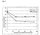
- Example 2 and Comparative Example 2 were subjected to ultraviolet irradiation at an intensity of 1 mW using a black light to determine the contact angle change.
- the results are shown in FIG. 2. It shows that the photo-inducted hydrophilicity was promoted by the oxygen plasma irradiation as in Example 1 and Comparative Example 1.
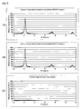
- FIG. 3 shows the X-ray diffraction pattern of an alkoxide film deposited in the same manner, but treated by oxygen plasma having an oxygen flow rate of 200 cc/minute (container pressure approx. 100 Pa). A peak indicating crystallization by the oxygen plasma treatment can be observed, from which it can be determined that this treatment formed a crystallized TiO 2 film from an alkoxide at room temperature.
- titanium alkoxide manufactured by Nippon Soda Co., Ltd. (NDH-510C) was deposited (a wet TiO 2 film) on a silicon wafer ((100) plane) by conducting a spin coating method for 20 seconds at 5000 rpm and dried in air at 120°C.
- the dried film was treated by ultraviolet rays having a wavelength of 253.7 nm for 1 hour with bubbled oxygen being flown into water of 60°C at a flow rate of 300 cc/minute.
- oxygen plasma having a frequency of 13.56 MHz, amplification power of 400 W and an internal pressure of 100 Pa for 10 minutes.
- titanium alkoxide manufactured by Nippon Soda Co., Ltd. (NDH-510C) was deposited (a wet TiO 2 film) on a silicon wafer ((100) plane) by conducting a spin coating method for 20 seconds at 5000 rpm and dried in air at 120°C.
- the dried film was treated by ultraviolet rays having a wavelength of 253.7 nm for 1 hour with bubbled oxygen being flown into water of 60°C at a flow rate of 300 cc/minute.
- oxygen plasma having a frequency of 13.56 MHz, amplification power of 500 W and an internal pressure of 100 Pa for 10 minutes.
- a film was prepared in the same manner as those in Examples 3 and 4, but without performing oxygen plasma treatment.
- the results are shown in FISG. 4(A) to 4(C).
- the X-ray diffraction patterns are shown in FIGS. 5(A) to 5(C). It shows that the contact angle was decreased by the ultraviolet irradiation, and the photo-inducted hydrophilicity was promoted by the oxygen plasma irradiation.
- a peak indicating crystallization by the plasma treatment can be observed, from which it can be determined that this treatment formed a crystallized TiO 2 film from an alkoxide at room temperature.
- FIG. 6 shows a view observed by a scanning electron microscope of the TiO 2 film obtained in Example 4. From this view, it can be seen that particles having a size of approximately 10 nm are packed very uniformly and densely.
- a film prepared in the same manner as those in Examples 3 and 4 was irradiated with oxygen plasma under the same conditions as Examples 3 and 4, but without the step of treating for 1 hour by ultraviolet rays having a wavelength of 253.7 nm for 1 hour with bubbled oxygen being flown into water of 60°C at a flow rate of 300 cc/minute.
- the results showed that the film was not crystallized nor cured, and cracks occurred in the entire surface.
- This example was conducted to confirm the dependency on an underlayer and the effects of a layered structure when a crystalline TiO 2 thin film is prepared from a wet TiO 2 film.
- titanium alkoxide manufactured by Nippon Soda Co., Ltd. Nippon Soda Co., Ltd. (NDH-510C) was deposited on silicon wafers ((100) plane; (110) plane; (111) plane) by conducting a spin coating method for 20 seconds at 5000 rpm (wet TiO 2 ) and dried in air at 120°C.
- the dried films were treated by ultraviolet rays having a wavelength of 253.7 nm for 1 hour with bubbled oxygen being flown into water of 60°C at a flow rate of 300 cc/minute.
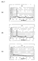
- Example 5 The X-ray diffraction patterns of Example 5 are shown in FIGS. 7(A) to 7(C).
- the degree of crystallization depends on Miller indices of the silicon wafer.
- the 3-layered film had a total film thickness of about 200 nm, and no cracks or peeling from the boundaries of the layered structure were observed. Consequently, it is possible to produce a thick film by providing a layered structure.
- titanium alkoxide manufactured by Nippon Soda Co., Ltd. (NDH-510C) was deposited on a silicon wafer ((100) plane) by conducting a spin coating method or 20 seconds at 3000 rpm (wet TiO 2 ) and dried in air at 120°C.
- the dried film was treated by ultraviolet rays having a wavelength of 253.7 nm for 1 hour with bubbled oxygen being flown into water of 60°C at a flow rate of 300 cc/minute.
- oxygen plasma having a frequency of 13.56 MHz, amplification power of 550 W and an internal pressure of 100 Pa for 3 minutes, 5 minutes and 10 minutes, respectively.
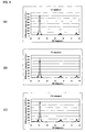
- the X-ray diffraction patterns of Example 6 are shown in FIGS. 8(A) to 8(C).
- Cross-sectional views of the films observed with a scanning electron microscope are shown in FIGS. 9(A) to 9(C). It can be seen from the changes in the X-ray diffraction patterns and the film thickness that a large part of the crystallization had been finished after only 3 minutes elapsed. According to measurement with a thermo-label, the surface temperature was still about 80°C when plasma irradiation was performed for 3 minutes, and the surface temperature was still about 180°C when plasma irradiation was performed for 10 minutes. This shows that the crystallization was not caused by heat such as self-heating or external heating.
- the refractive index of the film which was treated for 10 minutes in Example 6 was evaluated by ellipsometry, and the refractive index was 1.88 before the plasma treatment was conducted, and 2.33 after the plasma treatment was conducted.
- the refractive index of a similar film to that of Example 6 which was burned for 1 hour at 500°C in air without conducting plasma treatment was 2.24.
- the X-ray diffraction patterns of these film are shown in FIGS. 10(A) and 10(B). While the film (A) which was crystallized by heat had a large number of cracks, the film (B) which was obtained by plasma treatment was dense and homogenous. Also, from the fact that the refractive index of anatase is 2.46, it was assumed that the film underwent the plasma treatment for 10 minutes in Example 6 had a relative density of 90% or more.
- This example was conducted to confirm the electrical properties and the homogeneity of a crystalline TiO 2 thin film produced from a wet TiO 2 film.
- platinum was deposited onto a silicon wafer ((100) plane).
- titanium alkoxide manufactured by Nippon Soda Co., Ltd. NDH-510C was deposited by conducting a spin coating method for 20 seconds at 3000 rpm and dried in air at 120°C. The dried film was treated by ultraviolet rays having a wavelength of 253.7 nm for 1 hour with bubbled oxygen being flown into water of 60°C at a flow rate of 300 cc/minute.
- ITO a metal oxide thin film produced from sputtering ITO.
- ITO was deposited in an amount of about 150 nm on Pyrex and a silicon wafer ((100) plane) at room temperature, and thereafter irradiated with oxygen plasma or nitrogen plasma having a frequency of 13.56 MHz, amplification power of 550 W and an internal pressure of 100 Pa for 10 minutes.
- the X-ray diffraction patterns of Example 8 are shown in FIGS. 11(A) to 11(D). Although the degree of crystallization varies, crystallization occurred by both oxygen plasma and nitrogen plasma, and the degree of the crystallization depends on the type of plasma and the substrate.
- An ITO amorphous thin film was deposited by sputtering onto a polyethylene terephthalate film having a thickness of 50 ⁇ m at room temperature in mixed gas of argon gas of 295 CCM and oxygen gas of 5 CCM having a total pressure of 0.6 Pa, under conditions of a frequency of 13.56 MHz and amplification power of 1.5 KW, and oxygen plasma treatment was carried out under conditions of a frequency of 13.56 MHz, oxygen gas of 400 CCM, amplification power of 400 W and an internal pressure of 33 Pa.
- the graph of the resistance change in Example 9 is shown in FIG. 12. The graph shows that the resistance decreased almost straightly.
- Substance Deposition method Substrate Plasma type Presence of crystallization ITO sputtering Glass oxygen ⁇ ITO sputtering Glass nitrogen ⁇ ITO sputtering Si ⁇ 100> oxygen ⁇ ITO sputtering Si ⁇ 100> nitrogen ⁇ PbO 2 sol-gel Si ⁇ 111> oxygen ⁇ PZT sol-gel Si ⁇ 111> oxygen ⁇ Soda-lime glass sputtering Si ⁇ 111> oxygen ⁇ Al 2 O 3 sol-gel Glass oxygen ⁇ Al 2 O 3 sol-gel Si ⁇ 100> oxygen ⁇ TiO 2 sputtering Glass oxygen ⁇ TiO 2 sol-gel Glass oxygen ⁇ TiO 2 sol-gel Si ⁇ 100> oxygen ⁇
- a crystalline metal oxide thin film can be effectively formed on various substrates without requiring heating.
- This process overcomes the drawbacks of the conventional process and pioneers a new path for ta process for producing a thin film.
- a method for producing a metal oxide thin film according to the present invention can effectively form a dense and homogenous crystalline metal oxide thin film on a substrate at a low temperature without requiring active heat treatment. Accordingly, a metal oxide thin film having desired characteristics can be formed without damage to the characteristics of the substrate even if the substrate has a relatively low heat resistance. Consequently, the present invention can be applied, in particular, to all cases where a metal oxide thin film needs to be formed on a substrate having a low heat resistance such as resin.
Landscapes
- Chemical & Material Sciences (AREA)
- Organic Chemistry (AREA)
- Chemical Kinetics & Catalysis (AREA)
- Engineering & Computer Science (AREA)
- Materials Engineering (AREA)
- Mechanical Engineering (AREA)
- Metallurgy (AREA)
- Health & Medical Sciences (AREA)
- Inorganic Chemistry (AREA)
- Toxicology (AREA)
- General Chemical & Material Sciences (AREA)
- Oxygen, Ozone, And Oxides In General (AREA)
- Formation Of Insulating Films (AREA)
- Physical Vapour Deposition (AREA)
- Inorganic Compounds Of Heavy Metals (AREA)
- Catalysts (AREA)
- Other Surface Treatments For Metallic Materials (AREA)
- Physical Or Chemical Processes And Apparatus (AREA)
Applications Claiming Priority (5)
| Application Number | Priority Date | Filing Date | Title |
|---|---|---|---|
| JP2001306174 | 2001-10-02 | ||
| JP2001306174 | 2001-10-02 | ||
| JP2002077919 | 2002-03-20 | ||
| JP2002077919 | 2002-03-20 | ||
| PCT/JP2002/010181 WO2003031673A1 (en) | 2001-10-02 | 2002-09-30 | Thin metal oxide film and process for producing the same |
Publications (3)
| Publication Number | Publication Date |
|---|---|
| EP1452619A1 true EP1452619A1 (de) | 2004-09-01 |
| EP1452619A4 EP1452619A4 (de) | 2007-04-04 |
| EP1452619B1 EP1452619B1 (de) | 2011-09-14 |
Family
ID=26623582
Family Applications (1)
| Application Number | Title | Priority Date | Filing Date |
|---|---|---|---|
| EP02768137A Expired - Lifetime EP1452619B1 (de) | 2001-10-02 | 2002-09-30 | Verfahren zur herstellung vom dünnen metalloxidfilm |
Country Status (8)
| Country | Link |
|---|---|
| US (1) | US7132373B2 (de) |
| EP (1) | EP1452619B1 (de) |
| JP (2) | JP4235551B2 (de) |
| KR (2) | KR20090091831A (de) |
| CN (1) | CN100347333C (de) |
| AT (1) | ATE524574T1 (de) |
| TW (1) | TWI225105B (de) |
| WO (1) | WO2003031673A1 (de) |
Cited By (5)
| Publication number | Priority date | Publication date | Assignee | Title |
|---|---|---|---|---|
| WO2005031030A3 (de) * | 2003-09-22 | 2005-08-11 | Fraunhofer Ges Forschung | Verfahren zur plasmabehandlung einer oberfläche |
| EP2107133A1 (de) * | 2008-04-04 | 2009-10-07 | Nederlandse Organisatie voor toegepast- natuurwetenschappelijk onderzoek TNO | Verfahren zur Behandlung einer Metalloxidschicht |
| WO2012138458A1 (en) * | 2011-04-04 | 2012-10-11 | Guardian Industries Corp. | Methods of making a textured coating for thin- film solar cells |
| US10256291B2 (en) | 2009-07-17 | 2019-04-09 | Semiconductor Energy Laboratory Co., Ltd. | Method of manufacturing semiconductor device |
| EP3972002A4 (de) * | 2019-05-13 | 2022-12-07 | Boe Technology Group Co., Ltd. | Lichtemittierende vorrichtung und herstellungsverfahren dafür |
Families Citing this family (46)
| Publication number | Priority date | Publication date | Assignee | Title |
|---|---|---|---|---|
| KR100808790B1 (ko) * | 2003-05-23 | 2008-03-03 | 주식회사 엘지화학 | 질소 플라즈마 처리된 ito 필름 및 이를 양극으로사용한 유기 발광 소자 |
| WO2005077525A1 (ja) * | 2004-02-12 | 2005-08-25 | The University Of Tokyo | 結晶薄膜及びその製造方法 |
| JP2006096577A (ja) * | 2004-09-28 | 2006-04-13 | Tokyo Institute Of Technology | 金属酸化物膜、金属酸化物膜の製造方法および成形品 |
| DE112005002796T5 (de) * | 2004-11-10 | 2007-10-11 | Dai Nippon Printing Co., Ltd. | Verfahren zur Herstellung eines Metalloxidfilms |
| US7829444B2 (en) * | 2004-11-10 | 2010-11-09 | Canon Kabushiki Kaisha | Field effect transistor manufacturing method |
| JP2006179599A (ja) * | 2004-12-21 | 2006-07-06 | Toshiba Corp | 半導体装置およびその製造方法 |
| CN101527263B (zh) | 2005-02-17 | 2013-03-20 | 株式会社日立国际电气 | 半导体器件的制造方法 |
| JP4967272B2 (ja) * | 2005-08-02 | 2012-07-04 | 株式会社ブリヂストン | Cu2O薄膜の結晶化方法及びCu2O薄膜を有する積層体 |
| JP2007039270A (ja) * | 2005-08-02 | 2007-02-15 | Bridgestone Corp | 金属ドープTiO2薄膜の結晶化方法及び金属ドープTiO2薄膜を有する積層体 |
| US20070259127A1 (en) * | 2006-05-02 | 2007-11-08 | Sharp Laboratories Of America, Inc. | Method for densifying sol-gel films to form microlens structures |
| JP4789700B2 (ja) * | 2006-05-25 | 2011-10-12 | 株式会社シンクロン | 親水性薄膜の製造方法 |
| JP2008081344A (ja) * | 2006-09-27 | 2008-04-10 | Sekisui Chem Co Ltd | 酸化亜鉛の結晶化方法及び結晶膜形成装置 |
| JP2008255373A (ja) * | 2007-03-30 | 2008-10-23 | Univ Of Tokyo | 結晶薄膜及びその製造方法 |
| EP2011898B1 (de) * | 2007-07-03 | 2021-04-07 | Beneq Oy | Beschichtungsverfahren von metallischen Oxiden |
| JP5256694B2 (ja) * | 2007-10-31 | 2013-08-07 | 信越化学工業株式会社 | 酸化チタン系光触媒薄膜の製造法 |
| TWI365562B (en) * | 2008-10-03 | 2012-06-01 | Ind Tech Res Inst | Positive electrode and method for manufacturing the same and lithium battery utilizing the same |
| US8709681B2 (en) * | 2009-04-16 | 2014-04-29 | Hoya Corporation | Mask blank, transfer mask, and film denseness evaluation method |
| US8426763B2 (en) * | 2009-04-23 | 2013-04-23 | Micron Technology, Inc. | Rapid thermal processing systems and methods for treating microelectronic substrates |
| JPWO2011027872A1 (ja) * | 2009-09-04 | 2013-02-04 | 国立大学法人 東京大学 | 無機構造物及びその製造方法、並びに無機薄膜の製造方法 |
| JP5403293B2 (ja) * | 2009-11-05 | 2014-01-29 | 住友金属鉱山株式会社 | 透明導電膜の製造方法及び透明導電膜、それを用いた素子、透明導電基板並びにそれを用いたデバイス |
| US8528224B2 (en) * | 2009-11-12 | 2013-09-10 | Novellus Systems, Inc. | Systems and methods for at least partially converting films to silicon oxide and/or improving film quality using ultraviolet curing in steam and densification of films using UV curing in ammonia |
| JP5257372B2 (ja) * | 2009-11-30 | 2013-08-07 | 住友金属鉱山株式会社 | 酸化物蒸着材と透明導電膜および太陽電池 |
| US20120028011A1 (en) * | 2010-07-27 | 2012-02-02 | Chong Pyung An | Self-passivating mechanically stable hermetic thin film |
| GB201110117D0 (en) | 2011-06-16 | 2011-07-27 | Fujifilm Mfg Europe Bv | method and device for manufacturing a barrie layer on a flexible substrate |
| US8288297B1 (en) * | 2011-09-01 | 2012-10-16 | Intermolecular, Inc. | Atomic layer deposition of metal oxide materials for memory applications |
| EP2754170A4 (de) * | 2011-09-09 | 2015-04-29 | Panorama Synergy Ltd | Verfahren zum kristallisieren von dünnschichten |
| JP6028961B2 (ja) * | 2012-03-22 | 2016-11-24 | 国立研究開発法人産業技術総合研究所 | トランジスタ用酸化物半導体膜の製造方法 |
| JP6043506B2 (ja) * | 2012-05-16 | 2016-12-14 | 株式会社アルバック | 硬質化装置及び金属酸化物膜の硬質化方法 |
| CN105408244B (zh) * | 2013-08-07 | 2019-04-12 | 株式会社尼康 | 金属氧化物膜的制造方法和晶体管的制造方法 |
| US20160138182A1 (en) * | 2014-11-18 | 2016-05-19 | Wisconsin Alumni Research Foundation | Methods for forming mixed metal oxide epitaxial films |
| JP6449026B2 (ja) * | 2015-01-23 | 2019-01-09 | 国立研究開発法人産業技術総合研究所 | 半導体製造装置および半導体製造方法 |
| KR20160092699A (ko) * | 2015-01-28 | 2016-08-05 | 에스케이하이닉스 주식회사 | 저항변화 메모리 장치의 제조 방법 |
| CN104843771A (zh) * | 2015-04-24 | 2015-08-19 | 柳州百韧特先进材料有限公司 | 从废ito靶材中回收制备纳米ito粉体的方法 |
| CN107541724A (zh) * | 2016-06-27 | 2018-01-05 | 中国科学院金属研究所 | 一种形貌和成分可控的金属氧化物薄膜的制备方法 |
| JP6920656B2 (ja) * | 2017-06-07 | 2021-08-18 | パナソニックIpマネジメント株式会社 | 半導体電極及びそれを備えたデバイス、並びに、半導体電極の製造方法 |
| CN108039407B (zh) * | 2017-12-27 | 2021-10-26 | 佛山市卓膜科技有限公司 | 一种高取向的氧化物压电薄膜的制备方法及压电薄膜 |
| CN108110134B (zh) * | 2017-12-27 | 2021-04-23 | 佛山市卓膜科技有限公司 | 一种多取向氧化物压电薄膜的制备方法及压电薄膜 |
| US12534382B2 (en) | 2018-04-20 | 2026-01-27 | École De Technologie Supérieure | Amorphous titanium dioxide precursor material, method of producing thereof and method of controlling crystalline phases thereof |
| KR102710730B1 (ko) * | 2018-11-26 | 2024-09-27 | 삼성전자주식회사 | 유전체, 이를 포함하는 캐패시터 및 반도체 소자, 및 이의 제조방법 |
| CN111863600A (zh) * | 2019-04-30 | 2020-10-30 | 联芯集成电路制造(厦门)有限公司 | 增加固体材料层和流体材料层之间贴附性的方法 |
| CN113950764B (zh) * | 2019-05-29 | 2025-03-11 | 国立研究开发法人产业技术综合研究所 | 具有浸渗性的高密度脆性材料构造体 |
| CN114072680B (zh) * | 2019-07-10 | 2025-05-06 | 株式会社日立高新技术 | 自动分析装置以及自动分析装置的运转方法 |
| KR102715039B1 (ko) | 2019-10-21 | 2024-10-10 | 삼성전자주식회사 | 유전체, 이를 포함하는 커패시터, 반도체 소자, 및 이의 제조방법 |
| CN113410055B (zh) * | 2021-05-21 | 2022-10-25 | 嘉兴学院 | 一种低漏导高耐压固态电介质薄膜电容器及其制备方法 |
| CN119998052A (zh) * | 2022-10-11 | 2025-05-13 | 肖特股份有限公司 | 无定形涂层的等离子体诱导结晶和致密化 |
| CN119100608A (zh) * | 2024-10-12 | 2024-12-10 | 景德镇陶瓷大学 | 一种耐水耐酸碱的Na-Ca玻璃,其制备方法以及在制备浴室镜中的应用 |
Family Cites Families (40)
| Publication number | Priority date | Publication date | Assignee | Title |
|---|---|---|---|---|
| JPS62116773A (ja) * | 1985-11-15 | 1987-05-28 | Ricoh Co Ltd | 透明導電膜 |
| JPH089767B2 (ja) * | 1987-03-31 | 1996-01-31 | エヌオーケー株式会社 | 低抵抗透明導電膜の製造方法 |
| JP2593883B2 (ja) * | 1987-09-07 | 1997-03-26 | 岩尾磁器工業株式会社 | アルミナ−ジルコニア複合粉体とその焼結体の製造方法 |
| JPH02283022A (ja) | 1989-01-25 | 1990-11-20 | Hitachi Ltd | 半導体装置の製造方法 |
| JPH0429783A (ja) * | 1990-05-24 | 1992-01-31 | Sekisui Chem Co Ltd | 防曇プラスチックの製造方法 |
| JPH04149090A (ja) | 1990-10-09 | 1992-05-22 | Onoda Cement Co Ltd | 結晶質誘電体薄膜の作成方法 |
| JPH04199828A (ja) | 1990-11-29 | 1992-07-21 | Matsushita Electric Ind Co Ltd | 酸化物高誘電率薄膜の製造方法 |
| JPH04308616A (ja) * | 1991-04-08 | 1992-10-30 | Ricoh Co Ltd | 透明導電膜の製法 |
| US5631664A (en) * | 1992-09-18 | 1997-05-20 | Olympus Optical Co., Ltd. | Display system utilizing electron emission by polarization reversal of ferroelectric material |
| JP3293912B2 (ja) * | 1992-12-10 | 2002-06-17 | 松下電器産業株式会社 | 酸化物薄膜の形成方法 |
| JP2551721B2 (ja) * | 1993-02-10 | 1996-11-06 | 株式会社利根 | 多軸掘削方法及びその装置 |
| JP3397214B2 (ja) * | 1993-09-17 | 2003-04-14 | 松下電器産業株式会社 | 薄膜の形成方法 |
| JP3288515B2 (ja) * | 1994-02-15 | 2002-06-04 | 松下電器産業株式会社 | 透明導電性基板の製造方法 |
| JPH07294861A (ja) | 1994-04-21 | 1995-11-10 | Sumitomo Electric Ind Ltd | 酸化物誘電体薄膜およびその製造方法 |
| US5593737A (en) * | 1995-05-23 | 1997-01-14 | United Technologies Corporation | Photocatalytic semiconductor coating process |
| JPH0964307A (ja) | 1995-08-29 | 1997-03-07 | Hitachi Ltd | 酸化物薄膜の熱処理方法 |
| KR0165484B1 (ko) | 1995-11-28 | 1999-02-01 | 김광호 | 탄탈륨산화막 증착 형성방법 및 그 장치 |
| KR100207467B1 (ko) | 1996-02-29 | 1999-07-15 | 윤종용 | 반도체 장치의 커패시터 제조 방법 |
| JP3704792B2 (ja) | 1996-03-29 | 2005-10-12 | 松下電工株式会社 | 光触媒材料の製造方法 |
| KR100269314B1 (ko) | 1997-02-17 | 2000-10-16 | 윤종용 | 플라즈마처리를이용한반도체장치의커패시터제조방법 |
| JP3753204B2 (ja) | 1997-03-27 | 2006-03-08 | 日本電信電話株式会社 | 酸化物超伝導体薄膜の作製方法 |
| JPH10291885A (ja) * | 1997-04-15 | 1998-11-04 | Seiko Epson Corp | 酸化物セラミックス薄膜の製造方法 |
| JPH11145148A (ja) | 1997-11-06 | 1999-05-28 | Tdk Corp | 熱プラズマアニール装置およびアニール方法 |
| JP2000086242A (ja) | 1998-09-11 | 2000-03-28 | Seiko Epson Corp | 薄膜及びその作製方法 |
| US6278153B1 (en) * | 1998-10-19 | 2001-08-21 | Nec Corporation | Thin film capacitor formed in via |
| TW473459B (en) * | 1998-12-10 | 2002-01-21 | Ibm | Method for forming transparent conductive film using chemically amplified resist |
| JP3296312B2 (ja) | 1999-01-06 | 2002-06-24 | 日本電気株式会社 | 固体撮像装置およびその製造方法 |
| JP2001031681A (ja) | 1999-07-16 | 2001-02-06 | Noritake Co Ltd | 金属有機化合物および金属酸化物膜形成方法 |
| JP2001085639A (ja) | 1999-08-31 | 2001-03-30 | Vanguard Internatl Semiconductor Corp | 誘電体層の形成方法 |
| KR100363081B1 (ko) | 1999-09-16 | 2002-11-30 | 삼성전자 주식회사 | 박막 형성장치 |
| DE10049257B4 (de) | 1999-10-06 | 2015-05-13 | Samsung Electronics Co., Ltd. | Verfahren zur Dünnfilmerzeugung mittels atomarer Schichtdeposition |
| JP2001133466A (ja) | 1999-11-05 | 2001-05-18 | Toshiba Corp | 自動分析装置 |
| JP2001139313A (ja) * | 1999-11-11 | 2001-05-22 | Nec Corp | 酸化物膜の製造方法と強誘電体メモリの製造方法 |
| EP1777321A1 (de) * | 1999-11-25 | 2007-04-25 | Idemitsu Kosan Co., Ltd. | Sputtertarget, transparentes und leitendes Oxid sowie Verfahren zur Herstellung des Sputtertargets |
| KR100494322B1 (ko) * | 1999-12-22 | 2005-06-10 | 주식회사 하이닉스반도체 | 반도체 소자의 캐패시터 제조 방법 |
| KR100341407B1 (ko) * | 2000-05-01 | 2002-06-22 | 윤덕용 | 플라즈마 처리에 의한 리튬전이금속 산화물 박막의 결정화방법 |
| US6378153B1 (en) * | 2000-08-31 | 2002-04-30 | Richey Morgan | Multifunctional shovel attachment for an ice axe |
| US6441554B1 (en) * | 2000-11-28 | 2002-08-27 | Se Plasma Inc. | Apparatus for generating low temperature plasma at atmospheric pressure |
| US6432725B1 (en) * | 2001-09-28 | 2002-08-13 | Infineon Technologies Ag | Methods for crystallizing metallic oxide dielectric films at low temperature |
| TWI254080B (en) * | 2002-03-27 | 2006-05-01 | Sumitomo Metal Mining Co | Transparent conductive thin film, process for producing the same, sintered target for producing the same, and transparent, electroconductive substrate for display panel, and organic electroluminescence device |
-
2002
- 2002-09-30 US US10/491,527 patent/US7132373B2/en not_active Expired - Fee Related
- 2002-09-30 KR KR1020097017042A patent/KR20090091831A/ko not_active Ceased
- 2002-09-30 CN CNB028196279A patent/CN100347333C/zh not_active Expired - Fee Related
- 2002-09-30 KR KR1020047004818A patent/KR100922661B1/ko not_active Expired - Fee Related
- 2002-09-30 JP JP2003534641A patent/JP4235551B2/ja not_active Expired - Fee Related
- 2002-09-30 EP EP02768137A patent/EP1452619B1/de not_active Expired - Lifetime
- 2002-09-30 WO PCT/JP2002/010181 patent/WO2003031673A1/ja not_active Ceased
- 2002-09-30 AT AT02768137T patent/ATE524574T1/de not_active IP Right Cessation
- 2002-10-02 TW TW091122730A patent/TWI225105B/zh not_active IP Right Cessation
-
2008
- 2008-11-05 JP JP2008283962A patent/JP2009074178A/ja active Pending
Cited By (7)
| Publication number | Priority date | Publication date | Assignee | Title |
|---|---|---|---|---|
| WO2005031030A3 (de) * | 2003-09-22 | 2005-08-11 | Fraunhofer Ges Forschung | Verfahren zur plasmabehandlung einer oberfläche |
| EP2107133A1 (de) * | 2008-04-04 | 2009-10-07 | Nederlandse Organisatie voor toegepast- natuurwetenschappelijk onderzoek TNO | Verfahren zur Behandlung einer Metalloxidschicht |
| WO2009123459A1 (en) * | 2008-04-04 | 2009-10-08 | Nederlandse Organisatie Voor Toegepast-Natuurwetenschappelijk Onderzoek Tno | Method for treating a metal oxide layer |
| US8349642B2 (en) | 2008-04-04 | 2013-01-08 | Nederlandse Organisatie Voor Toegepast-Natuurwetenschappelijk Onderzoek Tno | Method for treating a metal oxide layer |
| US10256291B2 (en) | 2009-07-17 | 2019-04-09 | Semiconductor Energy Laboratory Co., Ltd. | Method of manufacturing semiconductor device |
| WO2012138458A1 (en) * | 2011-04-04 | 2012-10-11 | Guardian Industries Corp. | Methods of making a textured coating for thin- film solar cells |
| EP3972002A4 (de) * | 2019-05-13 | 2022-12-07 | Boe Technology Group Co., Ltd. | Lichtemittierende vorrichtung und herstellungsverfahren dafür |
Also Published As
| Publication number | Publication date |
|---|---|
| KR20090091831A (ko) | 2009-08-28 |
| US7132373B2 (en) | 2006-11-07 |
| KR100922661B1 (ko) | 2009-10-19 |
| EP1452619B1 (de) | 2011-09-14 |
| TWI225105B (en) | 2004-12-11 |
| ATE524574T1 (de) | 2011-09-15 |
| JPWO2003031673A1 (ja) | 2005-01-27 |
| CN1564876A (zh) | 2005-01-12 |
| WO2003031673A1 (en) | 2003-04-17 |
| KR20040071679A (ko) | 2004-08-12 |
| JP2009074178A (ja) | 2009-04-09 |
| EP1452619A4 (de) | 2007-04-04 |
| JP4235551B2 (ja) | 2009-03-11 |
| CN100347333C (zh) | 2007-11-07 |
| US20040241976A1 (en) | 2004-12-02 |
Similar Documents
| Publication | Publication Date | Title |
|---|---|---|
| US7132373B2 (en) | Thin metal oxide film and process for producing the same | |
| EP1633902B1 (de) | Physikalische dampfabscheidung titanhaltiger schichten | |
| Hishimone et al. | Methods of fabricating thin films for energy materials and devices | |
| TWI621726B (zh) | Transparent conductive film and method of producing the same | |
| TWI595512B (zh) | Transparent conductive film and its manufacturing method | |
| CN1179231A (zh) | 一种制备具有低漏电流和低极化疲劳性能的电器件的方法 | |
| KR101982906B1 (ko) | 투명 도전성 필름의 제조 방법 | |
| TWI676607B (zh) | 樹脂基板積層體及電子元件之製造方法 | |
| JP3766453B2 (ja) | 透明導電膜およびその製造方法 | |
| TW200811891A (en) | Thin film dielectrics with co-fired electrodes for capacitors and methods of making thereof | |
| JP3427362B2 (ja) | 誘電体薄膜堆積方法 | |
| KR100613405B1 (ko) | 전기장 결합형 플라즈마 화학 증착법에 의한 투명한 도전성 금속 복합박막의 제조방법 | |
| JP2001046884A (ja) | 光触媒酸化チタン膜の製造方法 | |
| JPH10226535A (ja) | 高電導性の透明導電膜の製造方法 | |
| Naoyama et al. | A Low Temperature Preparation of BaTiO3 Thin Film by Sol-Gel-Hydrothermal Treatment below 210° C | |
| JP2010192294A (ja) | 透明導電膜の製造方法、透明導電膜およびデバイス | |
| JPH08335561A (ja) | 薄膜構成体とその製造方法 | |
| JP2007231304A (ja) | 薄膜の製造方法及び製造装置、並びに成形体の製造方法 | |
| JP3985041B2 (ja) | 透明導電性膜の製造方法 | |
| JP2011256452A (ja) | 薄膜の製造方法 | |
| JPH09301798A (ja) | チタン酸ジルコン酸鉛薄膜の製造方法 | |
| JPS63307692A (ja) | 強誘電薄膜の形成方法 | |
| WO2005077525A1 (ja) | 結晶薄膜及びその製造方法 | |
| JP2007287836A (ja) | Sbt薄膜の形成方法 | |
| JPH01205426A (ja) | 酸化タンタル薄膜の製造方法 |
Legal Events
| Date | Code | Title | Description |
|---|---|---|---|
| PUAI | Public reference made under article 153(3) epc to a published international application that has entered the european phase |
Free format text: ORIGINAL CODE: 0009012 |
|
| 17P | Request for examination filed |
Effective date: 20040429 |
|
| AK | Designated contracting states |
Kind code of ref document: A1 Designated state(s): AT BE BG CH CY CZ DE DK EE ES FI FR GB GR IE IT LI LU MC NL PT SE SK TR |
|
| AX | Request for extension of the european patent |
Extension state: AL LT LV MK RO SI |
|
| RAP1 | Party data changed (applicant data changed or rights of an application transferred) |
Owner name: TOTO LTD. Owner name: TOUDAI TLO, LTD. |
|
| RIC1 | Information provided on ipc code assigned before grant |
Ipc: C23C 14/58 20060101ALI20070222BHEP Ipc: C23C 14/08 20060101ALI20070222BHEP Ipc: C23C 18/14 20060101ALI20070222BHEP Ipc: C23C 8/36 20060101AFI20030423BHEP Ipc: H01L 21/52 20060101ALI20070222BHEP Ipc: C01B 13/28 20060101ALI20070222BHEP Ipc: H01L 21/316 20060101ALI20070222BHEP |
|
| A4 | Supplementary search report drawn up and despatched |
Effective date: 20070305 |
|
| RAP1 | Party data changed (applicant data changed or rights of an application transferred) |
Owner name: TOTO LTD. Owner name: THE UNIVERSITY OF TOKYO |
|
| 17Q | First examination report despatched |
Effective date: 20070626 |
|
| RAP1 | Party data changed (applicant data changed or rights of an application transferred) |
Owner name: THE UNIVERSITY OF TOKYO |
|
| RAP1 | Party data changed (applicant data changed or rights of an application transferred) |
Owner name: NATIONAL INSTITUTE OF ADVANCED INDUSTRIAL SCIENCE |
|
| GRAP | Despatch of communication of intention to grant a patent |
Free format text: ORIGINAL CODE: EPIDOSNIGR1 |
|
| RTI1 | Title (correction) |
Free format text: PROCESS FOR PRODUCING A THIN METAL OXIDE FILM |
|
| GRAS | Grant fee paid |
Free format text: ORIGINAL CODE: EPIDOSNIGR3 |
|
| GRAA | (expected) grant |
Free format text: ORIGINAL CODE: 0009210 |
|
| AK | Designated contracting states |
Kind code of ref document: B1 Designated state(s): AT BE BG CH CY CZ DE DK EE ES FI FR GB GR IE IT LI LU MC NL PT SE SK TR |
|
| AX | Request for extension of the european patent |
Extension state: AL LT LV MK RO SI |
|
| REG | Reference to a national code |
Ref country code: GB Ref legal event code: FG4D |
|
| REG | Reference to a national code |
Ref country code: CH Ref legal event code: EP |
|
| REG | Reference to a national code |
Ref country code: IE Ref legal event code: FG4D |
|
| REG | Reference to a national code |
Ref country code: DE Ref legal event code: R096 Ref document number: 60241046 Country of ref document: DE Effective date: 20111201 |
|
| REG | Reference to a national code |
Ref country code: NL Ref legal event code: VDEP Effective date: 20110914 |
|
| PG25 | Lapsed in a contracting state [announced via postgrant information from national office to epo] |
Ref country code: FI Free format text: LAPSE BECAUSE OF FAILURE TO SUBMIT A TRANSLATION OF THE DESCRIPTION OR TO PAY THE FEE WITHIN THE PRESCRIBED TIME-LIMIT Effective date: 20110914 Ref country code: SE Free format text: LAPSE BECAUSE OF FAILURE TO SUBMIT A TRANSLATION OF THE DESCRIPTION OR TO PAY THE FEE WITHIN THE PRESCRIBED TIME-LIMIT Effective date: 20110914 |
|
| LTIE | Lt: invalidation of european patent or patent extension |
Effective date: 20110914 |
|
| PG25 | Lapsed in a contracting state [announced via postgrant information from national office to epo] |
Ref country code: AT Free format text: LAPSE BECAUSE OF FAILURE TO SUBMIT A TRANSLATION OF THE DESCRIPTION OR TO PAY THE FEE WITHIN THE PRESCRIBED TIME-LIMIT Effective date: 20110914 Ref country code: GR Free format text: LAPSE BECAUSE OF FAILURE TO SUBMIT A TRANSLATION OF THE DESCRIPTION OR TO PAY THE FEE WITHIN THE PRESCRIBED TIME-LIMIT Effective date: 20111215 Ref country code: CY Free format text: LAPSE BECAUSE OF FAILURE TO SUBMIT A TRANSLATION OF THE DESCRIPTION OR TO PAY THE FEE WITHIN THE PRESCRIBED TIME-LIMIT Effective date: 20110914 |
|
| REG | Reference to a national code |
Ref country code: AT Ref legal event code: MK05 Ref document number: 524574 Country of ref document: AT Kind code of ref document: T Effective date: 20110914 |
|
| PG25 | Lapsed in a contracting state [announced via postgrant information from national office to epo] |
Ref country code: BE Free format text: LAPSE BECAUSE OF FAILURE TO SUBMIT A TRANSLATION OF THE DESCRIPTION OR TO PAY THE FEE WITHIN THE PRESCRIBED TIME-LIMIT Effective date: 20110914 |
|
| PG25 | Lapsed in a contracting state [announced via postgrant information from national office to epo] |
Ref country code: CZ Free format text: LAPSE BECAUSE OF FAILURE TO SUBMIT A TRANSLATION OF THE DESCRIPTION OR TO PAY THE FEE WITHIN THE PRESCRIBED TIME-LIMIT Effective date: 20110914 Ref country code: MC Free format text: LAPSE BECAUSE OF NON-PAYMENT OF DUE FEES Effective date: 20110930 Ref country code: SK Free format text: LAPSE BECAUSE OF FAILURE TO SUBMIT A TRANSLATION OF THE DESCRIPTION OR TO PAY THE FEE WITHIN THE PRESCRIBED TIME-LIMIT Effective date: 20110914 |
|
| REG | Reference to a national code |
Ref country code: CH Ref legal event code: PL |
|
| PG25 | Lapsed in a contracting state [announced via postgrant information from national office to epo] |
Ref country code: NL Free format text: LAPSE BECAUSE OF FAILURE TO SUBMIT A TRANSLATION OF THE DESCRIPTION OR TO PAY THE FEE WITHIN THE PRESCRIBED TIME-LIMIT Effective date: 20110914 Ref country code: EE Free format text: LAPSE BECAUSE OF FAILURE TO SUBMIT A TRANSLATION OF THE DESCRIPTION OR TO PAY THE FEE WITHIN THE PRESCRIBED TIME-LIMIT Effective date: 20110914 Ref country code: IT Free format text: LAPSE BECAUSE OF FAILURE TO SUBMIT A TRANSLATION OF THE DESCRIPTION OR TO PAY THE FEE WITHIN THE PRESCRIBED TIME-LIMIT Effective date: 20110914 Ref country code: PT Free format text: LAPSE BECAUSE OF FAILURE TO SUBMIT A TRANSLATION OF THE DESCRIPTION OR TO PAY THE FEE WITHIN THE PRESCRIBED TIME-LIMIT Effective date: 20120116 |
|
| REG | Reference to a national code |
Ref country code: IE Ref legal event code: MM4A |
|
| PLBE | No opposition filed within time limit |
Free format text: ORIGINAL CODE: 0009261 |
|
| STAA | Information on the status of an ep patent application or granted ep patent |
Free format text: STATUS: NO OPPOSITION FILED WITHIN TIME LIMIT |
|
| PG25 | Lapsed in a contracting state [announced via postgrant information from national office to epo] |
Ref country code: IE Free format text: LAPSE BECAUSE OF NON-PAYMENT OF DUE FEES Effective date: 20110930 Ref country code: LI Free format text: LAPSE BECAUSE OF NON-PAYMENT OF DUE FEES Effective date: 20110930 Ref country code: CH Free format text: LAPSE BECAUSE OF NON-PAYMENT OF DUE FEES Effective date: 20110930 Ref country code: DK Free format text: LAPSE BECAUSE OF FAILURE TO SUBMIT A TRANSLATION OF THE DESCRIPTION OR TO PAY THE FEE WITHIN THE PRESCRIBED TIME-LIMIT Effective date: 20110914 |
|
| 26N | No opposition filed |
Effective date: 20120615 |
|
| REG | Reference to a national code |
Ref country code: DE Ref legal event code: R097 Ref document number: 60241046 Country of ref document: DE Effective date: 20120615 |
|
| PG25 | Lapsed in a contracting state [announced via postgrant information from national office to epo] |
Ref country code: ES Free format text: LAPSE BECAUSE OF FAILURE TO SUBMIT A TRANSLATION OF THE DESCRIPTION OR TO PAY THE FEE WITHIN THE PRESCRIBED TIME-LIMIT Effective date: 20111225 |
|
| PG25 | Lapsed in a contracting state [announced via postgrant information from national office to epo] |
Ref country code: LU Free format text: LAPSE BECAUSE OF NON-PAYMENT OF DUE FEES Effective date: 20110930 |
|
| PG25 | Lapsed in a contracting state [announced via postgrant information from national office to epo] |
Ref country code: BG Free format text: LAPSE BECAUSE OF FAILURE TO SUBMIT A TRANSLATION OF THE DESCRIPTION OR TO PAY THE FEE WITHIN THE PRESCRIBED TIME-LIMIT Effective date: 20111214 |
|
| PG25 | Lapsed in a contracting state [announced via postgrant information from national office to epo] |
Ref country code: TR Free format text: LAPSE BECAUSE OF FAILURE TO SUBMIT A TRANSLATION OF THE DESCRIPTION OR TO PAY THE FEE WITHIN THE PRESCRIBED TIME-LIMIT Effective date: 20110914 |
|
| PGFP | Annual fee paid to national office [announced via postgrant information from national office to epo] |
Ref country code: DE Payment date: 20140922 Year of fee payment: 13 |
|
| PGFP | Annual fee paid to national office [announced via postgrant information from national office to epo] |
Ref country code: GB Payment date: 20140919 Year of fee payment: 13 Ref country code: FR Payment date: 20140919 Year of fee payment: 13 |
|
| REG | Reference to a national code |
Ref country code: DE Ref legal event code: R119 Ref document number: 60241046 Country of ref document: DE |
|
| GBPC | Gb: european patent ceased through non-payment of renewal fee |
Effective date: 20150930 |
|
| REG | Reference to a national code |
Ref country code: FR Ref legal event code: ST Effective date: 20160531 |
|
| PG25 | Lapsed in a contracting state [announced via postgrant information from national office to epo] |
Ref country code: GB Free format text: LAPSE BECAUSE OF NON-PAYMENT OF DUE FEES Effective date: 20150930 Ref country code: DE Free format text: LAPSE BECAUSE OF NON-PAYMENT OF DUE FEES Effective date: 20160401 |
|
| PG25 | Lapsed in a contracting state [announced via postgrant information from national office to epo] |
Ref country code: FR Free format text: LAPSE BECAUSE OF NON-PAYMENT OF DUE FEES Effective date: 20150930 |