EP1453089A2 - Substrats à semi-conducteur de fiabilité améliorée - Google Patents
Substrats à semi-conducteur de fiabilité améliorée Download PDFInfo
- Publication number
- EP1453089A2 EP1453089A2 EP04012282A EP04012282A EP1453089A2 EP 1453089 A2 EP1453089 A2 EP 1453089A2 EP 04012282 A EP04012282 A EP 04012282A EP 04012282 A EP04012282 A EP 04012282A EP 1453089 A2 EP1453089 A2 EP 1453089A2
- Authority
- EP
- European Patent Office
- Prior art keywords
- circuit
- marginal
- etching
- brazing material
- metal plate
- Prior art date
- Legal status (The legal status is an assumption and is not a legal conclusion. Google has not performed a legal analysis and makes no representation as to the accuracy of the status listed.)
- Granted
Links
Images



Classifications
-
- H—ELECTRICITY
- H10—SEMICONDUCTOR DEVICES; ELECTRIC SOLID-STATE DEVICES NOT OTHERWISE PROVIDED FOR
- H10W—GENERIC PACKAGES, INTERCONNECTIONS, CONNECTORS OR OTHER CONSTRUCTIONAL DETAILS OF DEVICES COVERED BY CLASS H10
- H10W40/00—Arrangements for thermal protection or thermal control
- H10W40/20—Arrangements for cooling
- H10W40/25—Arrangements for cooling characterised by their materials
- H10W40/255—Arrangements for cooling characterised by their materials having a laminate or multilayered structure, e.g. direct bond copper [DBC] ceramic substrates
-
- C—CHEMISTRY; METALLURGY
- C04—CEMENTS; CONCRETE; ARTIFICIAL STONE; CERAMICS; REFRACTORIES
- C04B—LIME, MAGNESIA; SLAG; CEMENTS; COMPOSITIONS THEREOF, e.g. MORTARS, CONCRETE OR LIKE BUILDING MATERIALS; ARTIFICIAL STONE; CERAMICS; REFRACTORIES; TREATMENT OF NATURAL STONE
- C04B37/00—Joining burned ceramic articles with other burned ceramic articles or other articles by heating
- C04B37/02—Joining burned ceramic articles with other burned ceramic articles or other articles by heating with metallic articles
- C04B37/023—Joining burned ceramic articles with other burned ceramic articles or other articles by heating with metallic articles characterised by the interlayer used
- C04B37/026—Joining burned ceramic articles with other burned ceramic articles or other articles by heating with metallic articles characterised by the interlayer used consisting of metals or metal salts
-
- H—ELECTRICITY
- H05—ELECTRIC TECHNIQUES NOT OTHERWISE PROVIDED FOR
- H05K—PRINTED CIRCUITS; CASINGS OR CONSTRUCTIONAL DETAILS OF ELECTRIC APPARATUS; MANUFACTURE OF ASSEMBLAGES OF ELECTRICAL COMPONENTS
- H05K1/00—Printed circuits
- H05K1/02—Details
- H05K1/0271—Arrangements for reducing stress or warp in rigid printed circuit boards, e.g. caused by loads, vibrations or differences in thermal expansion
-
- H—ELECTRICITY
- H10—SEMICONDUCTOR DEVICES; ELECTRIC SOLID-STATE DEVICES NOT OTHERWISE PROVIDED FOR
- H10W—GENERIC PACKAGES, INTERCONNECTIONS, CONNECTORS OR OTHER CONSTRUCTIONAL DETAILS OF DEVICES COVERED BY CLASS H10
- H10W70/00—Package substrates; Interposers; Redistribution layers [RDL]
- H10W70/60—Insulating or insulated package substrates; Interposers; Redistribution layers
- H10W70/67—Insulating or insulated package substrates; Interposers; Redistribution layers characterised by their insulating layers or insulating parts
- H10W70/68—Shapes or dispositions thereof
-
- H—ELECTRICITY
- H10—SEMICONDUCTOR DEVICES; ELECTRIC SOLID-STATE DEVICES NOT OTHERWISE PROVIDED FOR
- H10W—GENERIC PACKAGES, INTERCONNECTIONS, CONNECTORS OR OTHER CONSTRUCTIONAL DETAILS OF DEVICES COVERED BY CLASS H10
- H10W70/00—Package substrates; Interposers; Redistribution layers [RDL]
- H10W70/60—Insulating or insulated package substrates; Interposers; Redistribution layers
- H10W70/67—Insulating or insulated package substrates; Interposers; Redistribution layers characterised by their insulating layers or insulating parts
- H10W70/69—Insulating materials thereof
- H10W70/692—Ceramics or glasses
-
- C—CHEMISTRY; METALLURGY
- C04—CEMENTS; CONCRETE; ARTIFICIAL STONE; CERAMICS; REFRACTORIES
- C04B—LIME, MAGNESIA; SLAG; CEMENTS; COMPOSITIONS THEREOF, e.g. MORTARS, CONCRETE OR LIKE BUILDING MATERIALS; ARTIFICIAL STONE; CERAMICS; REFRACTORIES; TREATMENT OF NATURAL STONE
- C04B2237/00—Aspects relating to ceramic laminates or to joining of ceramic articles with other articles by heating
- C04B2237/02—Aspects relating to interlayers, e.g. used to join ceramic articles with other articles by heating
- C04B2237/12—Metallic interlayers
- C04B2237/124—Metallic interlayers based on copper
-
- C—CHEMISTRY; METALLURGY
- C04—CEMENTS; CONCRETE; ARTIFICIAL STONE; CERAMICS; REFRACTORIES
- C04B—LIME, MAGNESIA; SLAG; CEMENTS; COMPOSITIONS THEREOF, e.g. MORTARS, CONCRETE OR LIKE BUILDING MATERIALS; ARTIFICIAL STONE; CERAMICS; REFRACTORIES; TREATMENT OF NATURAL STONE
- C04B2237/00—Aspects relating to ceramic laminates or to joining of ceramic articles with other articles by heating
- C04B2237/02—Aspects relating to interlayers, e.g. used to join ceramic articles with other articles by heating
- C04B2237/12—Metallic interlayers
- C04B2237/125—Metallic interlayers based on noble metals, e.g. silver
-
- C—CHEMISTRY; METALLURGY
- C04—CEMENTS; CONCRETE; ARTIFICIAL STONE; CERAMICS; REFRACTORIES
- C04B—LIME, MAGNESIA; SLAG; CEMENTS; COMPOSITIONS THEREOF, e.g. MORTARS, CONCRETE OR LIKE BUILDING MATERIALS; ARTIFICIAL STONE; CERAMICS; REFRACTORIES; TREATMENT OF NATURAL STONE
- C04B2237/00—Aspects relating to ceramic laminates or to joining of ceramic articles with other articles by heating
- C04B2237/02—Aspects relating to interlayers, e.g. used to join ceramic articles with other articles by heating
- C04B2237/12—Metallic interlayers
- C04B2237/126—Metallic interlayers wherein the active component for bonding is not the largest fraction of the interlayer
- C04B2237/127—The active component for bonding being a refractory metal
-
- C—CHEMISTRY; METALLURGY
- C04—CEMENTS; CONCRETE; ARTIFICIAL STONE; CERAMICS; REFRACTORIES
- C04B—LIME, MAGNESIA; SLAG; CEMENTS; COMPOSITIONS THEREOF, e.g. MORTARS, CONCRETE OR LIKE BUILDING MATERIALS; ARTIFICIAL STONE; CERAMICS; REFRACTORIES; TREATMENT OF NATURAL STONE
- C04B2237/00—Aspects relating to ceramic laminates or to joining of ceramic articles with other articles by heating
- C04B2237/30—Composition of layers of ceramic laminates or of ceramic or metallic articles to be joined by heating, e.g. Si substrates
- C04B2237/32—Ceramic
- C04B2237/34—Oxidic
- C04B2237/343—Alumina or aluminates
-
- C—CHEMISTRY; METALLURGY
- C04—CEMENTS; CONCRETE; ARTIFICIAL STONE; CERAMICS; REFRACTORIES
- C04B—LIME, MAGNESIA; SLAG; CEMENTS; COMPOSITIONS THEREOF, e.g. MORTARS, CONCRETE OR LIKE BUILDING MATERIALS; ARTIFICIAL STONE; CERAMICS; REFRACTORIES; TREATMENT OF NATURAL STONE
- C04B2237/00—Aspects relating to ceramic laminates or to joining of ceramic articles with other articles by heating
- C04B2237/30—Composition of layers of ceramic laminates or of ceramic or metallic articles to be joined by heating, e.g. Si substrates
- C04B2237/32—Ceramic
- C04B2237/36—Non-oxidic
- C04B2237/366—Aluminium nitride
-
- C—CHEMISTRY; METALLURGY
- C04—CEMENTS; CONCRETE; ARTIFICIAL STONE; CERAMICS; REFRACTORIES
- C04B—LIME, MAGNESIA; SLAG; CEMENTS; COMPOSITIONS THEREOF, e.g. MORTARS, CONCRETE OR LIKE BUILDING MATERIALS; ARTIFICIAL STONE; CERAMICS; REFRACTORIES; TREATMENT OF NATURAL STONE
- C04B2237/00—Aspects relating to ceramic laminates or to joining of ceramic articles with other articles by heating
- C04B2237/30—Composition of layers of ceramic laminates or of ceramic or metallic articles to be joined by heating, e.g. Si substrates
- C04B2237/40—Metallic
- C04B2237/407—Copper
-
- C—CHEMISTRY; METALLURGY
- C04—CEMENTS; CONCRETE; ARTIFICIAL STONE; CERAMICS; REFRACTORIES
- C04B—LIME, MAGNESIA; SLAG; CEMENTS; COMPOSITIONS THEREOF, e.g. MORTARS, CONCRETE OR LIKE BUILDING MATERIALS; ARTIFICIAL STONE; CERAMICS; REFRACTORIES; TREATMENT OF NATURAL STONE
- C04B2237/00—Aspects relating to ceramic laminates or to joining of ceramic articles with other articles by heating
- C04B2237/50—Processing aspects relating to ceramic laminates or to the joining of ceramic articles with other articles by heating
- C04B2237/70—Forming laminates or joined articles comprising layers of a specific, unusual thickness
-
- H—ELECTRICITY
- H05—ELECTRIC TECHNIQUES NOT OTHERWISE PROVIDED FOR
- H05K—PRINTED CIRCUITS; CASINGS OR CONSTRUCTIONAL DETAILS OF ELECTRIC APPARATUS; MANUFACTURE OF ASSEMBLAGES OF ELECTRICAL COMPONENTS
- H05K1/00—Printed circuits
- H05K1/02—Details
- H05K1/03—Use of materials for the substrate
- H05K1/0306—Inorganic insulating substrates, e.g. ceramic, glass
-
- H—ELECTRICITY
- H05—ELECTRIC TECHNIQUES NOT OTHERWISE PROVIDED FOR
- H05K—PRINTED CIRCUITS; CASINGS OR CONSTRUCTIONAL DETAILS OF ELECTRIC APPARATUS; MANUFACTURE OF ASSEMBLAGES OF ELECTRICAL COMPONENTS
- H05K2201/00—Indexing scheme relating to printed circuits covered by H05K1/00
- H05K2201/03—Conductive materials
- H05K2201/0332—Structure of the conductor
- H05K2201/0335—Layered conductors or foils
- H05K2201/0355—Metal foils
-
- H—ELECTRICITY
- H05—ELECTRIC TECHNIQUES NOT OTHERWISE PROVIDED FOR
- H05K—PRINTED CIRCUITS; CASINGS OR CONSTRUCTIONAL DETAILS OF ELECTRIC APPARATUS; MANUFACTURE OF ASSEMBLAGES OF ELECTRICAL COMPONENTS
- H05K2201/00—Indexing scheme relating to printed circuits covered by H05K1/00
- H05K2201/09—Shape and layout
- H05K2201/09145—Edge details
-
- H—ELECTRICITY
- H05—ELECTRIC TECHNIQUES NOT OTHERWISE PROVIDED FOR
- H05K—PRINTED CIRCUITS; CASINGS OR CONSTRUCTIONAL DETAILS OF ELECTRIC APPARATUS; MANUFACTURE OF ASSEMBLAGES OF ELECTRICAL COMPONENTS
- H05K2201/00—Indexing scheme relating to printed circuits covered by H05K1/00
- H05K2201/09—Shape and layout
- H05K2201/09209—Shape and layout details of conductors
- H05K2201/09654—Shape and layout details of conductors covering at least two types of conductors provided for in H05K2201/09218 - H05K2201/095
- H05K2201/098—Special shape of the cross-section of conductors, e.g. very thick plated conductors
-
- H—ELECTRICITY
- H05—ELECTRIC TECHNIQUES NOT OTHERWISE PROVIDED FOR
- H05K—PRINTED CIRCUITS; CASINGS OR CONSTRUCTIONAL DETAILS OF ELECTRIC APPARATUS; MANUFACTURE OF ASSEMBLAGES OF ELECTRICAL COMPONENTS
- H05K2201/00—Indexing scheme relating to printed circuits covered by H05K1/00
- H05K2201/09—Shape and layout
- H05K2201/09818—Shape or layout details not covered by a single group of H05K2201/09009 - H05K2201/09809
- H05K2201/09845—Stepped hole, via, edge, bump or conductor
-
- H—ELECTRICITY
- H05—ELECTRIC TECHNIQUES NOT OTHERWISE PROVIDED FOR
- H05K—PRINTED CIRCUITS; CASINGS OR CONSTRUCTIONAL DETAILS OF ELECTRIC APPARATUS; MANUFACTURE OF ASSEMBLAGES OF ELECTRICAL COMPONENTS
- H05K3/00—Apparatus or processes for manufacturing printed circuits
- H05K3/38—Improvement of the adhesion between the insulating substrate and the metal
Definitions
- This invention relates to circuit substrates made of high-strength ceramic-metal composites. More particularly, the invention relates to semiconductor substrates of high reliability that have sufficiently high heat cycle characteristics to be suitable for use as circuit boards in automobiles, electric trains and other applications that require high output power.
- Ceramic circuit substrates having current conducting circuits are extensively used for mounting electronic components that generate large amounts of heat such as power hybrid ICs and power modules.
- various design considerations have been adopted in the fabrication of ceramic substrates and the formation of current carrying circuits with a view to manufacturing AlN ceramic circuit boards having high heat conductivity.
- circuit boards manufactured by those methods are improved in heat cycle characteristics compared to the circuit boards having no steps at all in the marginal portions and can withstand up to several hundred cycles without cracking.
- circuit boards for handling large power or those to be used in automobiles are required to have even higher operational reliability and withstand at least 1,500 heat cycles and no satisfactory substrates have so far been developed by adopting the above-described methods.
- the present invention has been accomplished under these circumstances and has as an object providing a power module circuit board that can withstand at least 1,500 heat cycles and which, hence, is suitable for use in automobiles and electric trains.
- the present inventors conducted intensive studies in order to attain the stated object and found that the heat cycle characteristics of a circuit board could be markedly improved by providing at least three steps in its marginal portions and also specifying their thickness and width.
- the present invention has been accomplished on the basis of this finding.
- the present invention relates generally to a semiconductor substrate of high reliability which comprises a ceramic to metal joined circuit board having three or more steps formed in the marginal portions of at least the conductor circuit.
- the lowest step in the marginal portions of the conductor circuit is made of an active metallic brazing material whereas the other steps are made of a metal or metals.
- all steps in the marginal portions of the conductor circuit are made of a metal or metals.
- the lowest step is made of an active metallic brazing material, with the active metal being at least one of Ti, Zr and Hf, whereas the other steps are made of a metal or metals.
- the lowest step has a thickness t 1 which accounts for no more 15% of the total thickness of the conductor and has a width l 1 of 5 - 500 ⁇ m
- the middle step has a thickness t 2 which accounts for 25 - 55% of the total thickness of the conductor and has a width l 2 of 100 - 500 ⁇ m
- the highest step has a thickness t 3 which accounts for 30 - 60% of the total thickness of the conductor, with t 1 + t 2 being no more than 70% of the total thickness of the conductor and l 1 + l 2 being no more than 1 mm.
- the ceramic substrate to be used in the invention is either an alumina substrate or a nitride ceramic substrate comprising aluminum nitride or silicon nitride.
- the conductor circuit is formed of a metal (i.e., Cu) plate.
- three or more steps can be formed in the marginal portions of a conductor circuit by two different methods depending on how the copper plate is joined to a ceramic substrate.
- an active metal process in which the copper plate is joined to the ceramic substrate using an active metallic brazing material, the following method is employed: a paste of the active metallic brazing material is applied to the entire surface on either side of the ceramic substrate (e.g.
- a circuit forming copper plate 0.3 mm thick is placed in contact with one surface of the substrate and a heat dissipating copper plate 0.25 mm thick in contact with the other surface; the three members are compressed together and heated at 850°C in a vacuum furnace to form a joint; an etching resist is applied to the circuit forming copper plate on the joint and after etching with an iron chloride solution to form a circuit pattern, the unwanted brazing material is removed from the marginal portions to form a first marginal step; then, a second resist layer is applied and etching is performed on the circuit forming Cu plate with an iron chloride solution to form a second marginal step; subsequently, a third resist layer is applied and etching is performed with an iron chloride solution to form a third marginal step.
- the thus completed conductor circuit has the lowest marginal step formed solely or partly of brazing material.
- the first marginal step i.e., the lowest step
- the first marginal step can be formed of either a single layer of the brazing material or a dual layer consisting of the brazing material and copper in a desired thickness.
- a circuit forming copper plate 0.3 mm thick is placed in contact with one surface of the ceramic (typically alumina) substrate and a heat dissipating copper plate 0.25 mm thick placed in contact with the other surface; the three members are compressed together and heated at 1,063°C in a heating furnace to form a joint; then, as in the active metal process, an etching resist is applied to the circuit forming copper plate on the joint and etching is performed with an iron chloride solution to form a circuit pattern having a first marginal step; subsequently, a second resist layer is applied and etching is performed with an iron chloride solution to form a second marginal step; finally, a third resist layer is applied and etching is performed with an iron chloride solution to form a third marginal step.
- the thus completed circuit board has three steps formed in the marginal portions of the circuit forming Cu plate.
- circuit boards having three steps formed in the marginal portions by the two processes were evaluated for their heat cycle characteristics, with each cycle consisting of heating at 125°C for 30 minutes and cooling at -40°C for 30 minutes. They could withstand at least 1,500 cycles, the result being uncomparable to the data obtained with the prior art version.
- marginal steps may be provided not only on the circuit forming copper plate but also on the heat dissipating copper plate on the other side of the substrate and this is also included within the scope of the invention.
- the circuit boards whether they were fabricated by the active metal process or the direct bonding process, could withstand at least 2,000 heat cycles without cracking.
- an etching resist was applied to the circuit forming copper plate and etching was performed with an iron chloride solution to form a circuit pattern and the unwanted brazing material removed from the marginal portions.
- a third resist layer was applied and etched to form a third marginal step.
- two pairs of circuit boards were fabricated which had the marginal profiles shown in Figs. 1A and 1B with the lowest step being made solely or partly of the brazing material.
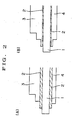
- Example 1 The other member of each of the circuit board pairs fabricated in Example 1 was further treated to form two steps in the marginal portions of the heat dissipating surface on the opposite side by resist application and etching (see Figs. 2A and 2B).
- the heat cycle characteristics of these circuit boards were tested by the same method as in Example 1. The results are also shown in Table 1; both circuit boards could withstand up to 2,000 cycles without cracking, thus proving to possess by far better heat cycle characteristics than the prior art version.
- a paste of brazing material 2 comprising 71.0% Ag, 16.5% Cu and 2.5% Ti was applied to the entire surface of either side of each substrate.
- a circuit forming copper plate 3 having a thickness of 0.3 mm was placed in contact with one surface of each substrate and a heat dissipating copper plate 4 having a thickness of 0.25 mm placed in contact with the other surface. The individual members were compressed together and heated at 850°C in a vacuum furnace to form a joint.
- an etching resist was applied to the circuit forming copper plate and etching was performed with an iron chloride solution to form a circuit pattern and the unwanted brazing material removed from the marginal portions.
- a third resist layer was applied and etched to form a third marginal step.
- two pairs of circuit boards were fabricated which had the marginal profiles shown in Figs. 1A and 1B with the lowest step being made solely or partly of the brazing material.
- Example 3 The other member of each of the circuit board pairs fabricated in Example 3 was further treated to form two steps in the marginal portions of the heat dissipating surface on the opposite side by resist application and etching (see Figs. 4A and 4B).
- the heat cycle characteristics of these circuit boards were tested by the same method as in Example 3. The results are also shown in Table 1; both circuit boards could withstand up to 2,000 cycles without cracking, thus proving to possess by far better heat cycle characteristics than the prior art versions.
- alumina substrates measuring 53 X 29 X 0.635 mm were provided as ceramic substrates 1.
- a circuit forming copper plate 3 having a thickness of 0.3 mm was placed in contact with one surface of each substrate and a heat dissipating copper plate 4 having a thickness of 0.25 mm placed in contact with the other surface.
- the individual members were compressed together and heated at 1,063°C in a heating furnace to have the copper plates bonded to the substrate directly.
- an etching resist was applied to the circuit forming copper plate and etching was performed with an iron chloride solution to form a circuit pattern having a first step in the marginal portions.
- a third resist layer was applied and etched to form a third marginal step. In this way, two pairs of circuit boards were fabricated which had the marginal profiles shown in Figs. 3A and 3B.
- Example 5 The other member of each of the circuit board pairs fabricated in Example 5 was further treated to form two steps in the marginal portions of the heat dissipating surface on the other side by resist application and etching (see Figs. 4A and 4B).
- the heat cycle characteristics of these circuit boards were tested by the same method as in Example 5. The results are also shown in Table 1; both circuit boards could withstand up to 2,000 cycles without cracking, thus proving to possess by far better heat cycle characteristics than the prior art versions.
- Two aluminum nitride substrates measuring 53 X 29 X 0.635 mm were provided as ceramic substrates 1.
- a paste of brazing material 2 comprising 71.0% Ag, 16.5% Cu, 2.0% Ti and 0.5% TiO 2 was applied to the entire surface of either side of each substrate.
- a circuit forming copper plate 3 having a thickness of 0.3 mm was placed in contact with one surface of each substrate and a heat dissipating copper plate 4 having a thickness of 0.25 mm placed in contact with the other surface.
- the individual members were compressed together and heated at 850°C in a vacuum furnace to form a joint.
- an etching resist was applied to the circuit forming copper plate and etching was performed with an iron chloride solution to form a circuit pattern and the unwanted brazing material removed from the marginal portions.
- a third marginal step was then formed by exclusively removing the Cu component with a chemical polishing solution, thereby fabricating two circuit boards which had the marginal profile shown in Fig. 1A with the lowest step being made solely of the brazing material.
- circuit board was subjected to a heat cycle test, each cycle consisting of heating at 125°C for 30 minutes and cooling at -40°C for 30 minutes. The results are shown in Table 1; the circuit board could withstand up to 1,500 cycles without cracking and fine cracks developed only after 2,000 cycles.
- Example 7 The other of the two circuit boards fabricated in Example 7 was further treated to form two marginal steps on the heat dissipating side by application of two resist layers and etching (see Fig. 2A).
- the heat cycle characteristics of the circuit board were tested by the same method as in Example 7 and the results are also shown in Table 1.
- the circuit board could withstand 2,000 cycles without cracking, thus proving to possess by far better heat cycle characteristics than the prior art version.
- Aluminum nitride and alumina substrates each measuring 53 X 29 X 0.635 mm were provided as ceramic substrates 1.
- a paste of the same active metallic brazing material 2 as used in Example 1 was applied to the entire surface of either side of the AlN substrate; a circuit forming copper plate 3 having a thickness of 0.3 mm and a heat dissipating copper plate 4 having a thickness of 0.25 mm were placed in contact with opposite sides of the substrate; the individual members were compressed together and heated at 850°C in a vacuum furnace to form a joint.
- the circuit forming copper plate 3 and the heat dissipating copper plate 4 of the thicknesses specified above were placed in opposite sides of the Al 2 O 3 substrate; and the individual members were compressed together and heated at 1,063°C in a heating furnace to form a joint.
- Two aluminum nitride substrates measuring 53 X 29 X 0.635 mm were provided as ceramic substrates 1.
- a paste of brazing material 2 comprising 71.0% Ag, 16.5% Cu and 2.5% Ti was applied to the entire surface of either side of each substrate.
- a circuit forming copper plate 3 having a thickness of 0.3 mm and a heat dissipating copper plate 4 having a thickness of 0.25 mm were placed in contact with opposite sides of each substrate, and the individual members were compressed together and heated at 850°C in a vacuum furnace to form a joint.
- an etching resist was applied to the circuit forming copper plate 3 and etching was performed with an iron chloride solution to form a circuit pattern and the unwanted brazing material was removed from the marginal portions.
- a second resist layer was applied over an area smaller than the Cu pattern and etching was performed with an iron chloride solution to fabricate two circuit boards having the marginal profiles shown in Figs. 6A and 6B.
- the two completed circuit boards one having a marginal step on the heat dissipation side (Fig. 6B) and the other having not (Fig. 6A), were subjected to a heat cycle test and the results are also shown in Table 1.
- the stepless circuit board could withstand up to 300 cycles without cracking; however, fine cracks developed after 400 cycles.
- the other circuit board could withstand up to 400 cycles; however, fine cracks developed after 500 cycles.
- Two alumina substrates measuring 53 X 29 X 0.635 mm were provided as ceramic substrates 1. Copper plates were placed in contact with opposite sides of each substrate, compressed together and heated at 1,063°C in a nitrogen gas atmosphere to form a joint. An etching resist was applied to the circuit forming copper plate and etching was performed with an iron chloride solution to form a circuit pattern.
- a second resist layer was applied over an area smaller than the Cu pattern and etching was performed with an iron chloride solution to fabricate two circuit boards having the marginal profiles shown in Fig. 7A and 7B.
- the two completed circuit boards one having marginal step on the heat dissipation side (Fig. 7B) and the other having not (Fig. 7A), were subjected to a heat cycle test and the results are also shown in Table 1.
- the stepless circuit board could withstand up to 300 cycles without cracking; however, fine cracks developed after 400 cycles.
- the other circuit board could withstand up to 400 cycles; however, fine cracks developed after 500 cycles.
- the circuit board of the invention which has three or more steps formed in the marginal portions of at least the conductor circuit is significantly improved in heat cycle characteristics compared to the conventional version having no more than two marginal steps. Due to this great improvement in heat cycle characteristics, the circuit board of the invention can be used with power modules in automobiles, electric trains and other heretofore impractical applications that require high output power.
Landscapes
- Engineering & Computer Science (AREA)
- Chemical & Material Sciences (AREA)
- Ceramic Engineering (AREA)
- Microelectronics & Electronic Packaging (AREA)
- Materials Engineering (AREA)
- Structural Engineering (AREA)
- Organic Chemistry (AREA)
- Manufacturing Of Printed Circuit Boards (AREA)
- Ceramic Products (AREA)
Applications Claiming Priority (5)
| Application Number | Priority Date | Filing Date | Title |
|---|---|---|---|
| JP24407696 | 1996-08-27 | ||
| JP24407696 | 1996-08-27 | ||
| JP08438997A JP3512977B2 (ja) | 1996-08-27 | 1997-03-18 | 高信頼性半導体用基板 |
| JP8438997 | 1997-03-18 | ||
| EP97810603A EP0827198B1 (fr) | 1996-08-27 | 1997-08-27 | Substrats métallo-céramiques de fiabilité améliorée pour semi-conducteurs |
Related Parent Applications (2)
| Application Number | Title | Priority Date | Filing Date |
|---|---|---|---|
| EP97810603A Division EP0827198B1 (fr) | 1996-08-27 | 1997-08-27 | Substrats métallo-céramiques de fiabilité améliorée pour semi-conducteurs |
| EP97810603.7 Division | 1997-08-27 |
Publications (3)
| Publication Number | Publication Date |
|---|---|
| EP1453089A2 true EP1453089A2 (fr) | 2004-09-01 |
| EP1453089A3 EP1453089A3 (fr) | 2004-09-08 |
| EP1453089B1 EP1453089B1 (fr) | 2013-02-20 |
Family
ID=26425436
Family Applications (2)
| Application Number | Title | Priority Date | Filing Date |
|---|---|---|---|
| EP97810603A Expired - Lifetime EP0827198B1 (fr) | 1996-08-27 | 1997-08-27 | Substrats métallo-céramiques de fiabilité améliorée pour semi-conducteurs |
| EP04012282A Expired - Lifetime EP1453089B1 (fr) | 1996-08-27 | 1997-08-27 | Substrats à semi-conducteur de fiabilité améliorée |
Family Applications Before (1)
| Application Number | Title | Priority Date | Filing Date |
|---|---|---|---|
| EP97810603A Expired - Lifetime EP0827198B1 (fr) | 1996-08-27 | 1997-08-27 | Substrats métallo-céramiques de fiabilité améliorée pour semi-conducteurs |
Country Status (4)
| Country | Link |
|---|---|
| US (1) | US6054762A (fr) |
| EP (2) | EP0827198B1 (fr) |
| JP (1) | JP3512977B2 (fr) |
| DE (1) | DE69730388T2 (fr) |
Cited By (1)
| Publication number | Priority date | Publication date | Assignee | Title |
|---|---|---|---|---|
| WO2012025294A1 (fr) * | 2010-08-25 | 2012-03-01 | Robert Bosch Gmbh | Procédé de réalisation d'un circuit électrique et circuit électrique |
Families Citing this family (45)
| Publication number | Priority date | Publication date | Assignee | Title |
|---|---|---|---|---|
| EP0935286A4 (fr) * | 1997-05-26 | 2008-04-09 | Sumitomo Electric Industries | Substrat jonction de circuit en cuivre et procede de production de ce substrat |
| US6222261B1 (en) * | 1999-05-03 | 2001-04-24 | The United States Of America As Represented By The Secretary Of The Army | Barrier layers for thin film electronic materials |
| DE19927046B4 (de) * | 1999-06-14 | 2007-01-25 | Electrovac Ag | Keramik-Metall-Substrat als Mehrfachsubstrat |
| EP1063700B1 (fr) * | 1999-06-22 | 2012-07-25 | Infineon Technologies AG | Substrat pour des modules haute tension |
| JP4158288B2 (ja) * | 1999-08-31 | 2008-10-01 | 三菱電機株式会社 | 半導体モジュール |
| JP2001156413A (ja) * | 1999-11-26 | 2001-06-08 | Sumitomo Electric Ind Ltd | 銅回路接合基板及びその製造方法 |
| US7019975B2 (en) * | 2000-08-09 | 2006-03-28 | Mitsubishi Materials Corporation | Power module and power module with heat sink |
| JP4756200B2 (ja) | 2000-09-04 | 2011-08-24 | Dowaメタルテック株式会社 | 金属セラミックス回路基板 |
| DE10158185B4 (de) * | 2000-12-20 | 2005-08-11 | Semikron Elektronik Gmbh | Leistungshalbleitermodul mit hoher Isolationsfestigkeit |
| US6936337B2 (en) | 2001-09-28 | 2005-08-30 | Dowa Mining Co., Ltd. | Metal/ceramic circuit board |
| JP4811756B2 (ja) * | 2001-09-28 | 2011-11-09 | Dowaメタルテック株式会社 | 金属−セラミックス接合回路基板の製造方法 |
| JP4168114B2 (ja) * | 2001-09-28 | 2008-10-22 | Dowaホールディングス株式会社 | 金属−セラミックス接合体 |
| JP3648189B2 (ja) * | 2001-09-28 | 2005-05-18 | 同和鉱業株式会社 | 金属−セラミックス回路基板 |
| JP2005520334A (ja) * | 2002-03-13 | 2005-07-07 | スチュルス−ハーダー,ジャーヘン | 金属−セラミック基板、好ましくは銅−セラミック基板を製造するプロセス |
| DE10212495B4 (de) | 2002-03-21 | 2004-02-26 | Schulz-Harder, Jürgen, Dr.-Ing. | Verfahren zum Herstellen eines Metall-Keramik-Substrats, vorzugsweise eines Kupfer-Keramik-Substrats |
| JP3863067B2 (ja) * | 2002-06-04 | 2006-12-27 | Dowaホールディングス株式会社 | 金属−セラミックス接合体の製造方法 |
| JP3868854B2 (ja) * | 2002-06-14 | 2007-01-17 | Dowaホールディングス株式会社 | 金属−セラミックス接合体およびその製造方法 |
| JP4401096B2 (ja) * | 2003-03-26 | 2010-01-20 | Dowaホールディングス株式会社 | 回路基板の製造方法 |
| JP4394477B2 (ja) * | 2003-03-27 | 2010-01-06 | Dowaホールディングス株式会社 | 金属−セラミックス接合基板の製造方法 |
| JP5299160B2 (ja) * | 2003-03-27 | 2013-09-25 | Dowaメタルテック株式会社 | 金属−セラミックス接合基板の製造方法 |
| JP4127131B2 (ja) * | 2003-06-25 | 2008-07-30 | 松下電工株式会社 | 調光装置 |
| US7532481B2 (en) * | 2004-04-05 | 2009-05-12 | Mitsubishi Materials Corporation | Al/AlN joint material, base plate for power module, power module, and manufacturing method of Al/AlN joint material |
| US8563869B2 (en) | 2005-08-29 | 2013-10-22 | Hitachi Metals, Ltd. | Circuit board and semiconductor module using this, production method for circuit board |
| DE102009033029A1 (de) | 2009-07-02 | 2011-01-05 | Electrovac Ag | Elektronische Vorrichtung |
| DE102011103746A1 (de) | 2011-05-31 | 2012-12-06 | Ixys Semiconductor Gmbh | Verfahren zum Fügen von Metall-Keramik-Substraten an Metallkörpern |
| CN104011852B (zh) * | 2011-12-20 | 2016-12-21 | 株式会社东芝 | 陶瓷铜电路基板和使用了陶瓷铜电路基板的半导体装置 |
| DE102013102637B4 (de) * | 2013-03-14 | 2017-08-31 | Rogers Germany Gmbh | Metall-Keramik-Substrat sowie Verfahren zum Herstellen eines derartigen Metall-Keramik-Substrates und Anordnung von derartigen Metall-Keramik-Substraten |
| DE102013104739B4 (de) * | 2013-03-14 | 2022-10-27 | Rogers Germany Gmbh | Metall-Keramik-Substrate sowie Verfahren zum Herstellen eines Metall-Keramik-Substrates |
| EP2916627B1 (fr) * | 2013-08-29 | 2019-04-03 | Hitachi Metals, Ltd. | Procédé de fabrication de carte de circuit céramique |
| DE112013007709T5 (de) * | 2013-12-24 | 2016-09-15 | Mitsubishi Electric Corporation | Elektrischer Leistungswandler und Leistungsmodul |
| EP3093882B1 (fr) * | 2014-01-10 | 2021-02-17 | Furukawa Electric Co. Ltd. | Dispositif de circuit électronique |
| US9735085B2 (en) * | 2014-03-20 | 2017-08-15 | Mitsubishi Materials Corporation | Bonded body, power module substrate, power module and method for producing bonded body |
| CN105880532A (zh) * | 2014-10-28 | 2016-08-24 | 廖树汉 | 重量比铝轻价格降低过半代替钢板的钢瓷复合板 |
| TWI553154B (zh) * | 2015-11-03 | 2016-10-11 | Nat Inst Chung Shan Science & Technology | A structure for improving the interfacial stress of aluminum nitride substrate and copper coating |
| JP6696567B2 (ja) * | 2016-05-16 | 2020-05-20 | 株式会社村田製作所 | セラミック電子部品 |
| US11753717B2 (en) | 2016-11-11 | 2023-09-12 | The Regents Of The University Of Colorado | Stability of refractory materials in high temperature steam |
| JP6799479B2 (ja) | 2017-03-03 | 2020-12-16 | Dowaメタルテック株式会社 | 金属−セラミックス回路基板の製造方法 |
| DE102017215048A1 (de) * | 2017-08-29 | 2019-02-28 | Conti Temic Microelectronic Gmbh | Schaltungsträger für Leistungselektronik und Leistungselektronikmodul mit einem Schaltungsträger |
| US12349299B2 (en) * | 2019-08-29 | 2025-07-01 | Kyocera Corporation | Electric circuit board and power module |
| JP7672204B2 (ja) | 2020-07-15 | 2025-05-07 | Dowaメタルテック株式会社 | 絶縁基板およびその製造方法 |
| CN112638046B (zh) * | 2020-12-25 | 2023-12-15 | 合肥圣达电子科技实业有限公司 | 一种蚀刻制备高可靠陶瓷覆铜的方法 |
| JP7791019B2 (ja) | 2022-03-14 | 2025-12-23 | Dowaメタルテック株式会社 | 銅-セラミックス接合基板およびその製造方法 |
| JP2023134291A (ja) | 2022-03-14 | 2023-09-27 | Dowaメタルテック株式会社 | 銅-セラミックス接合基板およびその製造方法 |
| JP2023147241A (ja) * | 2022-03-29 | 2023-10-12 | 株式会社プロテリアル | セラミックス基板 |
| CN115719709A (zh) * | 2022-10-11 | 2023-02-28 | 上海富乐华半导体科技有限公司 | 一种提高覆铜陶瓷基板可靠性的方法 |
Family Cites Families (14)
| Publication number | Priority date | Publication date | Assignee | Title |
|---|---|---|---|---|
| US4837408A (en) * | 1987-05-21 | 1989-06-06 | Ngk Spark Plug Co., Ltd. | High density multilayer wiring board and the manufacturing thereof |
| DE3885074D1 (de) * | 1987-07-03 | 1993-11-25 | Duerrwaechter E Dr Doduco | Flacher körper, insbesondere zur verwendung als wärmesenke für elektronische leistungsbauelemente. |
| JPS6459986A (en) * | 1987-08-31 | 1989-03-07 | Toshiba Corp | Ceramic circuit board |
| DE3922485C1 (fr) * | 1989-07-08 | 1990-06-13 | Doduco Gmbh + Co Dr. Eugen Duerrwaechter, 7530 Pforzheim, De | |
| US5328751A (en) * | 1991-07-12 | 1994-07-12 | Kabushiki Kaisha Toshiba | Ceramic circuit board with a curved lead terminal |
| JPH05347469A (ja) * | 1992-06-12 | 1993-12-27 | Toshiba Corp | セラミックス回路基板 |
| US5751059A (en) * | 1992-06-19 | 1998-05-12 | Thomson-Csf Semiconducteurs Specifiques | Pyroelectric sensor |
| JPH0685154A (ja) * | 1992-09-07 | 1994-03-25 | Hitachi Ltd | 半導体集積回路装置 |
| DE4318241C2 (de) * | 1993-06-02 | 1995-06-29 | Schulz Harder Juergen | Metallbeschichtetes Substrat mit verbesserter Widerstandsfähigkeit gegen Temperaturwechselbeanspruchung |
| JPH0777989A (ja) * | 1993-06-18 | 1995-03-20 | Kubota Corp | エンジン騒音の低減装置 |
| JPH0793326A (ja) * | 1993-09-21 | 1995-04-07 | Toshiba Corp | マルチメディア処理装置及びマルチメディア処理方法 |
| JP3316714B2 (ja) * | 1994-05-31 | 2002-08-19 | 三菱電機株式会社 | 半導体装置 |
| US5542175A (en) * | 1994-12-20 | 1996-08-06 | International Business Machines Corporation | Method of laminating and circuitizing substrates having openings therein |
| EP0789397B1 (fr) * | 1996-02-07 | 2004-05-06 | Hitachi, Ltd. | Plaquette de circuit et dispositif semi-conductrice comportant ladite plaquette |
-
1997
- 1997-03-18 JP JP08438997A patent/JP3512977B2/ja not_active Expired - Lifetime
- 1997-08-25 US US08/917,327 patent/US6054762A/en not_active Expired - Lifetime
- 1997-08-27 EP EP97810603A patent/EP0827198B1/fr not_active Expired - Lifetime
- 1997-08-27 DE DE69730388T patent/DE69730388T2/de not_active Expired - Lifetime
- 1997-08-27 EP EP04012282A patent/EP1453089B1/fr not_active Expired - Lifetime
Cited By (1)
| Publication number | Priority date | Publication date | Assignee | Title |
|---|---|---|---|---|
| WO2012025294A1 (fr) * | 2010-08-25 | 2012-03-01 | Robert Bosch Gmbh | Procédé de réalisation d'un circuit électrique et circuit électrique |
Also Published As
| Publication number | Publication date |
|---|---|
| JP3512977B2 (ja) | 2004-03-31 |
| EP1453089A3 (fr) | 2004-09-08 |
| JPH10125821A (ja) | 1998-05-15 |
| DE69730388T2 (de) | 2005-09-01 |
| EP0827198A3 (fr) | 1998-07-15 |
| EP0827198A2 (fr) | 1998-03-04 |
| DE69730388D1 (de) | 2004-09-30 |
| EP1453089B1 (fr) | 2013-02-20 |
| US6054762A (en) | 2000-04-25 |
| EP0827198B1 (fr) | 2004-08-25 |
Similar Documents
| Publication | Publication Date | Title |
|---|---|---|
| EP0827198B1 (fr) | Substrats métallo-céramiques de fiabilité améliorée pour semi-conducteurs | |
| JPH07202063A (ja) | セラミックス回路基板 | |
| JPH0525397B2 (fr) | ||
| KR100374379B1 (ko) | 기판 | |
| JP2000323618A (ja) | 銅回路接合基板及びその製造方法 | |
| KR20020070827A (ko) | 반도체용 절연기판 및 파워 모듈 | |
| JPH0786703A (ja) | セラミックス回路基板 | |
| JP3722573B2 (ja) | セラミックス基板及びそれを用いた回路基板とその製造方法 | |
| JPH09234826A (ja) | 金属−セラミックス複合基板及びその製造法 | |
| JP3932343B2 (ja) | 半導体用基板およびその製造方法 | |
| EP0833383A2 (fr) | Panneau à circuit pour module de puissance et procédé de fabrication associé | |
| JPH0810202Y2 (ja) | 半導体装置用軽量基板 | |
| JPH05198917A (ja) | セラミックス配線基板の製造方法 | |
| JPH10247763A (ja) | 回路基板及びその製造方法 | |
| JP2000101203A (ja) | セラミックス回路基板とそれを用いたパワーモジュール | |
| JP2002344094A (ja) | パワーモジュール用回路基板 | |
| JP3190282B2 (ja) | 回路基板の製造方法 | |
| KR20040043530A (ko) | 금속/세라믹 접합 제품 | |
| JP3635379B2 (ja) | 金属−セラミックス複合基板 | |
| JP3537320B2 (ja) | 回路基板 | |
| JP3708143B2 (ja) | セラミックス配線基板の製造方法 | |
| JP2001135902A (ja) | セラミックス回路基板 | |
| JP3219545B2 (ja) | 銅回路を有する酸化アルミニウム基板の製造方法 | |
| JP7680252B2 (ja) | 回路基板の製造方法、および、半導体モジュールの製造方法 | |
| EP0243709A1 (fr) | Une méthode de formation d'un substrat pour la technique des circuits imprimés |
Legal Events
| Date | Code | Title | Description |
|---|---|---|---|
| PUAI | Public reference made under article 153(3) epc to a published international application that has entered the european phase |
Free format text: ORIGINAL CODE: 0009012 |
|
| PUAL | Search report despatched |
Free format text: ORIGINAL CODE: 0009013 |
|
| AC | Divisional application: reference to earlier application |
Ref document number: 0827198 Country of ref document: EP Kind code of ref document: P |
|
| AK | Designated contracting states |
Kind code of ref document: A2 Designated state(s): DE FR GB |
|
| AK | Designated contracting states |
Kind code of ref document: A3 Designated state(s): DE FR GB |
|
| 17P | Request for examination filed |
Effective date: 20050217 |
|
| AKX | Designation fees paid |
Designated state(s): DE FR GB |
|
| 17Q | First examination report despatched |
Effective date: 20070803 |
|
| RAP1 | Party data changed (applicant data changed or rights of an application transferred) |
Owner name: DOWA HOLDINGS CO., LTD. |
|
| RAP1 | Party data changed (applicant data changed or rights of an application transferred) |
Owner name: DOWA METALTECH CO., LTD. |
|
| GRAP | Despatch of communication of intention to grant a patent |
Free format text: ORIGINAL CODE: EPIDOSNIGR1 |
|
| GRAS | Grant fee paid |
Free format text: ORIGINAL CODE: EPIDOSNIGR3 |
|
| GRAA | (expected) grant |
Free format text: ORIGINAL CODE: 0009210 |
|
| AC | Divisional application: reference to earlier application |
Ref document number: 0827198 Country of ref document: EP Kind code of ref document: P |
|
| AK | Designated contracting states |
Kind code of ref document: B1 Designated state(s): DE FR GB |
|
| REG | Reference to a national code |
Ref country code: GB Ref legal event code: FG4D |
|
| REG | Reference to a national code |
Ref country code: DE Ref legal event code: R096 Ref document number: 69740557 Country of ref document: DE Effective date: 20130418 |
|
| PLBE | No opposition filed within time limit |
Free format text: ORIGINAL CODE: 0009261 |
|
| STAA | Information on the status of an ep patent application or granted ep patent |
Free format text: STATUS: NO OPPOSITION FILED WITHIN TIME LIMIT |
|
| 26N | No opposition filed |
Effective date: 20131121 |
|
| REG | Reference to a national code |
Ref country code: DE Ref legal event code: R097 Ref document number: 69740557 Country of ref document: DE Effective date: 20131121 |
|
| REG | Reference to a national code |
Ref country code: FR Ref legal event code: PLFP Year of fee payment: 19 |
|
| PGFP | Annual fee paid to national office [announced via postgrant information from national office to epo] |
Ref country code: GB Payment date: 20150826 Year of fee payment: 19 Ref country code: DE Payment date: 20150818 Year of fee payment: 19 |
|
| PGFP | Annual fee paid to national office [announced via postgrant information from national office to epo] |
Ref country code: FR Payment date: 20150629 Year of fee payment: 19 |
|
| REG | Reference to a national code |
Ref country code: DE Ref legal event code: R119 Ref document number: 69740557 Country of ref document: DE |
|
| GBPC | Gb: european patent ceased through non-payment of renewal fee |
Effective date: 20160827 |
|
| REG | Reference to a national code |
Ref country code: FR Ref legal event code: ST Effective date: 20170428 |
|
| PG25 | Lapsed in a contracting state [announced via postgrant information from national office to epo] |
Ref country code: GB Free format text: LAPSE BECAUSE OF NON-PAYMENT OF DUE FEES Effective date: 20160827 Ref country code: FR Free format text: LAPSE BECAUSE OF NON-PAYMENT OF DUE FEES Effective date: 20160831 Ref country code: DE Free format text: LAPSE BECAUSE OF NON-PAYMENT OF DUE FEES Effective date: 20170301 |