EP1453109A2 - Unité de source lumineuse ayant des diodes émettrices de lumière - Google Patents
Unité de source lumineuse ayant des diodes émettrices de lumière Download PDFInfo
- Publication number
- EP1453109A2 EP1453109A2 EP04004506A EP04004506A EP1453109A2 EP 1453109 A2 EP1453109 A2 EP 1453109A2 EP 04004506 A EP04004506 A EP 04004506A EP 04004506 A EP04004506 A EP 04004506A EP 1453109 A2 EP1453109 A2 EP 1453109A2
- Authority
- EP
- European Patent Office
- Prior art keywords
- led
- reflector
- printed circuit
- circuit board
- light source
- Prior art date
- Legal status (The legal status is an assumption and is not a legal conclusion. Google has not performed a legal analysis and makes no representation as to the accuracy of the status listed.)
- Withdrawn
Links
Images




Classifications
-
- H—ELECTRICITY
- H04—ELECTRIC COMMUNICATION TECHNIQUE
- H04N—PICTORIAL COMMUNICATION, e.g. TELEVISION
- H04N1/00—Scanning, transmission or reproduction of documents or the like, e.g. facsimile transmission; Details thereof
- H04N1/024—Details of scanning heads ; Means for illuminating the original
- H04N1/028—Details of scanning heads ; Means for illuminating the original for picture information pick-up
- H04N1/02815—Means for illuminating the original, not specific to a particular type of pick-up head
-
- F—MECHANICAL ENGINEERING; LIGHTING; HEATING; WEAPONS; BLASTING
- F21—LIGHTING
- F21K—NON-ELECTRIC LIGHT SOURCES USING LUMINESCENCE; LIGHT SOURCES USING ELECTROCHEMILUMINESCENCE; LIGHT SOURCES USING CHARGES OF COMBUSTIBLE MATERIAL; LIGHT SOURCES USING SEMICONDUCTOR DEVICES AS LIGHT-GENERATING ELEMENTS; LIGHT SOURCES NOT OTHERWISE PROVIDED FOR
- F21K9/00—Light sources using semiconductor devices as light-generating elements, e.g. using light-emitting diodes [LED] or lasers
-
- H—ELECTRICITY
- H04—ELECTRIC COMMUNICATION TECHNIQUE
- H04N—PICTORIAL COMMUNICATION, e.g. TELEVISION
- H04N1/00—Scanning, transmission or reproduction of documents or the like, e.g. facsimile transmission; Details thereof
- H04N1/024—Details of scanning heads ; Means for illuminating the original
- H04N1/028—Details of scanning heads ; Means for illuminating the original for picture information pick-up
- H04N1/02815—Means for illuminating the original, not specific to a particular type of pick-up head
- H04N1/02845—Means for illuminating the original, not specific to a particular type of pick-up head using an elongated light source, e.g. tubular lamp, LED array
- H04N1/02865—Means for illuminating the original, not specific to a particular type of pick-up head using an elongated light source, e.g. tubular lamp, LED array using an array of light sources or a combination of such arrays, e.g. an LED bar
-
- H—ELECTRICITY
- H05—ELECTRIC TECHNIQUES NOT OTHERWISE PROVIDED FOR
- H05K—PRINTED CIRCUITS; CASINGS OR CONSTRUCTIONAL DETAILS OF ELECTRIC APPARATUS; MANUFACTURE OF ASSEMBLAGES OF ELECTRICAL COMPONENTS
- H05K1/00—Printed circuits
- H05K1/02—Details
- H05K1/0274—Optical details, e.g. printed circuits comprising integral optical means
-
- H—ELECTRICITY
- H10—SEMICONDUCTOR DEVICES; ELECTRIC SOLID-STATE DEVICES NOT OTHERWISE PROVIDED FOR
- H10H—INORGANIC LIGHT-EMITTING SEMICONDUCTOR DEVICES HAVING POTENTIAL BARRIERS
- H10H20/00—Individual inorganic light-emitting semiconductor devices having potential barriers, e.g. light-emitting diodes [LED]
- H10H20/80—Constructional details
- H10H20/85—Packages
- H10H20/855—Optical field-shaping means, e.g. lenses
- H10H20/856—Reflecting means
-
- F—MECHANICAL ENGINEERING; LIGHTING; HEATING; WEAPONS; BLASTING
- F21—LIGHTING
- F21V—FUNCTIONAL FEATURES OR DETAILS OF LIGHTING DEVICES OR SYSTEMS THEREOF; STRUCTURAL COMBINATIONS OF LIGHTING DEVICES WITH OTHER ARTICLES, NOT OTHERWISE PROVIDED FOR
- F21V23/00—Arrangement of electric circuit elements in or on lighting devices
- F21V23/003—Arrangement of electric circuit elements in or on lighting devices the elements being electronics drivers or controllers for operating the light source, e.g. for a LED array
-
- H—ELECTRICITY
- H04—ELECTRIC COMMUNICATION TECHNIQUE
- H04N—PICTORIAL COMMUNICATION, e.g. TELEVISION
- H04N2201/00—Indexing scheme relating to scanning, transmission or reproduction of documents or the like, and to details thereof
- H04N2201/04—Scanning arrangements
- H04N2201/0402—Arrangements not specific to a particular one of the scanning methods covered by groups H04N1/04 - H04N1/207
- H04N2201/0404—Scanning transparent media, e.g. photographic film
-
- H—ELECTRICITY
- H05—ELECTRIC TECHNIQUES NOT OTHERWISE PROVIDED FOR
- H05K—PRINTED CIRCUITS; CASINGS OR CONSTRUCTIONAL DETAILS OF ELECTRIC APPARATUS; MANUFACTURE OF ASSEMBLAGES OF ELECTRICAL COMPONENTS
- H05K1/00—Printed circuits
- H05K1/02—Details
- H05K1/03—Use of materials for the substrate
- H05K1/05—Insulated conductive substrates, e.g. insulated metal substrate
- H05K1/056—Insulated conductive substrates, e.g. insulated metal substrate the metal substrate being covered by an organic insulating layer
-
- H—ELECTRICITY
- H05—ELECTRIC TECHNIQUES NOT OTHERWISE PROVIDED FOR
- H05K—PRINTED CIRCUITS; CASINGS OR CONSTRUCTIONAL DETAILS OF ELECTRIC APPARATUS; MANUFACTURE OF ASSEMBLAGES OF ELECTRICAL COMPONENTS
- H05K1/00—Printed circuits
- H05K1/18—Printed circuits structurally associated with non-printed electric components
- H05K1/182—Printed circuits structurally associated with non-printed electric components associated with components mounted in printed circuit boards [PCB], e.g. insert-mounted components [IMC]
- H05K1/183—Printed circuits structurally associated with non-printed electric components associated with components mounted in printed circuit boards [PCB], e.g. insert-mounted components [IMC] associated with components mounted in and supported by recessed areas of the PCBs
-
- H—ELECTRICITY
- H05—ELECTRIC TECHNIQUES NOT OTHERWISE PROVIDED FOR
- H05K—PRINTED CIRCUITS; CASINGS OR CONSTRUCTIONAL DETAILS OF ELECTRIC APPARATUS; MANUFACTURE OF ASSEMBLAGES OF ELECTRICAL COMPONENTS
- H05K2201/00—Indexing scheme relating to printed circuits covered by H05K1/00
- H05K2201/09—Shape and layout
- H05K2201/09009—Substrate related
- H05K2201/09036—Recesses or grooves in insulating substrate
-
- H—ELECTRICITY
- H05—ELECTRIC TECHNIQUES NOT OTHERWISE PROVIDED FOR
- H05K—PRINTED CIRCUITS; CASINGS OR CONSTRUCTIONAL DETAILS OF ELECTRIC APPARATUS; MANUFACTURE OF ASSEMBLAGES OF ELECTRICAL COMPONENTS
- H05K2201/00—Indexing scheme relating to printed circuits covered by H05K1/00
- H05K2201/09—Shape and layout
- H05K2201/09209—Shape and layout details of conductors
- H05K2201/09654—Shape and layout details of conductors covering at least two types of conductors provided for in H05K2201/09218 - H05K2201/095
- H05K2201/09745—Recess in conductor, e.g. in pad or in metallic substrate
-
- H—ELECTRICITY
- H05—ELECTRIC TECHNIQUES NOT OTHERWISE PROVIDED FOR
- H05K—PRINTED CIRCUITS; CASINGS OR CONSTRUCTIONAL DETAILS OF ELECTRIC APPARATUS; MANUFACTURE OF ASSEMBLAGES OF ELECTRICAL COMPONENTS
- H05K2201/00—Indexing scheme relating to printed circuits covered by H05K1/00
- H05K2201/10—Details of components or other objects attached to or integrated in a printed circuit board
- H05K2201/10007—Types of components
- H05K2201/10106—Light emitting diode [LED]
-
- H—ELECTRICITY
- H05—ELECTRIC TECHNIQUES NOT OTHERWISE PROVIDED FOR
- H05K—PRINTED CIRCUITS; CASINGS OR CONSTRUCTIONAL DETAILS OF ELECTRIC APPARATUS; MANUFACTURE OF ASSEMBLAGES OF ELECTRICAL COMPONENTS
- H05K2201/00—Indexing scheme relating to printed circuits covered by H05K1/00
- H05K2201/20—Details of printed circuits not provided for in H05K2201/01 - H05K2201/10
- H05K2201/2054—Light-reflecting surface, e.g. conductors, substrates, coatings, dielectrics
-
- H—ELECTRICITY
- H10—SEMICONDUCTOR DEVICES; ELECTRIC SOLID-STATE DEVICES NOT OTHERWISE PROVIDED FOR
- H10W—GENERIC PACKAGES, INTERCONNECTIONS, CONNECTORS OR OTHER CONSTRUCTIONAL DETAILS OF DEVICES COVERED BY CLASS H10
- H10W72/00—Interconnections or connectors in packages
- H10W72/50—Bond wires
- H10W72/541—Dispositions of bond wires
- H10W72/547—Dispositions of multiple bond wires
- H10W72/5473—Dispositions of multiple bond wires multiple bond wires connected to a common bond pad
-
- H—ELECTRICITY
- H10—SEMICONDUCTOR DEVICES; ELECTRIC SOLID-STATE DEVICES NOT OTHERWISE PROVIDED FOR
- H10W—GENERIC PACKAGES, INTERCONNECTIONS, CONNECTORS OR OTHER CONSTRUCTIONAL DETAILS OF DEVICES COVERED BY CLASS H10
- H10W72/00—Interconnections or connectors in packages
- H10W72/851—Dispositions of multiple connectors or interconnections
- H10W72/874—On different surfaces
- H10W72/884—Die-attach connectors and bond wires
-
- H—ELECTRICITY
- H10—SEMICONDUCTOR DEVICES; ELECTRIC SOLID-STATE DEVICES NOT OTHERWISE PROVIDED FOR
- H10W—GENERIC PACKAGES, INTERCONNECTIONS, CONNECTORS OR OTHER CONSTRUCTIONAL DETAILS OF DEVICES COVERED BY CLASS H10
- H10W90/00—Package configurations
Definitions
- the present invention relates to a light-emitting diode light source unit including a printed circuit board mounting a light-emitting diode element on its surface.
- a light-emitting diode light source unit described above is employed as a light source for a facsimile machine, a scanner, etc.
- This unit has undergone various geometrical optics improvements for obtaining higher illumination intensity available therefrom.
- a light-emitting diode light source known from the Japanese Patent Application "Kokai" No.: Hei. 5-029665 (see paragraphs 0010-0013 and Fig. 2 thereof in particular)
- on a circuit board there are arranged, in the form of an array, a plurality of light-emitting diode (LED) elements spaced apart along the length of the board and white resin portions are formed adjacent opposed ends of the array of the LED elements and a transparent resin portion is formed between the opposed white resin portions.
- LED light-emitting diode
- Each LED element is die-bonded to a circuit pattern portion of the board, with a top face of the element being wire-bonded to the pattern portion of the board.
- the white resin portion there is prepared a semi-liquid material having a high viscosity and a high solidifying speed by mixing a transparent resin material with a white pigment.
- the two white resin portions are formed by applying this semi-liquid material to the respective positions adjacent the opposed ends of the LED elements array in the form of convex portions progressively raised along the longitudinal direction of the board (i.e. portions having a semi-oval cross section) and then heating the applied material for its solidification.
- one of the white resin portions is to cover certain portions of the wire bonding and the entire circuit pattern for their protection.
- a beam emitted from a lateral face of the LED element is reflected by the white resin portion and this reflected beam is then refracted through an interface between the transparent resin portion and ambient air so as to be focused at a position above the LED element.
- Another conventional LED light source unit is known from the Japanese Patent Application "Kokai” No. : Hei. 6-291939 (see paragraphs 0029-0030 and Fig. 3 thereof in particular).
- a circuit board mounting thereon a linear array of LED elements is mounted on a resin mount.
- a portion of this mount extends to the LED mounting surface of the circuit board, with leading ends thereof reaching opposed ends of the LED array, where there are formed inclined faces flared open in a document scanning direction.
- This inclined face has a surface with a mirror finish, thus forming a reflecting face for the beam emitted from the LED.
- This beam reflecting face serves for obtaining higher illumination intensity by reflecting the beam emitted from the lateral or front face of the LED element.
- the white resin portion acting as a "reflector” is formed by applying the material directly to the printed circuit board.
- irregularity tends to occur in the spacing relative to each LED element and/or the shape of the reflecting face and such irregularity may invite irregularity in the illumination intensity of the LED array.
- this white resin portion is formed as the raised portion for completely covering the portions of the binding wires connecting the LED elements and the circuit pattern, this white resin portion must be formed with great care so as not to damage the bonding wires.
- the mount including the reflector is designed to hold and support the entire finished printed circuit board.
- the reflector needs to be disposed away from or keeping clear of e.g. the bonding wires connecting between the LED elements and the circuit pattern portion, requiring a certain distance to be ensured between the LED elements and the reflector. This is disadvantageous for the beam gathering ability of the reflector.
- a primary object of the present invention is to provide a light-emitting diode light source unit which allows the reflector to be as close as possible to the LED element while avoiding interference with the bonding wire connecting between the LED element and the pattern portion.
- a light-emitting diode light source unit having a printed circuit board mounting a light-emitting diode (LED) element on its surface, between the LED element surface-mounted on the printed circuit board and a wiring land formed on the printed circuit board, there is surface-mounted a reflector for directing a beam emitted from the LED element toward an object to be illuminated, and the LED element and the wiring land are connected via a bonding wire.
- LED light-emitting diode
- the LED element and the wiring land may be connected to each other via the bonding wire. Therefore, one can dispose the reflector as close as possible to the LED element, without regard to the presence of the bonding wire to be subsequently disposed for connecting the LED element with the wiring land.
- the reflector has a height which is reduced by a certain degree by a certain design requirement, according to one preferred embodiment of the invention, it is proposed to lay the bonding wire to leap over the reflector.
- the light source unit includes a plurality of LED elements arranged in the form of an array and surface-mounted on the printed circuit board.
- the reflector for the LED array be formed as a narrow elongate member having a length corresponding to that of the LED array.
- the light source unit further comprises a frame member connected with and supporting the reflector, and this frame member together with the reflector connected thereto is surface-mounted on the printed circuit board.
- the wiring land is laid at an area between the reflector and the frame member. This forming of the reflector as such frame-reinforced rigid unit helps allow the reflector to provide a uniform and stable reflecting face configuration without irregularities in the direction of the length of the LED array.
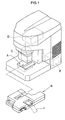
- Fig. 1 shows an appearance of a film scanner using a light-emitting diode (LED) light source unit according to the present invention
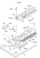
- Fig. 2 is an exploded view of this film scanner.
- the film scanner includes a light source unit A, a film carrier unit B, a lens unit C, a photoelectric converter unit D, and a control unit E.
- a beam from the light source unit A is irradiated on a developed photographic film F carried on the film carrier B and the transmission beam past this photographic film F is guided by the lens unit C to the photoelectric converter unit D.
- a CCD (Charge Coupled Device) type line sensor incorporated therein obtains, from an image in the photographic film F, image data in the form of digital signals corresponding to the three primary colors of R (red), G (green) and B (blue) and obtains also, by means of an infrared beam (IR), its beam intensity variable due to presence of a defect or flaw or dust or the like in the photographic film F as image data in the form of digital signals for use in flaw correction.
- IR infrared beam
- the light source unit A includes a plurality of light-emitting diode (LED) arrays (generically representing a green LED array G-LED, a blue LED array B-LED, and a red/infrared LED array R1 ⁇ R2 ⁇ IR-LED to be detailed later) each comprising an array of a plurality of LED elements 9 arranged along a main scanning direction for generating the beams of the three primary color components and the infrared beam.
- the film carrier unit B is designed for transporting the film F back and forth along a sub scanning direction. And, a plurality of film carrier units B are prepared to cope with a plurality of types of photographic films F such as 135 size, 240 size, 120/220 size films, so that these carriers are exchangeable.
- the lens unit C includes a zooming type optical lens which is operable to cause an image in the photographic film F carried by the film carrier B to be impinged in focus on the CCD type line sensor incorporated in the photoelectric converter unit D, the lens allowing variation of a magnifying power depending on the desired number of pixels to be obtained.
- the photoelectric converter unit D includes a three-line type CCD line sensor corresponding to the three primary colors of R (red), G (green) and B (blue) and a one-line type CCD line sensor having sensitivity for the infrared beam (IR).
- the light source unit A includes an upper case 10 formed as resin molded component and a lower case 20 formed of an aluminum alloy.
- the upper case 10 includes a flat upper table portion 11 and a box portion 12 formed integrally therewith and projecting from a bottom face of the upper table portion 11. Further, a resin cover 13 is provided for the bottom face of the upper table portion 11.
- the lower case 20 includes a bottom wall portion 21, a lateral wall portion 22 formed integrally therewith and a plurality of fins 23 as heat discharging elements formed integrally with respective outer faces of the bottom wall portion 21 and the lateral wall portion 22.
- This light source unit A further includes a pair of fans 24 for feeding cooling air to the fins 23.
- the upper table portion 11 of the upper case 10 defines an opening 11A of a predetermined width formed along the main scanning direction for irradiating beam upwards.
- a cylindrical condensing lens 30 and at a position below this condensing lens 30, there is provided an ND filter 31 movable into and out of the optical axis of the lens 30.
- this ND filter 31 is mounted to be slidable between a condition (position) where the filter is located downwardly of the condensing lens 30 and a further condition where the filter is retracted inside the cover 13.
- the filter 31 is operably connected with a crank mechanism 15 activated by a drive from an electromagnetic solenoid type actuator 14 in the cover 13.
- this ND filter 31 when this ND filter 31 is located at the position below the main condensing lens 30 for adjusting the CCD of the photoelectric converter unit D, the filter 31 reduces the amount of beam from the light source unit A, thus appropriately adjusting the photoelectric converter unit D with an appropriate amount of beam.
- the box portion 12 accommodates therein a first mirror M1 of dichroic type disposed at a lower position on an extension of the optical axis L of the condensing lens 30, a first lens Le1 of cylindrical type, a second mirror M2 of dichroic type disposed beside the first mirror M1, a second lens Le2 of cylindrical type for guiding beam to a reflecting side of the second mirror M2 and a third lens Le3 of cylindrical type for guiding the beam to a transmitting side of the second mirror M2.
- a first printed circuit board P1 mounting thereon a light-emitting diode array G-LED consisting of a plurality of chip-type green LED elements 9 linearly arranged along the main scanning direction and a light-emitting diode array B-LED consisting of a plurality of chip-type blue LED elements 9 linearly arranged along the main scanning direction.
- a second printed board P2 mounting thereon a light-emitting diode array R1 ⁇ R2 ⁇ IR-LED including first red, second red and infrared beam LED elements 9 linearly arranged in the mentioned order along the main scanning direction.
- the green LED array G-LED is disposed at the focal position of the first lens Le1
- the blue LED array B-LED is disposed at the focal position of the second lens Le2
- the first red, second red and infrared LED array R1 ⁇ R2 ⁇ IR-LED is disposed at the focal position of the third lens Le3, respectively.
- the green LED elements 9 have a wavelength of 400-480 nm, the blue LED elements 9 have a wavelength of 520-560 nm, and the first red LED elements 9 and the second red LED elements 9 have a combined wavelength of 620-750 nm, and the infrared LED elements 9 have a wavelength of 830-950 nm, respectively.
- the first mirror M1 transmits the beam of the particular wavelength (400-480 nm) from the green LED elements 9 while reflecting beams of any other wavelength.
- the second mirror M2 transmits the beams of the particular wavelengths (620-750 nm and 830-950 nm) from the first red, second red and infrared LED elements 9 while reflecting the beam from the blue LED elements 9 (520-560 nm).
- the beams from the green LED array G-LED are rendered into parallel rays through the first lens Le1 and then transmitted through the first mirror M1 to be guided to the condensing lens 30.
- the beams from the blue LED array B-LED are rendered into parallel rays through the second lens Le2 and reflected first by this second mirror M2 and then reflected by the first mirror M1 to be guided to the condensing lens 30.
- the beams from the first red, second red and infrared LED array R1 ⁇ R2 ⁇ IR-LED are rendered into parallel rays through the third lens Le3 and transmitted through the second mirror M2 and then reflected by the first mirror M1 to be guided to the condensing lens 30.
- positioning pins 17 are provided erect from the box portion 12 of the upper case 10 and positioning faces 18 are formed for coming into contact with the lens Le. Further, at portions of the box portion 12 facing the bottom wall portion 21 and the lateral wall portion 22, there are formed reference faces 19 for coming into contact with the printed circuit board P. At opposed ends of each lens Le (i.e.
- the first lens Le1, second lens Le2 or third lens Le3 there are integrally formed support pieces 33 for coming into contact with the positioning faces 18, pin holes 34 for engagement with the pins 17 and screw holes 36 through which fixing screws 35 are to be inserted.
- the construction for supporting the condensing lens 30 to the upper case 10 is identical to that for supporting the lenses Le to the box portion 12. Namely, the screws 35 will be inserted through the screw holes 36 formed in the support pieces 33 formed at the opposed ends of the condensing lens 30 and then the inserted screws 35 will be fixedly threaded with the upper case 10.
- the first printed circuit board P1 too defines pin holes 40 for engagement with the positioning pins 17.
- This first printed circuit board P1 will be fixed to the bottom wall portion 21 by means of screws 41 and the second printed circuit board P2 will be fixed in position to the lateral wall portion 22 by means of the screws 41 (see Fig. 2).
- silicon grease is applied to the interfaces thereof for improvement of heat conductivity.
- the positioning pins 17 formed on the bottom face of the box portion 12 will engage into the corresponding pin holes 40 of the first printed circuit board P1 supported to the bottom wall portion 21, thereby to fixedly determine the position relative to the first printed circuit board P1 and fixedly determine also the position of the lower case 20 relative to the upper case 10 at the same time.
- the position of the third lens Le3 relative to the second printed circuit board P2 too will be fixedly determined as well.
- the printed circuit board P uses a relatively thick aluminum substrate 45 as a material having a high heat conductivity.
- On this printed circuit board P as described hereinbefore, there are mounted the array of the chip type LED elements 9 along the main scanning direction. Further, on the surface of the printed circuit board P, there are also mounted a series of chip resistors CR along the extending direction of the array of the LED elements 9. These chip resistors CR all have a same resistance value and a same size. Heat generated when electric power is supplied to the chip resistors CR is conducted to the printed circuit board P and consequently to the LED elements 9, thereby to realize uniform temperature distribution among the plurality of LED elements 9.
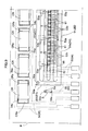
- Fig. 5 illustrates a manufacturing process of the printed circuit board P
- Fig. 6 illustrates a process of surface-mounting parts thereon. These processes are only illustrative, not limitative for the present invention.
- the surface of the substrate 45 which is formed of aluminum as described above is coated with a ceramic material for forming an insulating ceramic layer 46 (Fig. 5 (a) and Fig. 5 (b)).
- a printed circuit wiring (wiring land) W formed of a copper foil or a gold foil, etc. and a surface-mounting pad X are formed on the top face thereof.
- a resist film 47 made of an insulating resin is formed on the top surface of this printed circuit board P (Fig. 5 (d)).
- this printed circuit board P thus fabricated, there will be surface-mounted the LED elements 9 and a reflector unit 50 including a rectangular frame member 51 and reflectors 52 assembled integrally with each other.
- a pin-hole positioning arrangement similar to the one described above is employed also for mounting the reflector unit 50 to the printed circuit board P.
- a pair of reflector-side reference holes 50a are formed at two positions in the frame member 51 of the reflector unit 50 and a pair of board-side reference holes 40a are formed at corresponding positions in the printed circuit board P.
- the reflector unit 50 can be mounted at a predetermined position of the printed circuit board P in a reliable manner (Fig. 5 (e)).
- the mounting and positioning operation of the reflector unit 50 to the printed circuit board P can be effected by means of other type of arrangement (e.g. optical) using the board-side reference hole 40a of the printed circuit board P and the reflector-side reference holes 50a of the reflector unit 50.
- the unit 50 and the board P can be mounted together and fixed in position relative to each other by utilizing the pin holes 40 of the former and the reflector-side reference holes 50a of the latter.
- the bonding wire 61 is laid between the LED element 9 and the wiring land W, with the wire 61 leaping over the reflector 52 (Fig. 5 (f)).
- a flat face is formed on the top of the reflector 52 used in this embodiment.
- a relay land 52b is formed on this flat face.
- a first bonding wire portion 61a is laid between the LED element 9 and the relay land 52b and then a second bonding wire portion 61b is laid between the relay land 52b and the wiring land W (Fig. 6 (f)).
- Fig. 7 shows an appearance before the LED elements 9, the reflector unit 50 and others are surface-mounted on the printed circuit board P
- Fig. 8 shows an appearance after the surface-mounting
- Fig. 9 is a plan view showing the appearance after the surface-mounting.
- the resist layer 47 leaving a blank area greater than the area of the surface-mounting pad X so as to expose the ceramic layer 46.
- This ceramic layer 46 is formed by coating a ceramic material on the aluminum substrate 45 and has a much higher reflecting power than e.g. the resist layer 47.
- this ceramic layer 46 exposed outside the surface-mounting pad X functions as a back reflecting face for the beam emitted from the LED element 9 and contributes to increase of illumination intensity to the illuminated object (in this case, the photographic film F) by the LED array LED, in cooperation with reflecting faces 52a of the reflector unit 50 to be described later.
- a ceramic material having superior reflecting property as the insulating material to be coated on the surface of the metal substrate 45 or to select an appropriate coating method which provides a maximum mirror-like surface.
- the substrate 45 can be formed also of a copper plate or metal alloy or of a resin material.
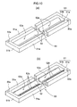
- the reflector unit 50 shown in Fig. 10 (a) is formed of a liquid crystalline polymer and consists essentially of a rectangular frame member 51 having an opposed pair of long-side portions 51a and an opposed pair of short-side portions 51b and two elongate reflectors 52.
- Each reflector 52 has a substantially right-triangular cross section and a length sufficient to substantially cover the entire length (main scanning direction length) of the LED array.
- Opposed terminal ends of this reflector 52 are joined to the opposed short-side portions 51b of the rectangular frame member 51 surrounding the circumference of the reflectors 52.
- Both the long-side portions 51a and the short-side portions 51b have a larger cross section than that of the reflector 52 and formed and joined together in the form of rectangle.
- Each reflector 52 includes the inclined reflecting face 52a which is to be located to face the LED elements 9 which the reflector 52 is surface-mounted on the board. This inclined reflecting face 52a reflects the beam from the LED elements 9 toward the object to be illuminated.
- Fig. 10 (b) shows a modification of the reflector unit 50.
- This unit differs from the reflector unit 50 shown in Fig.10 (a) in that the flat face is formed on the top of the reflector 52 and the above-described relay land 52b made of a conducting material such as copper is formed on this flat face.
- Fig. 11 which is a section of the area of the printed circuit board P surface-mounting the LED elements 9, the bonding wire 61 extending and connecting between the LED element 9 and the printed circuit wiring (wiring land) W is laid in such a manner that the wire 61 leaps over the reflector 52. And, the wiring land W is laid at an area or gap formed between the reflector 52 and the frame member 51 of the mounted reflector unit 50.
- the reflector 52 has a height of about 1 mm and the gap between the reflector 52 and the LED element 9 has a width of about 0.5 mm.
- the printed circuit wiring (wiring land) W includes a light-emitting wiring portion 53 for supplying power to the LED elements 9, a heating wiring portion 54 for supplying power to the chip resistors CR and a metering wiring portion 55 for applying a potential to a chip thermistor S acting as a temperature metering means.
- the LED array LED includes a plurality of units of LED elements 9, each unit consisting of seven LED elements 9 electrically serially connected to each other.
- the light emitting wiring portion 53 includes power terminals 53a each supplying power to one unit (group) of LED elements 9, and relay terminals 53b formed independently thereof along the array direction of the LED elements 9.
- the heating wiring portion 54 includes terminals 54a to be connected by solder 60 with opposed electrodes CRa of the chip resistors CR. Further, the metering wiring portion 55 includes terminals 55a which are connected by solder 60 with opposed electrodes Sa of the thermistor S.
- the light-emitting diode light source unit according to the present invention can be used also as a light source for use in an electrostatic copier, a flat bed scanner, etc.
Landscapes
- Engineering & Computer Science (AREA)
- Multimedia (AREA)
- Signal Processing (AREA)
- Microelectronics & Electronic Packaging (AREA)
- General Engineering & Computer Science (AREA)
- Optics & Photonics (AREA)
- Physics & Mathematics (AREA)
- Facsimile Scanning Arrangements (AREA)
- Led Device Packages (AREA)
- Light Sources And Details Of Projection-Printing Devices (AREA)
- Facsimile Heads (AREA)
- Printers Or Recording Devices Using Electromagnetic And Radiation Means (AREA)
- Structures For Mounting Electric Components On Printed Circuit Boards (AREA)
- Illuminated Signs And Luminous Advertising (AREA)
- Fastening Of Light Sources Or Lamp Holders (AREA)
Applications Claiming Priority (6)
| Application Number | Priority Date | Filing Date | Title |
|---|---|---|---|
| JP2003052629 | 2003-02-28 | ||
| JP2003052634 | 2003-02-28 | ||
| JP2003052629A JP3948417B2 (ja) | 2003-02-28 | 2003-02-28 | 光源ユニット |
| JP2003052632A JP2004265977A (ja) | 2003-02-28 | 2003-02-28 | 発光ダイオード光源ユニット |
| JP2003052634A JP2004265979A (ja) | 2003-02-28 | 2003-02-28 | 発光ダイオード光源ユニット |
| JP2003052632 | 2003-02-28 |
Publications (2)
| Publication Number | Publication Date |
|---|---|
| EP1453109A2 true EP1453109A2 (fr) | 2004-09-01 |
| EP1453109A3 EP1453109A3 (fr) | 2009-05-27 |
Family
ID=32776827
Family Applications (3)
| Application Number | Title | Priority Date | Filing Date |
|---|---|---|---|
| EP04004509A Withdrawn EP1453111A3 (fr) | 2003-02-28 | 2004-03-01 | Unité de sources lumineuses |
| EP04004506A Withdrawn EP1453109A3 (fr) | 2003-02-28 | 2004-03-01 | Unité de source lumineuse ayant des diodes émettrices de lumière |
| EP04004507A Withdrawn EP1453110A3 (fr) | 2003-02-28 | 2004-03-01 | Unité de source lumineuse ayant des diodes émettrices de lumière |
Family Applications Before (1)
| Application Number | Title | Priority Date | Filing Date |
|---|---|---|---|
| EP04004509A Withdrawn EP1453111A3 (fr) | 2003-02-28 | 2004-03-01 | Unité de sources lumineuses |
Family Applications After (1)
| Application Number | Title | Priority Date | Filing Date |
|---|---|---|---|
| EP04004507A Withdrawn EP1453110A3 (fr) | 2003-02-28 | 2004-03-01 | Unité de source lumineuse ayant des diodes émettrices de lumière |
Country Status (4)
| Country | Link |
|---|---|
| US (3) | US7018065B2 (fr) |
| EP (3) | EP1453111A3 (fr) |
| JP (3) | JP2004265979A (fr) |
| CN (3) | CN1306627C (fr) |
Families Citing this family (47)
| Publication number | Priority date | Publication date | Assignee | Title |
|---|---|---|---|---|
| JP2006147999A (ja) * | 2004-11-24 | 2006-06-08 | Kyocera Corp | 発光素子用配線基板並びに発光装置 |
| US7361938B2 (en) * | 2004-06-03 | 2008-04-22 | Philips Lumileds Lighting Company Llc | Luminescent ceramic for a light emitting device |
| TW200605169A (en) * | 2004-06-29 | 2006-02-01 | Sanyo Electric Co | Circuit device and process for manufacture thereof |
| WO2006032160A1 (fr) | 2004-09-21 | 2006-03-30 | Volpi Ag | Source d'eclairage |
| KR100638047B1 (ko) * | 2004-10-15 | 2006-10-23 | 엘지전자 주식회사 | 백라이트 유닛을 갖는 액정 디스플레이 |
| US8541797B2 (en) * | 2004-11-18 | 2013-09-24 | Koninklijke Philips N.V. | Illuminator and method for producing such illuminator |
| JP4241658B2 (ja) | 2005-04-14 | 2009-03-18 | シチズン電子株式会社 | 発光ダイオード光源ユニット及びそれを用いて形成した発光ダイオード光源 |
| JPWO2007023807A1 (ja) * | 2005-08-23 | 2009-02-26 | 株式会社東芝 | 発光装置とそれを用いたバックライトおよび液晶表示装置 |
| US7470921B2 (en) * | 2005-09-20 | 2008-12-30 | Summit Business Products, Inc. | Light-emitting diode device |
| US8251689B2 (en) * | 2005-09-20 | 2012-08-28 | Summit Business Products, Inc. | Ultraviolet light-emitting diode device |
| JP4965858B2 (ja) * | 2005-12-26 | 2012-07-04 | 株式会社東芝 | レンズ付発光ダイオード装置 |
| DE102006015510A1 (de) * | 2006-03-31 | 2007-10-11 | Compal Communications Inc. | Leuchtanordnung |
| JP4840648B2 (ja) * | 2006-04-03 | 2011-12-21 | Nkワークス株式会社 | フィルムスキャナ |
| US20080019142A1 (en) * | 2006-06-29 | 2008-01-24 | Thomas & Betts International, Inc. | Lamp assembly adapted to illuminate a backlit sign |
| US7738235B2 (en) * | 2006-07-31 | 2010-06-15 | B/E Aerospace, Inc. | LED light apparatus |
| CN100423257C (zh) * | 2006-12-20 | 2008-10-01 | 黄虎钧 | 具有发光二极管晶片的发光棒 |
| JP5066953B2 (ja) * | 2007-03-07 | 2012-11-07 | 富士ゼロックス株式会社 | 露光装置および画像形成装置 |
| US7959282B2 (en) * | 2007-12-20 | 2011-06-14 | Summit Business Products, Inc. | Concentrated energy source |
| US20090167854A1 (en) * | 2007-12-26 | 2009-07-02 | Crs Electronic Co., Ltd. | Apparatus For Converting Film Images Into Digital Data |
| US20090167853A1 (en) * | 2007-12-26 | 2009-07-02 | Crs Electronic Co., Ltd | Apparatus For Converting Film Images Into Digital Data |
| US8049237B2 (en) | 2007-12-28 | 2011-11-01 | Nichia Corporation | Light emitting device |
| US8115974B2 (en) * | 2008-01-14 | 2012-02-14 | Crs Electronic Co., Ltd. | Device to transfer photo images into digital data |
| US7940326B2 (en) * | 2008-01-14 | 2011-05-10 | Crs Electronic Co., Ltd. | Device to transfer photo images into digital data |
| CN101493214B (zh) * | 2008-01-23 | 2011-02-02 | 环隆电气股份有限公司 | 具有高密度电性连接的多波长发光模块 |
| US20110095310A1 (en) * | 2008-03-26 | 2011-04-28 | Shimane Prefectural Government | Semiconductor light emitting module and method of manufacturing the same |
| US20090257096A1 (en) * | 2008-04-10 | 2009-10-15 | Crs Electronic Co., Ltd | Apparatus With Display For Converting Photographs Into Digital Data |
| JP2010238604A (ja) * | 2009-03-31 | 2010-10-21 | Koito Mfg Co Ltd | 発光素子モジュール化部材および灯具ユニット |
| TW201103170A (en) * | 2009-07-08 | 2011-01-16 | Paragon Sc Lighting Tech Co | LED package structure with concave area for positioning heat-conducting substance and method for manufacturing the same |
| US8998442B2 (en) | 2009-11-12 | 2015-04-07 | Sharp Kabushiki Kaisha | Lighting device, display device and television receiver |
| KR20110080061A (ko) * | 2010-01-04 | 2011-07-12 | 삼성엘이디 주식회사 | 항만 조명장치 |
| JP5421799B2 (ja) * | 2010-01-18 | 2014-02-19 | パナソニック株式会社 | Ledユニット |
| US8729781B2 (en) * | 2010-03-03 | 2014-05-20 | Koninklijke Philips N.V. | Electric lamp having reflector for transferring heat from light source |
| KR101883839B1 (ko) * | 2010-12-07 | 2018-08-30 | 엘지이노텍 주식회사 | 발광소자 모듈 및 이를 포함하는 백라이트 유닛 |
| US8997732B2 (en) * | 2010-12-15 | 2015-04-07 | General Electric Company | Method and apparatus for the thermal protection of LED light modules in a range hood appliance |
| JP5723841B2 (ja) * | 2012-09-11 | 2015-05-27 | 京セラドキュメントソリューションズ株式会社 | 画像読取装置及びそれを備えた画像形成装置 |
| CN103929883B (zh) * | 2013-01-15 | 2017-01-25 | 南京尚孚电子电路有限公司 | 一种单晶cob封装碗杯孔状铝基板的制作方法 |
| JP2014158015A (ja) * | 2013-01-15 | 2014-08-28 | Rohm Co Ltd | 半導体装置 |
| CN103529635B (zh) * | 2013-10-16 | 2016-05-04 | 北京大学东莞光电研究院 | 一种数码彩扩机引擎片夹led平面光源 |
| US11049725B1 (en) * | 2014-05-29 | 2021-06-29 | Corporation For National Research Initiatives | Method for etching deep, high-aspect ratio features into silicon carbide and gallium nitride |
| CN104105348A (zh) * | 2014-06-16 | 2014-10-15 | 张龙 | 一种铝基板加工工艺 |
| US9976844B2 (en) * | 2015-02-06 | 2018-05-22 | Medlumics S.L. | Miniaturized OCT package and assembly thereof |
| JP2017021988A (ja) * | 2015-07-10 | 2017-01-26 | 東芝ライテック株式会社 | 車両用発光装置、車両用照明装置および車両用灯具 |
| JP6422031B2 (ja) * | 2015-07-30 | 2018-11-14 | 京セラドキュメントソリューションズ株式会社 | 照明装置、画像読取装置及び画像形成装置 |
| JP2019197610A (ja) * | 2018-05-07 | 2019-11-14 | 株式会社小糸製作所 | 照明装置 |
| US10801697B2 (en) * | 2018-11-20 | 2020-10-13 | Luxmux Technology Corporation | Broadband light source module combining spectrums of different types of light sources |
| KR102700062B1 (ko) * | 2018-12-21 | 2024-08-29 | 엘지이노텍 주식회사 | 액체 렌즈를 포함하는 카메라 모듈 및 그의 제어 방법 |
| JP2022051125A (ja) * | 2020-09-18 | 2022-03-31 | 日亜化学工業株式会社 | 発光装置 |
Family Cites Families (46)
| Publication number | Priority date | Publication date | Assignee | Title |
|---|---|---|---|---|
| US4000437A (en) * | 1975-12-17 | 1976-12-28 | Integrated Display Systems Incorporated | Electric display device |
| JPS59146069A (ja) * | 1983-02-08 | 1984-08-21 | Canon Inc | 光源安定化装置 |
| JPS6089988A (ja) * | 1983-10-24 | 1985-05-20 | Toshiba Corp | 複写機用ledアレイ光源 |
| JPS6184880A (ja) * | 1984-10-02 | 1986-04-30 | Sharp Corp | 固体発光表示装置 |
| JPH0680841B2 (ja) * | 1986-04-07 | 1994-10-12 | 株式会社小糸製作所 | 照明装置 |
| JPH0821747B2 (ja) * | 1987-04-23 | 1996-03-04 | 日本電気株式会社 | 光伝送装置 |
| KR880014692A (ko) * | 1987-05-30 | 1988-12-24 | 강진구 | 반사경이 부착된 반도체 발광장치 |
| US4881237A (en) * | 1988-08-26 | 1989-11-14 | Massachusetts Institute Of Technology | Hybrid two-dimensional surface-emitting laser arrays |
| US4896168A (en) * | 1988-08-30 | 1990-01-23 | Eastman Kodak Company | Light emitting diode printhead |
| US5150016A (en) * | 1990-09-21 | 1992-09-22 | Rohm Co., Ltd. | LED light source with easily adjustable luminous energy |
| US5119174A (en) * | 1990-10-26 | 1992-06-02 | Chen Der Jong | Light emitting diode display with PCB base |
| JP2772166B2 (ja) * | 1991-07-25 | 1998-07-02 | ローム株式会社 | Led光源装置 |
| US5226723A (en) * | 1992-05-11 | 1993-07-13 | Chen Der Jong | Light emitting diode display |
| JPH06291939A (ja) | 1993-03-30 | 1994-10-18 | Toshiba Lighting & Technol Corp | Led光源装置、読取装置および読取装置組込機器 |
| JP3219263B2 (ja) * | 1995-05-23 | 2001-10-15 | キヤノン株式会社 | 発光装置 |
| JP3185204B2 (ja) * | 1995-05-31 | 2001-07-09 | 日本精機株式会社 | 発光素子アセンブリ |
| DE19549818B4 (de) * | 1995-09-29 | 2010-03-18 | Osram Opto Semiconductors Gmbh | Optoelektronisches Halbleiter-Bauelement |
| JP3158037B2 (ja) * | 1996-02-29 | 2001-04-23 | 三菱電機株式会社 | 記録装置および記録方法 |
| JP3488570B2 (ja) * | 1996-03-29 | 2004-01-19 | ローム株式会社 | Led発光装置およびこれを用いた面発光照明装置 |
| JPH10129344A (ja) * | 1996-10-28 | 1998-05-19 | Katsuo Inoue | 字光式ナンバープレート |
| US6583444B2 (en) * | 1997-02-18 | 2003-06-24 | Tessera, Inc. | Semiconductor packages having light-sensitive chips |
| EP0863422B1 (fr) * | 1997-03-04 | 2006-10-04 | Matsushita Electric Industrial Co., Ltd. | Dispositif d'illumination linéaire |
| JPH10275957A (ja) * | 1997-03-31 | 1998-10-13 | Hitachi Ltd | 光半導体チップキャリア |
| US6183100B1 (en) * | 1997-10-17 | 2001-02-06 | Truck-Lite Co., Inc. | Light emitting diode 360° warning lamp |
| US6385222B1 (en) * | 1998-11-19 | 2002-05-07 | The Furukawa Electric Co., Ltd. | Semiconductor laser module, and method for driving the semiconductor laser module |
| JP2000281240A (ja) * | 1999-03-30 | 2000-10-10 | Seiko Epson Corp | 画像形成装置 |
| WO2000079605A1 (fr) * | 1999-06-23 | 2000-12-28 | Citizen Electronics Co., Ltd. | Diode électroluminescente |
| JP2001045225A (ja) * | 1999-07-26 | 2001-02-16 | Fuji Photo Film Co Ltd | 画像読取装置 |
| WO2001029904A1 (fr) * | 1999-10-18 | 2001-04-26 | Obschestvo S Ogranichennoi Otvetstvennostiju 'korvet-Lights' | Diode a luminescence |
| DE10020465A1 (de) * | 2000-04-26 | 2001-11-08 | Osram Opto Semiconductors Gmbh | Strahlungsemittierendes Halbleiterbauelement mit Lumineszenzkonversionselement |
| JP4926337B2 (ja) * | 2000-06-28 | 2012-05-09 | アバゴ・テクノロジーズ・ジェネラル・アイピー(シンガポール)プライベート・リミテッド | 光源 |
| JP4432275B2 (ja) * | 2000-07-13 | 2010-03-17 | パナソニック電工株式会社 | 光源装置 |
| EP1179858B1 (fr) * | 2000-08-09 | 2009-03-18 | Avago Technologies General IP (Singapore) Pte. Ltd | Dispositifs émetteurs de lumière |
| EP1187226B1 (fr) * | 2000-09-01 | 2012-12-26 | Citizen Electronics Co., Ltd. | LED pour montage en surface et son procédé de fabrication |
| TW521409B (en) * | 2000-10-06 | 2003-02-21 | Shing Chen | Package of LED |
| JP2002281240A (ja) | 2001-03-14 | 2002-09-27 | Canon Inc | 画像読み取り装置 |
| ATE425556T1 (de) * | 2001-04-12 | 2009-03-15 | Matsushita Electric Works Ltd | Lichtquellenbauelement mit led und verfahren zu seiner herstellung |
| JP3891115B2 (ja) * | 2001-04-17 | 2007-03-14 | 日亜化学工業株式会社 | 発光装置 |
| DE10122002A1 (de) * | 2001-05-07 | 2002-11-21 | Osram Opto Semiconductors Gmbh | Gehäuse für ein optoelektronisches Bauelement und optoelektronisches Bauelement |
| JP3844196B2 (ja) * | 2001-06-12 | 2006-11-08 | シチズン電子株式会社 | 発光ダイオードの製造方法 |
| JP3891400B2 (ja) * | 2001-07-25 | 2007-03-14 | シチズン電子株式会社 | 発光ダイオード |
| JP4045781B2 (ja) * | 2001-08-28 | 2008-02-13 | 松下電工株式会社 | 発光装置 |
| US6480389B1 (en) * | 2002-01-04 | 2002-11-12 | Opto Tech Corporation | Heat dissipation structure for solid-state light emitting device package |
| US6851831B2 (en) * | 2002-04-16 | 2005-02-08 | Gelcore Llc | Close packing LED assembly with versatile interconnect architecture |
| US6964501B2 (en) * | 2002-12-24 | 2005-11-15 | Altman Stage Lighting Co., Ltd. | Peltier-cooled LED lighting assembly |
| EP1448031A1 (fr) * | 2003-02-13 | 2004-08-18 | Yang, Pi-Fu | Carte électronique avec des évidements concaves pour une diode électroluminescente et le procédé de fabrication |
-
2003
- 2003-02-28 JP JP2003052634A patent/JP2004265979A/ja active Pending
- 2003-02-28 JP JP2003052632A patent/JP2004265977A/ja active Pending
- 2003-02-28 JP JP2003052629A patent/JP3948417B2/ja not_active Expired - Fee Related
-
2004
- 2004-02-17 CN CNB2004100052619A patent/CN1306627C/zh not_active Expired - Fee Related
- 2004-02-19 CN CNB2004100054987A patent/CN100338787C/zh not_active Expired - Fee Related
- 2004-02-19 CN CNB2004100055000A patent/CN100344003C/zh not_active Expired - Fee Related
- 2004-02-27 US US10/789,089 patent/US7018065B2/en not_active Expired - Fee Related
- 2004-02-27 US US10/789,003 patent/US7108399B2/en not_active Expired - Fee Related
- 2004-02-27 US US10/789,088 patent/US7204609B2/en not_active Expired - Fee Related
- 2004-03-01 EP EP04004509A patent/EP1453111A3/fr not_active Withdrawn
- 2004-03-01 EP EP04004506A patent/EP1453109A3/fr not_active Withdrawn
- 2004-03-01 EP EP04004507A patent/EP1453110A3/fr not_active Withdrawn
Also Published As
| Publication number | Publication date |
|---|---|
| CN1525581A (zh) | 2004-09-01 |
| CN1525580A (zh) | 2004-09-01 |
| EP1453110A2 (fr) | 2004-09-01 |
| EP1453110A3 (fr) | 2009-05-27 |
| JP3948417B2 (ja) | 2007-07-25 |
| US7204609B2 (en) | 2007-04-17 |
| JP2004265979A (ja) | 2004-09-24 |
| US20040179373A1 (en) | 2004-09-16 |
| EP1453109A3 (fr) | 2009-05-27 |
| US20040179359A1 (en) | 2004-09-16 |
| EP1453111A3 (fr) | 2009-06-03 |
| US20040170019A1 (en) | 2004-09-02 |
| CN100338787C (zh) | 2007-09-19 |
| CN1306627C (zh) | 2007-03-21 |
| JP2004265977A (ja) | 2004-09-24 |
| US7018065B2 (en) | 2006-03-28 |
| US7108399B2 (en) | 2006-09-19 |
| JP2004266412A (ja) | 2004-09-24 |
| CN100344003C (zh) | 2007-10-17 |
| CN1525579A (zh) | 2004-09-01 |
| EP1453111A2 (fr) | 2004-09-01 |
Similar Documents
| Publication | Publication Date | Title |
|---|---|---|
| US7204609B2 (en) | Light-emitting diode light source unit | |
| US7626774B2 (en) | Solid-state imaging device and electronic device including same | |
| US6294776B2 (en) | Integrated optical imaging assembly | |
| JP2009086488A (ja) | 線状光源装置、およびイメージセンサモジュール | |
| CN1153441C (zh) | 线光源及图像输入装置 | |
| JP3666969B2 (ja) | 画像読取装置及び光源ユニット | |
| JP2004349628A (ja) | 半導体発光装置及びそれを用いた撮影用照明装置 | |
| JPH09246602A (ja) | 発光ダイオード整列光源 | |
| JPH11215302A (ja) | 画像読み取り装置および樹脂パッケージ型光源 | |
| JPH1175019A (ja) | 光源装置及び画像読取装置 | |
| JPH09330611A (ja) | 画像読取装置及び光源ユニット | |
| JP4069416B2 (ja) | 発光ダイオード光源ユニット | |
| JP2008005465A (ja) | イメージセンサ装置、画像読取装置および画像形成装置 | |
| JP2004265980A (ja) | 発光ダイオード光源ユニット | |
| US20150334259A1 (en) | Circuit board, image sensor unit, image reading apparatus, and image forming apparatus | |
| JPH11215304A (ja) | 画像読み取り装置用駆動部品ユニットの製造方法、画像読み取り装置用駆動部品ユニット中間品、画像読み取り装置用駆動部品ユニット、およびそれを備えた画像読み取り装置 | |
| JP3146401B2 (ja) | イメージセンサ | |
| JP3879926B2 (ja) | フィルムスキャナ | |
| JPH10190945A (ja) | 密着型イメージセンサ | |
| JPH10285331A (ja) | イメージセンサおよびこのイメージセンサを用いた情報処理装置 | |
| JP2000083138A (ja) | イメ―ジ読取装置とそのための発光アレイ | |
| JP2016197752A (ja) | 回路基板、イメージセンサユニット、画像読取装置および画像形成装置 | |
| JPH07250213A (ja) | 画像読取装置 | |
| JPH10177639A (ja) | イメージセンサー | |
| JPH0470363A (ja) | 光書き込みヘッド |
Legal Events
| Date | Code | Title | Description |
|---|---|---|---|
| PUAI | Public reference made under article 153(3) epc to a published international application that has entered the european phase |
Free format text: ORIGINAL CODE: 0009012 |
|
| AK | Designated contracting states |
Kind code of ref document: A2 Designated state(s): AT BE BG CH CY CZ DE DK EE ES FI FR GB GR HU IE IT LI LU MC NL PL PT RO SE SI SK TR |
|
| AX | Request for extension of the european patent |
Extension state: AL LT LV MK |
|
| PUAL | Search report despatched |
Free format text: ORIGINAL CODE: 0009013 |
|
| AK | Designated contracting states |
Kind code of ref document: A3 Designated state(s): AT BE BG CH CY CZ DE DK EE ES FI FR GB GR HU IE IT LI LU MC NL PL PT RO SE SI SK TR |
|
| AX | Request for extension of the european patent |
Extension state: AL LT LV MK |
|
| 17P | Request for examination filed |
Effective date: 20090724 |
|
| AKX | Designation fees paid |
Designated state(s): DE FR GB |
|
| STAA | Information on the status of an ep patent application or granted ep patent |
Free format text: STATUS: THE APPLICATION HAS BEEN WITHDRAWN |
|
| 18W | Application withdrawn |
Effective date: 20110129 |