EP1456034B1 - Niederspannungs-tintenstrahlmodul - Google Patents
Niederspannungs-tintenstrahlmodul Download PDFInfo
- Publication number
- EP1456034B1 EP1456034B1 EP02799941A EP02799941A EP1456034B1 EP 1456034 B1 EP1456034 B1 EP 1456034B1 EP 02799941 A EP02799941 A EP 02799941A EP 02799941 A EP02799941 A EP 02799941A EP 1456034 B1 EP1456034 B1 EP 1456034B1
- Authority
- EP
- European Patent Office
- Prior art keywords
- piezoelectric element
- ink
- chamber
- jet printing
- printing module
- Prior art date
- Legal status (The legal status is an assumption and is not a legal conclusion. Google has not performed a legal analysis and makes no representation as to the accuracy of the status listed.)
- Expired - Lifetime
Links
- 238000007641 inkjet printing Methods 0.000 title claims abstract description 30
- 238000000034 method Methods 0.000 claims description 9
- HFGPZNIAWCZYJU-UHFFFAOYSA-N lead zirconate titanate Chemical compound [O-2].[O-2].[O-2].[O-2].[O-2].[Ti+4].[Zr+4].[Pb+2] HFGPZNIAWCZYJU-UHFFFAOYSA-N 0.000 claims description 7
- 238000000151 deposition Methods 0.000 claims description 4
- 230000004913 activation Effects 0.000 claims 1
- 238000004519 manufacturing process Methods 0.000 abstract 1
- 238000005086 pumping Methods 0.000 description 21
- 230000000052 comparative effect Effects 0.000 description 6
- 230000005684 electric field Effects 0.000 description 5
- 239000000463 material Substances 0.000 description 5
- 238000010586 diagram Methods 0.000 description 4
- 238000006073 displacement reaction Methods 0.000 description 4
- 229910000833 kovar Inorganic materials 0.000 description 4
- 239000011230 binding agent Substances 0.000 description 2
- 239000000919 ceramic Substances 0.000 description 2
- 239000010408 film Substances 0.000 description 2
- 238000001746 injection moulding Methods 0.000 description 2
- 229910052751 metal Inorganic materials 0.000 description 2
- 239000002184 metal Substances 0.000 description 2
- 239000000203 mixture Substances 0.000 description 2
- 239000000843 powder Substances 0.000 description 2
- 239000000758 substrate Substances 0.000 description 2
- OKTJSMMVPCPJKN-UHFFFAOYSA-N Carbon Chemical compound [C] OKTJSMMVPCPJKN-UHFFFAOYSA-N 0.000 description 1
- 229910000531 Co alloy Inorganic materials 0.000 description 1
- RYGMFSIKBFXOCR-UHFFFAOYSA-N Copper Chemical compound [Cu] RYGMFSIKBFXOCR-UHFFFAOYSA-N 0.000 description 1
- KGWWEXORQXHJJQ-UHFFFAOYSA-N [Fe].[Co].[Ni] Chemical compound [Fe].[Co].[Ni] KGWWEXORQXHJJQ-UHFFFAOYSA-N 0.000 description 1
- 229910052782 aluminium Inorganic materials 0.000 description 1
- XAGFODPZIPBFFR-UHFFFAOYSA-N aluminium Chemical compound [Al] XAGFODPZIPBFFR-UHFFFAOYSA-N 0.000 description 1
- 229910052799 carbon Inorganic materials 0.000 description 1
- 239000004020 conductor Substances 0.000 description 1
- 230000008602 contraction Effects 0.000 description 1
- 229910052802 copper Inorganic materials 0.000 description 1
- 239000010949 copper Substances 0.000 description 1
- 230000001419 dependent effect Effects 0.000 description 1
- 238000005530 etching Methods 0.000 description 1
- PCHJSUWPFVWCPO-UHFFFAOYSA-N gold Chemical compound [Au] PCHJSUWPFVWCPO-UHFFFAOYSA-N 0.000 description 1
- 239000010931 gold Substances 0.000 description 1
- 229910052737 gold Inorganic materials 0.000 description 1
- 238000002347 injection Methods 0.000 description 1
- 239000007924 injection Substances 0.000 description 1
- 150000002739 metals Chemical class 0.000 description 1
- -1 nickel-chrome Chemical compound 0.000 description 1
- 239000002243 precursor Substances 0.000 description 1
- 238000007639 printing Methods 0.000 description 1
- 230000000284 resting effect Effects 0.000 description 1
- 239000010409 thin film Substances 0.000 description 1
- MAKDTFFYCIMFQP-UHFFFAOYSA-N titanium tungsten Chemical compound [Ti].[W] MAKDTFFYCIMFQP-UHFFFAOYSA-N 0.000 description 1
Images


Classifications
-
- B—PERFORMING OPERATIONS; TRANSPORTING
- B41—PRINTING; LINING MACHINES; TYPEWRITERS; STAMPS
- B41J—TYPEWRITERS; SELECTIVE PRINTING MECHANISMS, i.e. MECHANISMS PRINTING OTHERWISE THAN FROM A FORME; CORRECTION OF TYPOGRAPHICAL ERRORS
- B41J2/00—Typewriters or selective printing mechanisms characterised by the printing or marking process for which they are designed
- B41J2/005—Typewriters or selective printing mechanisms characterised by the printing or marking process for which they are designed characterised by bringing liquid or particles selectively into contact with a printing material
- B41J2/01—Ink jet
- B41J2/135—Nozzles
- B41J2/16—Production of nozzles
- B41J2/1621—Manufacturing processes
- B41J2/1637—Manufacturing processes molding
-
- B—PERFORMING OPERATIONS; TRANSPORTING
- B41—PRINTING; LINING MACHINES; TYPEWRITERS; STAMPS
- B41J—TYPEWRITERS; SELECTIVE PRINTING MECHANISMS, i.e. MECHANISMS PRINTING OTHERWISE THAN FROM A FORME; CORRECTION OF TYPOGRAPHICAL ERRORS
- B41J2/00—Typewriters or selective printing mechanisms characterised by the printing or marking process for which they are designed
- B41J2/005—Typewriters or selective printing mechanisms characterised by the printing or marking process for which they are designed characterised by bringing liquid or particles selectively into contact with a printing material
- B41J2/01—Ink jet
- B41J2/135—Nozzles
- B41J2/16—Production of nozzles
- B41J2/1607—Production of print heads with piezoelectric elements
- B41J2/161—Production of print heads with piezoelectric elements of film type, deformed by bending and disposed on a diaphragm
-
- B—PERFORMING OPERATIONS; TRANSPORTING
- B41—PRINTING; LINING MACHINES; TYPEWRITERS; STAMPS
- B41J—TYPEWRITERS; SELECTIVE PRINTING MECHANISMS, i.e. MECHANISMS PRINTING OTHERWISE THAN FROM A FORME; CORRECTION OF TYPOGRAPHICAL ERRORS
- B41J2202/00—Embodiments of or processes related to ink-jet or thermal heads
- B41J2202/01—Embodiments of or processes related to ink-jet heads
- B41J2202/03—Specific materials used
-
- B—PERFORMING OPERATIONS; TRANSPORTING
- B41—PRINTING; LINING MACHINES; TYPEWRITERS; STAMPS
- B41J—TYPEWRITERS; SELECTIVE PRINTING MECHANISMS, i.e. MECHANISMS PRINTING OTHERWISE THAN FROM A FORME; CORRECTION OF TYPOGRAPHICAL ERRORS
- B41J2202/00—Embodiments of or processes related to ink-jet or thermal heads
- B41J2202/01—Embodiments of or processes related to ink-jet heads
- B41J2202/11—Embodiments of or processes related to ink-jet heads characterised by specific geometrical characteristics
Definitions
- This invention relates to a method of depositing ink and an ink jet printing module.
- An ink jet printing module ejects ink from an orifice in the direction of a substrate.
- the ink can be ejected as a series of droplets generated by a piezoelectric ink jet printing module.
- An example of a particular printing module can have 256 jets in four groups of 64 jets each.
- a piezoelectric ink jet printing module can include a module body, a piezoelectric element, and electrical contacts that drive the piezoelectric element.
- the module body is a rectangular member into the surfaces of which are machined a series of ink chambers that serve as pumping chambers for the ink.
- the piezoelectric element can be disposed over the surface of the body to cover the pumping chambers in a manner to pressurize the ink in the pumping chambers to eject the ink.
- US 6,217,158 B1 is directed to a piezoelectric vibrator unit including an elastic plate made of piezoelectric material having at least one curved portion.
- the piezoelectric vibrator unit also includes at least one common electrode and a discrete electrode which are formed on opposite sides of the elastic plate. The application of an electric field applied between the two electrodes causes the extension or contraction of the curved portion of the plate.
- the aim of the present invention is to provide an improved method for depositing ink and an improved ink jet printing module. This is achieved according to the invention by the method of claim 1 and the module of claim 5.
- the dependent claims contain preferred embodiments.
- An ink jet printing module includes a piezoelectric element positioned over jetting regions of a body.
- the jetting regions can be portions of pumping chambers within the body.
- the pumping chambers can be sealed.
- Electrical contacts, such as electrodes, can be positioned on a surface of the piezoelectric element.
- the piezoelectric element spans each jetting region. When a voltage is applied to an electrical contact, the shape of the piezoelectric element changes in a jetting region, thereby subjecting the ink within the corresponding pumping chamber to jetting pressure.
- the ink is ejected from the pumping chamber and deposited on a substrate.
- piezoelectric ink jet printing module is a shear mode module, such as the module described in U.S. Patent No. 5,640,184 , the entire contents of which is incorporated herein by reference.
- the electrical contacts in a shear mode module can be located on the side of the piezoelectric element adjacent to the ink chamber.
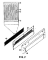
- piezoelectric ink jet head 2 includes one or more modules 4 which are assembled into collar element 10 to which is attached manifold plate 12 and orifice plate 14. Ink is introduced into module 4 through collar 10. Module 4 is actuated to eject ink from orifices 16 on orifice plate 14.
- Ink jet printing module 4 includes body 20, which can be made from materials such as sintered carbon or a ceramic.
- a plurality of chambers 22 are machined or otherwise manufactured into body 20 to form pumping chambers.
- Ink passes through ink fill passage 26, which is also machined into body 20, to fill the pumping chambers.
- Opposing surfaces of body 4 include a series of electrical contacts 31 and 31' arranged to be positioned over the pumping chambers in body 20. Electrical contacts 31 and 31' are connected to leads, which, in turn, can be connected to integrated circuits 33 and 33'. The components are sealed together to form the print module.
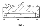
- piezoelectric element 34 has electrodes 40 on one surface of the piezoelectric element 34. Electrodes 40 register with electrical contacts 31, allowing the electrodes to be individually addressed by a driver integrated circuit. Electrodes 40 can be formed by chemically etching away conductive metal that has been deposited onto the surface of the piezoelectric element. Suitable methods of forming electrodes are also described in U.S. Patent No. 6,037,707 , which is herein incorporated by reference in its entirety. The electrode can be formed of conductors such as copper, aluminum, titanium-tungsten, nickel-chrome, or gold. Each electrode 40 is placed and sized to correspond to a chamber 22 in body 4 to form a pumping chamber.
- Each electrode 40 has elongated region 42, having a length and width slightly narrower than the dimensions of the pumping chamber such that gap 43 exists between the perimeter of electrodes 40 and the sides and end of the pumping chamber.
- These electrode regions 42 which are centered on the pumping chambers, are the drive electrodes that cover a jetting region of piezoelectric element 34.
- a second electrode 52 on piezoelectric element 34 generally corresponds to the area of body 20 outside chamber 22, and, accordingly, outside the pumping chamber.
- Electrode 52 is the common (ground) electrode.
- Electrode 52 can be comb-shaped (as shown) or can be individually addressable electrode strips. The film electrodes and piezoelectric element electrodes overlap sufficiently for good electrical contact and easy alignment of the film and the piezoelectric element.
- the piezoelectric element can be a single monolithic lead zirconium titanate (PZT) member.
- the piezoelectric element drives the ink from the pumping chambers by displacement induced by an applied voltage.
- the displacement is a function of, in part, the poling of the material.
- the piezoelectric element is poled by the application of an electric field.
- a poling process is described, for example, in U.S. Patent No. 5,605,659 , which is herein incorporated by reference in its entirety.
- the degree of poling can depend on the strength and duration of the applied electric field. When the poling voltage is removed, the piezoelectric domains are aligned.
- the piezoelectric element can have a thickness of 5 to 300 microns, 10 to 250 microns, 15 to 150 microns, less than 100 microns, or less than 50 microns.
- the piezoelectric element can be stiffened, for example, by introducing a curved surface in a portion of the element that covers the ink chamber.
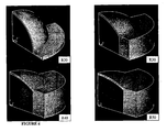
- the curved surface can have a substantially constant curvature, such as a spherical or cylindrical shape. Referring to FIG. 3 , a region 100 of piezoelectric element 34 is curved.
- the curvature of the piezoelectric element 34 is concave relative to ink chamber 102.
- the concave curvature of the surface can reduce buckling that otherwise may occur during jetting.
- Walls 104 of the chamber 102 can be oriented to contact the stiffened piezoelectric element 34 at an angle of greater than ninety degrees.
- the chamber can have a width of less than 1200 microns, a width of 50 to 1000 microns, or a width of 100 to 800 microns. Electrodes 42 and 52 are on surface 106 of the piezoelectric element 34. By applying a jetting voltage across the electrodes, ink within the chamber is subjected to a jetting pressure, which deposits ink from an exit orifice of the ink chamber.
- the jetting voltage can be less than 60 volts.
- the curved surface has a substantially constant radius of curvature.
- the degree of curvature, or radius of curvature affects the stiffness and jetting characteristics of the module.
- the radius of curvature is the radius of a circle drawn to encompass the curved surface.
- the curved surface can have a radius of curvature of less than 5 millimeters, or less than 3 millimeters.
- the curved surface can have a radius of curvature of 500 to 3000 microns, 1000 to 2800 microns, or 1500 to 2600 microns.
- the curved surface has a spherical shape.
- the ink jet printing module can be prepared by forming a stiffened piezoelectric element, and positioning the piezoelectric element over an ink chamber to subject ink within the chamber to a jetting pressure upon applying a jetting voltage.
- the stiffened piezoelectric element can be prepared by grinding a curved surface into a thin layer of piezoelectric material or by injection molding a precursor into a mold having the curved surface features of the piezoelectric element.
- a mixture can be prepared from a piezoelectric material powder and an organic binder. The mixture is injection molded to form a green sheet, which can be heated to remove the binder.
- the green sheet can be a thin film having a thickness of 10 to 50 microns, or 20 to 40 microns.
- the powder can be sintered, for example, to at least about 95% of theoretical density. Injection molding to form a piezoelectric article is described, for example, in U.S. Patent No. 5,340,510 , which is incorporated by reference in its entirety.
- the curvature stiffens the piezoelectric element and improves jetting of ink when a low voltage is applied to the element.
- a comparable ink jet printing module having a flat piezoelectric element requires application of a higher voltage to jet an ink drop of comparable volume.
- a concave surface relative to the chamber can lead to higher positive pressure within the chamber than negative pressure during jetting, for example, a pressure during jetting that can be up to two times higher the pressure during chamber filling. Reducing the dimensions of the ink jet printing module can also lead to higher voltage requirements to achieve a given drop volume. Smaller jets can make the print head more compact.
- the stiffened element can also allow ink jet modules to be made smaller because the piezoelectric element has a rigidity in at least one dimension that is higher than a flat piezoelectric element.
- the deflection normal to the piezoelectric element can be amplified relative to a flat plate.
- thinner ink chambers can allow smaller-dimensioned jets having improved performance to be made.
- ANSYS multiphysics coupled field analysis ANSYS Version 5.7, ANSYS Inc.
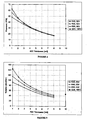
- the pressures and displacements generated by stiffened piezoelectric elements having particular thicknesses and radii of curvature are listed in Table 1. Pressures and total volume generated by stiffened piezoelectric elements are depicted in Figs. 4 and 5 .
- a comparative example of a flat piezoelectric element at a jetting voltage of 100 volts in shear mode is included as a comparison.
- ANSYS multiphysics coupled field analysis was employed using the parameters of an ink chamber diameter of 0.102 cm, lead zirconium titanate (PZT 5A) poled in thickness direction, a cavity plate constructed of KOVAR®, land piezoelectric width (the distance between chambers) of 0.254 mm, an ink density of 1000 kg/m 3 , a pulse voltage of 50 volts, piezoelectric element thickness ranging from 1 mil (25.4 microns) to 10 mils (254 microns) and a radius of curvature of 20 mils, 30 mils, 40 mils, 50 mils or infinity (flat).
- the volume of pumping chamber was kept at 3.14 x 10 -10 m 3 , which is same as the total volume in the comparative case.
- the chamber depth becomes a variable.
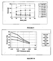
- the pressures and drop volumes generated by stiffened piezoelectric elements having particular thicknesses and radii of curvature are listed in Table 2. Chamber pressures and drop volumes generated by stiffened piezoelectric elements are depicted in Figs. 7 and 8 . A comparative example of a flat piezoelectric element at a jetting voltage of 100 volts in shear mode is included as a comparison.
- ANSYS multiphysics coupled field analysis was employed using the parameters of an ink chamber diameter of 0.102 cm, an ink chamber depth of 0.152 mm, lead zirconium titanate (PZT 5A) poled in thickness direction, a cavity plate constructed of KOVAR®, land piezoelectric width (the distance between chambers) of 0.254 mm, an ink density of 1000 kg/m 3 , a pulse voltage of 50 volts, piezoelectric element thickness ranging from 1 mil (25.4 microns) to 8 mils (203 microns) and a radius of curvature of 20 mils, 30 mils, 40 mils, or 50 mils.
- PZT 5A lead zirconium titanate
- the chamber depth becomes a variable.
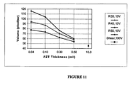
- the drop volumes generated by stiffened piezoelectric elements having particular thicknesses and radii of curvature are depicted in Fig. 9 .
- ANSYS multiphysics coupled field analysis was employed using the parameters of an ink chamber diameter of 0.102 cm, an ink chamber depth of 0.152 mm, lead zirconium titanate (PZT 5A) poled in thickness direction, a cavity plate constructed of KOVAR®, land piezoelectric width (the distance between chambers) of 0.254 mm, an ink density of 1000 kg/m 3 , a pulse voltage of 15 volts, piezoelectric element thickness of 0.04 mil (1 micron), 0.10 mil (2.5 microns), 0.30 mil (7.5 microns), 0.50 mil (12.5 microns) or 10 mils (254 microns) and a radius of curvature of 30 mils, 40 mils, 50 mils or infinity (flat).
- the chamber depth becomes a variable.
- the pressures and drop volumes generated by stiffened piezoelectric elements having particular thicknesses and radii of curvature are listed in Table 3. Chamber pressures and drop volumes generated by stiffened piezoelectric elements are depicted in Figs. 10 and 11 .
- a comparative example of a flat piezoelectric element at a jetting voltage of 100 volts in shear mode is included as a comparison.
Landscapes
- Engineering & Computer Science (AREA)
- Manufacturing & Machinery (AREA)
- Particle Formation And Scattering Control In Inkjet Printers (AREA)
Claims (19)
- Verfahren zum Aufbringen von Tinte, umfassend:Zuführen von Tinte zu einer Tintenkammer (102); undAnlegen einer Ausstoß-Spannung über einer ersten Elektrode (40) undeiner zweiten Elektrode (52) auf einer Fläche eines versteiften piezoelektrischen Elements (34), um Tinte innerhalb der Kammer (102) einem Ausstoß-Druck auszusetzen, wodurch Tinte von einer Ausgangsöffnung (16) der Tintenkammer (102) aufgebracht wird, wobei das versteifte piezoelektrische Element (34) eine gekrümmte Oberfläche über der Tintenkammer (102) aufweist, wobei die gekrümmte Oberfläche einen im Wesentlichen konstanten Krümmungsradius hat und konkav in Bezug zu der Tintenkammer (102) ist,gekennzeichnet dadurch, dass
die gekrümmte Oberfläche eine sphärische Form hat und das versteifte piezoelektrische Element (34) eine Steifheit in zwei Dimensionen hat, die größer ist als ein flaches piezoelektrisches Element. - Verfahren nach Anspruch 1, wobei das piezoelektrische Element (34) Bleizirkoniumtitanat beinhaltet.
- Verfahren nach Anspruch 1, wobei die Ausstoß-Spannung weniger als 60 Volt beträgt.
- Verfahren nach Anspruch 1, wobei die gekrümmte Oberfläche einen Krümmungsradius von weniger als 5 Millimetern hat.
- Tintenstrahldruckmodul, umfassend:eine Tintenkammer (102);ein versteiftes piezoelektrisches Element (34), das eine gekrümmte Oberfläche über der Tintenkammer (102) aufweist, wobei die gekrümmte Oberfläche einen im Wesentlichen konstanten Krümmungsradius hat undkonkav in Bezug auf die Tintenkammer (102) ist, wobei das piezoelektrische Element (34 über der Tintenkammer (102)) positioniert ist, um Tinte innerhalb der Kammer (102) auf einem Ausstoß-Druck auszusetzen; undelektrische Kontakte (40, 52), angeordnet auf einer Oberfläche des piezoelektrischen Elements (34) zur Aktivierung des piezoelektrischen Elements (34),gekennzeichnet dadurch, dass
die gekrümmte Oberfläche eine sphärische Form hat und dass das versteifte piezoelektrische Element (34) eine Steifheit in zwei Dimensionen aufweist, die größer ist als ein flaches piezoelektrisches Element. - Tintenstrahldruckmodul gemäß Anspruch 5, wobei das piezoelektrische Element (34) Bleizirkoniumtitanat beinhaltet.
- Tintenstrahldruckmodul gemäß Anspruch 5, wobei das piezoelektrische Element (34) eine Dicke von 5 bis 300 Mikrometern hat.
- Tintenstrahldruckmodul gemäß Anspruch 5, wobei das piezoelektrische Element (34) eine Dicke von 10 bis 250 Mikrometern hat.
- Tintenstrahldruckmodul gemäß Anspruch 5, wobei das piezoelektrische Element (34) eine Dicke von weniger als 100 Mikrometern hat.
- Tintenstrahldruckmodul gemäß Anspruch 5, wobei die Kammer (102) eine Breite von weniger als 1.200 Mikrometern hat.
- Tintenstrahldruckmodul gemäß Anspruch 5, wobei die Kammer (102) eine Breite von 50 bis 1.000 Mikrometern hat.
- Tintenstrahldruckmodul gemäß Anspruch 5, wobei die Kammer (102) eine Breite von 100 bis 800 Mikrometern hat.
- Tintenstrahldmckinodul gemäß Anspruch 5, wobei die gekrümmte Oberfläche einen Krümmungsradius von 500 bis 3.000 Mikrometern hat.
- Tintenstrahldruckmodul gemäß Anspruch 5, wobei die gekrümmte Oberfläche einen Krümmungsradius von 1.000 bis 2.800 Mikrometern hat.
- Tintenstrahldruckmodul gemäß Anspruch 5, wobei die gekrümmte Oberfläche einen Krümmungsradius von 1.500 bis 2.600 Mikrometern hat.
- Tintenstrahldruckmodul gemäß Anspruch 5, wobei die Elektroden (40, 52) angepasst sind, um eine Spannung von weniger als 60 Volt anzulegen.
- Tintenstrahldruckmodul gemäß Anspruch 5, weiter umfassend eine Reihe von Kammern (102).
- Tintenstrahldruckmodul gemäß Anspruch 17, wobei jede der Kammern (102) durch ein einzelnes piezoelektrisches Element abgedeckt ist.
- Tintenstrahldruckmodul gemäß Anspruch 5, wobei die Kammer (102) eine Wand (104) beinhaltet, die das piezoelektrische Element kontaktiert, das in Kontakt ist mit der Tintenkammer (102) in einem Winkel von mehr als 90 Grad.
Priority Applications (1)
| Application Number | Priority Date | Filing Date | Title |
|---|---|---|---|
| EP10177930A EP2255963B1 (de) | 2001-12-18 | 2002-12-13 | Niederspannungs-tintenstrahlmodul |
Applications Claiming Priority (3)
| Application Number | Priority Date | Filing Date | Title |
|---|---|---|---|
| US20217 | 1979-03-14 | ||
| US10/020,217 US6824253B2 (en) | 2001-12-18 | 2001-12-18 | Low voltage ink jet printing module |
| PCT/US2002/039889 WO2003051635A2 (en) | 2001-12-18 | 2002-12-13 | Low voltage ink jet printing module |
Publications (3)
| Publication Number | Publication Date |
|---|---|
| EP1456034A2 EP1456034A2 (de) | 2004-09-15 |
| EP1456034A4 EP1456034A4 (de) | 2006-03-15 |
| EP1456034B1 true EP1456034B1 (de) | 2010-10-20 |
Family
ID=21797374
Family Applications (2)
| Application Number | Title | Priority Date | Filing Date |
|---|---|---|---|
| EP02799941A Expired - Lifetime EP1456034B1 (de) | 2001-12-18 | 2002-12-13 | Niederspannungs-tintenstrahlmodul |
| EP10177930A Expired - Lifetime EP2255963B1 (de) | 2001-12-18 | 2002-12-13 | Niederspannungs-tintenstrahlmodul |
Family Applications After (1)
| Application Number | Title | Priority Date | Filing Date |
|---|---|---|---|
| EP10177930A Expired - Lifetime EP2255963B1 (de) | 2001-12-18 | 2002-12-13 | Niederspannungs-tintenstrahlmodul |
Country Status (8)
| Country | Link |
|---|---|
| US (1) | US6824253B2 (de) |
| EP (2) | EP1456034B1 (de) |
| JP (1) | JP4287278B2 (de) |
| CN (1) | CN1308145C (de) |
| AT (1) | ATE485165T1 (de) |
| AU (1) | AU2002364563A1 (de) |
| DE (1) | DE60238078D1 (de) |
| WO (1) | WO2003051635A2 (de) |
Families Citing this family (11)
| Publication number | Priority date | Publication date | Assignee | Title |
|---|---|---|---|---|
| US7204586B2 (en) * | 2001-12-18 | 2007-04-17 | Dimatix, Inc. | Ink jet printing module |
| US7267418B2 (en) * | 2003-12-09 | 2007-09-11 | Konica Minolta Business Technologies, Inc. | Ink jet printer |
| US20080061471A1 (en) * | 2006-09-13 | 2008-03-13 | Spin Master Ltd. | Decorative moulding toy |
| US8042913B2 (en) | 2006-09-14 | 2011-10-25 | Hewlett-Packard Development Company, L.P. | Fluid ejection device with deflective flexible membrane |
| US7914125B2 (en) | 2006-09-14 | 2011-03-29 | Hewlett-Packard Development Company, L.P. | Fluid ejection device with deflective flexible membrane |
| US7651204B2 (en) * | 2006-09-14 | 2010-01-26 | Hewlett-Packard Development Company, L.P. | Fluid ejection device |
| JP2013538446A (ja) | 2010-07-26 | 2013-10-10 | 富士フイルム株式会社 | 湾曲圧電膜を有するデバイスの形成 |
| US9070861B2 (en) | 2011-02-15 | 2015-06-30 | Fujifilm Dimatix, Inc. | Piezoelectric transducers using micro-dome arrays |
| JP2013151073A (ja) * | 2012-01-24 | 2013-08-08 | Seiko Epson Corp | 液体噴射装置、および、液体噴射装置の制御方法 |
| CN108705864B (zh) * | 2018-07-26 | 2024-04-05 | 南京沃航智能科技有限公司 | 高效低压驱动压电喷头 |
| CN113043582B (zh) * | 2019-12-26 | 2023-03-31 | 中国科学技术大学 | 一种提高聚合物材料压电响应的方法 |
Family Cites Families (18)
| Publication number | Priority date | Publication date | Assignee | Title |
|---|---|---|---|---|
| US4058809A (en) | 1972-06-26 | 1977-11-15 | Control Data Corporation | MTI system and method |
| US3962063A (en) | 1974-12-18 | 1976-06-08 | Advanced Materials Systems, Inc. | Selective plating apparatus |
| US4588998A (en) * | 1983-07-27 | 1986-05-13 | Ricoh Company, Ltd. | Ink jet head having curved ink |
| US5340510A (en) | 1993-04-05 | 1994-08-23 | Materials Systems Incorporated | Method for making piezoelectric ceramic/polymer composite transducers |
| IT1268870B1 (it) * | 1993-08-23 | 1997-03-13 | Seiko Epson Corp | Testa di registrazione a getto d'inchiostro e procedimento per la sua fabbricazione. |
| JPH07285221A (ja) * | 1994-04-19 | 1995-10-31 | Sharp Corp | インクジェットヘッド |
| JP3501860B2 (ja) * | 1994-12-21 | 2004-03-02 | 日本碍子株式会社 | 圧電/電歪膜型素子及びその製造方法 |
| US5598050A (en) | 1995-02-17 | 1997-01-28 | Materials Systems Inc. | Acoustic actuator and flextensional cover plate there for |
| US5691960A (en) | 1995-08-02 | 1997-11-25 | Materials Systems, Inc. | Conformal composite acoustic transducer panel and method of fabrication thereof |
| US5812163A (en) * | 1996-02-13 | 1998-09-22 | Hewlett-Packard Company | Ink jet printer firing assembly with flexible film expeller |
| EP0803918B2 (de) | 1996-04-11 | 2010-10-20 | Seiko Epson Corporation | Piezolelektrischer Vibrator, diesen piezoelektrischen Vibrator verwendender Tintenstrahldruckkopf und Verfahren zur Herstellung |
| US5841736A (en) | 1997-04-28 | 1998-11-24 | Materials Systems Incorporated | Low voltage piezoelectric transducer and method |
| US6111818A (en) | 1997-04-28 | 2000-08-29 | Materials Systems Inc. | Low voltage piezoelectric actuator |
| US6107726A (en) | 1997-07-25 | 2000-08-22 | Materials Systems, Inc. | Serpentine cross-section piezoelectric linear actuator |
| JP4283948B2 (ja) * | 1998-09-03 | 2009-06-24 | パナソニック株式会社 | インクジェットヘッドの製造方法 |
| US6361154B1 (en) * | 1998-09-03 | 2002-03-26 | Matsushita Electric Industrial Co., Ltd. | Ink-jet head with piezoelectric actuator |
| US6217150B1 (en) | 1999-06-11 | 2001-04-17 | Lexmark International, Inc. | Method of printing with an ink jet printer using multiple carriage speeds |
| US6903491B2 (en) * | 2001-04-26 | 2005-06-07 | Matsushita Electric Industrial Co., Ltd. | Piezoelectric element, actuator, and inkjet head |
-
2001
- 2001-12-18 US US10/020,217 patent/US6824253B2/en not_active Expired - Lifetime
-
2002
- 2002-12-13 AU AU2002364563A patent/AU2002364563A1/en not_active Abandoned
- 2002-12-13 DE DE60238078T patent/DE60238078D1/de not_active Expired - Lifetime
- 2002-12-13 EP EP02799941A patent/EP1456034B1/de not_active Expired - Lifetime
- 2002-12-13 EP EP10177930A patent/EP2255963B1/de not_active Expired - Lifetime
- 2002-12-13 CN CNB028252403A patent/CN1308145C/zh not_active Expired - Lifetime
- 2002-12-13 AT AT02799941T patent/ATE485165T1/de not_active IP Right Cessation
- 2002-12-13 JP JP2003552544A patent/JP4287278B2/ja not_active Expired - Lifetime
- 2002-12-13 WO PCT/US2002/039889 patent/WO2003051635A2/en not_active Ceased
Also Published As
| Publication number | Publication date |
|---|---|
| HK1069359A1 (en) | 2005-05-20 |
| ATE485165T1 (de) | 2010-11-15 |
| DE60238078D1 (de) | 2010-12-02 |
| EP2255963A8 (de) | 2011-06-01 |
| AU2002364563A8 (en) | 2003-06-30 |
| EP1456034A2 (de) | 2004-09-15 |
| EP2255963A1 (de) | 2010-12-01 |
| CN1604850A (zh) | 2005-04-06 |
| EP2255963B1 (de) | 2012-10-31 |
| US20030112319A1 (en) | 2003-06-19 |
| US6824253B2 (en) | 2004-11-30 |
| HK1149732A1 (en) | 2011-10-14 |
| JP2005512844A (ja) | 2005-05-12 |
| EP1456034A4 (de) | 2006-03-15 |
| CN1308145C (zh) | 2007-04-04 |
| WO2003051635A3 (en) | 2003-12-18 |
| WO2003051635A2 (en) | 2003-06-26 |
| AU2002364563A1 (en) | 2003-06-30 |
| JP4287278B2 (ja) | 2009-07-01 |
Similar Documents
| Publication | Publication Date | Title |
|---|---|---|
| JP3329125B2 (ja) | インクジェット記録装置 | |
| EP0732209B1 (de) | Verfahren zur Herstellung eines piezoelektrischen Schichtelementes | |
| JP3106026B2 (ja) | 圧電/電歪アクチュエータ | |
| US5912526A (en) | Layered-type piezoelectric element and method for producing the layered-type piezoelectric element | |
| JP2012096554A (ja) | インクジェット・プリンティングモジュール | |
| JPH04341853A (ja) | 圧電式インクジェットプリンタヘッド | |
| EP1456034B1 (de) | Niederspannungs-tintenstrahlmodul | |
| US7891782B2 (en) | Liquid injecting head, method of manufacturing liquid injecting head, and liquid injecting device | |
| EP1652670B1 (de) | Vorrichtung zum Transport von Flüssigkeiten | |
| HK1069359B (en) | Low voltage ink jet printing module | |
| HK1149732B (en) | Low voltage ink jet printing module | |
| CN1486792A (zh) | 液体喷头 | |
| JP2842394B2 (ja) | 圧電素子の製造方法 | |
| JP3485014B2 (ja) | インクジェット式記録ヘッド及びインクジェット式記録装置 | |
| JPH03264360A (ja) | インクジェット記録ヘッド | |
| JPH0550606A (ja) | インクジエツトプリンタヘツド用圧電素子の製造方法 | |
| JPH05309841A (ja) | インクジェットプリンタヘッドの製作方法 | |
| JP2729008B2 (ja) | インクジェット記録ヘッド装置 | |
| HK1151772A (en) | Ink jet printing module | |
| JPH05254133A (ja) | インクジェットプリンタヘッドの製作方法 | |
| JPH11138802A (ja) | インクジェット式記録ヘッド | |
| JPH03162963A (ja) | インクジェットヘッド | |
| JPH07214772A (ja) | 圧電駆動形インクジェットヘッド |
Legal Events
| Date | Code | Title | Description |
|---|---|---|---|
| PUAI | Public reference made under article 153(3) epc to a published international application that has entered the european phase |
Free format text: ORIGINAL CODE: 0009012 |
|
| 17P | Request for examination filed |
Effective date: 20040614 |
|
| AK | Designated contracting states |
Kind code of ref document: A2 Designated state(s): AT BE BG CH CY CZ DE DK EE ES FI FR GB GR IE IT LI LU MC NL PT SE SI SK TR |
|
| AX | Request for extension of the european patent |
Extension state: AL LT LV MK RO |
|
| REG | Reference to a national code |
Ref country code: HK Ref legal event code: DE Ref document number: 1069359 Country of ref document: HK |
|
| RAP1 | Party data changed (applicant data changed or rights of an application transferred) |
Owner name: DIMATIX, INC. |
|
| A4 | Supplementary search report drawn up and despatched |
Effective date: 20060126 |
|
| 17Q | First examination report despatched |
Effective date: 20080220 |
|
| RAP1 | Party data changed (applicant data changed or rights of an application transferred) |
Owner name: FUJIFILM DIMATIX, INC. |
|
| GRAP | Despatch of communication of intention to grant a patent |
Free format text: ORIGINAL CODE: EPIDOSNIGR1 |
|
| GRAS | Grant fee paid |
Free format text: ORIGINAL CODE: EPIDOSNIGR3 |
|
| GRAA | (expected) grant |
Free format text: ORIGINAL CODE: 0009210 |
|
| AK | Designated contracting states |
Kind code of ref document: B1 Designated state(s): AT BE BG CH CY CZ DE DK EE ES FI FR GB GR IE IT LI LU MC NL PT SE SI SK TR |
|
| REG | Reference to a national code |
Ref country code: GB Ref legal event code: FG4D |
|
| REG | Reference to a national code |
Ref country code: CH Ref legal event code: EP |
|
| REG | Reference to a national code |
Ref country code: IE Ref legal event code: FG4D |
|
| REF | Corresponds to: |
Ref document number: 60238078 Country of ref document: DE Date of ref document: 20101202 Kind code of ref document: P |
|
| REG | Reference to a national code |
Ref country code: NL Ref legal event code: VDEP Effective date: 20101020 |
|
| REG | Reference to a national code |
Ref country code: HK Ref legal event code: GR Ref document number: 1069359 Country of ref document: HK |
|
| PG25 | Lapsed in a contracting state [announced via postgrant information from national office to epo] |
Ref country code: SE Free format text: LAPSE BECAUSE OF FAILURE TO SUBMIT A TRANSLATION OF THE DESCRIPTION OR TO PAY THE FEE WITHIN THE PRESCRIBED TIME-LIMIT Effective date: 20101020 Ref country code: FI Free format text: LAPSE BECAUSE OF FAILURE TO SUBMIT A TRANSLATION OF THE DESCRIPTION OR TO PAY THE FEE WITHIN THE PRESCRIBED TIME-LIMIT Effective date: 20101020 Ref country code: NL Free format text: LAPSE BECAUSE OF FAILURE TO SUBMIT A TRANSLATION OF THE DESCRIPTION OR TO PAY THE FEE WITHIN THE PRESCRIBED TIME-LIMIT Effective date: 20101020 Ref country code: PT Free format text: LAPSE BECAUSE OF FAILURE TO SUBMIT A TRANSLATION OF THE DESCRIPTION OR TO PAY THE FEE WITHIN THE PRESCRIBED TIME-LIMIT Effective date: 20110221 Ref country code: BG Free format text: LAPSE BECAUSE OF FAILURE TO SUBMIT A TRANSLATION OF THE DESCRIPTION OR TO PAY THE FEE WITHIN THE PRESCRIBED TIME-LIMIT Effective date: 20110120 Ref country code: AT Free format text: LAPSE BECAUSE OF FAILURE TO SUBMIT A TRANSLATION OF THE DESCRIPTION OR TO PAY THE FEE WITHIN THE PRESCRIBED TIME-LIMIT Effective date: 20101020 Ref country code: SI Free format text: LAPSE BECAUSE OF FAILURE TO SUBMIT A TRANSLATION OF THE DESCRIPTION OR TO PAY THE FEE WITHIN THE PRESCRIBED TIME-LIMIT Effective date: 20101020 |
|
| PG25 | Lapsed in a contracting state [announced via postgrant information from national office to epo] |
Ref country code: GR Free format text: LAPSE BECAUSE OF FAILURE TO SUBMIT A TRANSLATION OF THE DESCRIPTION OR TO PAY THE FEE WITHIN THE PRESCRIBED TIME-LIMIT Effective date: 20110121 Ref country code: BE Free format text: LAPSE BECAUSE OF FAILURE TO SUBMIT A TRANSLATION OF THE DESCRIPTION OR TO PAY THE FEE WITHIN THE PRESCRIBED TIME-LIMIT Effective date: 20101020 |
|
| PG25 | Lapsed in a contracting state [announced via postgrant information from national office to epo] |
Ref country code: MC Free format text: LAPSE BECAUSE OF NON-PAYMENT OF DUE FEES Effective date: 20101231 Ref country code: CZ Free format text: LAPSE BECAUSE OF FAILURE TO SUBMIT A TRANSLATION OF THE DESCRIPTION OR TO PAY THE FEE WITHIN THE PRESCRIBED TIME-LIMIT Effective date: 20101020 Ref country code: ES Free format text: LAPSE BECAUSE OF FAILURE TO SUBMIT A TRANSLATION OF THE DESCRIPTION OR TO PAY THE FEE WITHIN THE PRESCRIBED TIME-LIMIT Effective date: 20110131 Ref country code: EE Free format text: LAPSE BECAUSE OF FAILURE TO SUBMIT A TRANSLATION OF THE DESCRIPTION OR TO PAY THE FEE WITHIN THE PRESCRIBED TIME-LIMIT Effective date: 20101020 |
|
| REG | Reference to a national code |
Ref country code: CH Ref legal event code: PL |
|
| PLBE | No opposition filed within time limit |
Free format text: ORIGINAL CODE: 0009261 |
|
| STAA | Information on the status of an ep patent application or granted ep patent |
Free format text: STATUS: NO OPPOSITION FILED WITHIN TIME LIMIT |
|
| PG25 | Lapsed in a contracting state [announced via postgrant information from national office to epo] |
Ref country code: DK Free format text: LAPSE BECAUSE OF FAILURE TO SUBMIT A TRANSLATION OF THE DESCRIPTION OR TO PAY THE FEE WITHIN THE PRESCRIBED TIME-LIMIT Effective date: 20101020 Ref country code: SK Free format text: LAPSE BECAUSE OF FAILURE TO SUBMIT A TRANSLATION OF THE DESCRIPTION OR TO PAY THE FEE WITHIN THE PRESCRIBED TIME-LIMIT Effective date: 20101020 |
|
| 26N | No opposition filed |
Effective date: 20110721 |
|
| PG25 | Lapsed in a contracting state [announced via postgrant information from national office to epo] |
Ref country code: IE Free format text: LAPSE BECAUSE OF NON-PAYMENT OF DUE FEES Effective date: 20101213 Ref country code: LI Free format text: LAPSE BECAUSE OF NON-PAYMENT OF DUE FEES Effective date: 20101231 Ref country code: CH Free format text: LAPSE BECAUSE OF NON-PAYMENT OF DUE FEES Effective date: 20101231 |
|
| REG | Reference to a national code |
Ref country code: DE Ref legal event code: R097 Ref document number: 60238078 Country of ref document: DE Effective date: 20110721 |
|
| PG25 | Lapsed in a contracting state [announced via postgrant information from national office to epo] |
Ref country code: IT Free format text: LAPSE BECAUSE OF FAILURE TO SUBMIT A TRANSLATION OF THE DESCRIPTION OR TO PAY THE FEE WITHIN THE PRESCRIBED TIME-LIMIT Effective date: 20101020 |
|
| PG25 | Lapsed in a contracting state [announced via postgrant information from national office to epo] |
Ref country code: CY Free format text: LAPSE BECAUSE OF FAILURE TO SUBMIT A TRANSLATION OF THE DESCRIPTION OR TO PAY THE FEE WITHIN THE PRESCRIBED TIME-LIMIT Effective date: 20101020 |
|
| PG25 | Lapsed in a contracting state [announced via postgrant information from national office to epo] |
Ref country code: LU Free format text: LAPSE BECAUSE OF NON-PAYMENT OF DUE FEES Effective date: 20101213 |
|
| PG25 | Lapsed in a contracting state [announced via postgrant information from national office to epo] |
Ref country code: TR Free format text: LAPSE BECAUSE OF FAILURE TO SUBMIT A TRANSLATION OF THE DESCRIPTION OR TO PAY THE FEE WITHIN THE PRESCRIBED TIME-LIMIT Effective date: 20101020 |
|
| REG | Reference to a national code |
Ref country code: FR Ref legal event code: PLFP Year of fee payment: 14 |
|
| REG | Reference to a national code |
Ref country code: FR Ref legal event code: PLFP Year of fee payment: 15 |
|
| REG | Reference to a national code |
Ref country code: FR Ref legal event code: PLFP Year of fee payment: 16 |
|
| PGFP | Annual fee paid to national office [announced via postgrant information from national office to epo] |
Ref country code: FR Payment date: 20211109 Year of fee payment: 20 Ref country code: GB Payment date: 20211028 Year of fee payment: 20 Ref country code: DE Payment date: 20211102 Year of fee payment: 20 |
|
| REG | Reference to a national code |
Ref country code: DE Ref legal event code: R071 Ref document number: 60238078 Country of ref document: DE |
|
| REG | Reference to a national code |
Ref country code: GB Ref legal event code: PE20 Expiry date: 20221212 |
|
| PG25 | Lapsed in a contracting state [announced via postgrant information from national office to epo] |
Ref country code: GB Free format text: LAPSE BECAUSE OF EXPIRATION OF PROTECTION Effective date: 20221212 |