EP1458025A2 - Circuits intégrés à lignes d'alimentation électrique séparées - Google Patents
Circuits intégrés à lignes d'alimentation électrique séparées Download PDFInfo
- Publication number
- EP1458025A2 EP1458025A2 EP03027229A EP03027229A EP1458025A2 EP 1458025 A2 EP1458025 A2 EP 1458025A2 EP 03027229 A EP03027229 A EP 03027229A EP 03027229 A EP03027229 A EP 03027229A EP 1458025 A2 EP1458025 A2 EP 1458025A2
- Authority
- EP
- European Patent Office
- Prior art keywords
- integrated circuit
- circuit according
- doping
- conductivity type
- zone
- Prior art date
- Legal status (The legal status is an assumption and is not a legal conclusion. Google has not performed a legal analysis and makes no representation as to the accuracy of the status listed.)
- Granted
Links
Images



Classifications
-
- H—ELECTRICITY
- H10—SEMICONDUCTOR DEVICES; ELECTRIC SOLID-STATE DEVICES NOT OTHERWISE PROVIDED FOR
- H10D—INORGANIC ELECTRIC SEMICONDUCTOR DEVICES
- H10D89/00—Aspects of integrated devices not covered by groups H10D84/00 - H10D88/00
- H10D89/60—Integrated devices comprising arrangements for electrical or thermal protection, e.g. protection circuits against electrostatic discharge [ESD]
- H10D89/601—Integrated devices comprising arrangements for electrical or thermal protection, e.g. protection circuits against electrostatic discharge [ESD] for devices having insulated gate electrodes, e.g. for IGFETs or IGBTs
- H10D89/711—Integrated devices comprising arrangements for electrical or thermal protection, e.g. protection circuits against electrostatic discharge [ESD] for devices having insulated gate electrodes, e.g. for IGFETs or IGBTs using bipolar transistors as protective elements
-
- H—ELECTRICITY
- H10—SEMICONDUCTOR DEVICES; ELECTRIC SOLID-STATE DEVICES NOT OTHERWISE PROVIDED FOR
- H10W—GENERIC PACKAGES, INTERCONNECTIONS, CONNECTORS OR OTHER CONSTRUCTIONAL DETAILS OF DEVICES COVERED BY CLASS H10
- H10W42/00—Arrangements for protection of devices
- H10W42/80—Arrangements for protection of devices protecting against overcurrent or overload, e.g. fuses or shunts
Definitions
- the present invention relates to an integrated circuit with at least two circuit parts on a common Semiconductor substrate are formed and each have their own Supply voltage networks each have their own bond spots for feeding in a supply voltage supplied from outside exhibit.
- Such separate supply voltage networks can e.g. may be necessary for EMC reasons. at is the usual technology for highly integrated circuits the semiconductor substrate is p-conducting and with the supply node two circuit parts that have the lowest potential "Vss" below the applied potentials, connected by substrate contacts, so the Vss potentials of the two circuit parts are coupled by a substrate resistor.
- Coupling circuits 3, 4 between the supply potentials Vcc1 and Vcc2 or Vss1 and Vss2 are each due to anti-parallel circuits of two pnp transistors 6 formed. If there is an overvoltage the supply voltage networks the circuit parts 1, 2 against each other warps, voltage compensation takes place via the transistors 6, part of the current from the emitter to the base and the rest continues to flow to the collector.
- the pnp transistors 6 each have the semiconductor substrate as a collector, an n-doped well formed in the substrate as the base and a p + region within the well as the emitter.
- Such a construction has the effect that if one of the coupling circuits 3 or 4 opens in the event of an overvoltage, part of the equalizing current (from the emitter to the base) will flow from one supply network to the other, but inevitably part will also flow directly from the emitter into the substrate that represents the collector.
- the object of the invention is an integrated circuit with at least two circuit parts and separate supply voltage networks to indicate for the different circuit parts, which is a simply structured coupling circuit with little Has area requirement between the supply voltage networks.
- the basis of the Transistor through the substrate itself, more precisely through one at collector and emitter doping zones of the transistor adjacent region of the substrate is formed, and the resistance between the base and those coupled by the coupling circuit
- the potential of the two networks is the intrinsic resistance of the substrate between its base region and one contact doping zone each with the collector or the emitter by a metallization applied to the substrate is conductively connected.
- the coupling circuit according to the invention with a single transistor can be realized, its dimensions are determined by the desired volume resistance. Greater freedom in terms of accommodation the coupling circuit on a substrate surface without increased space requirement results in use several transistors. In principle, these can be independent be distributed from one another on the substrate surface.
- a particularly space-saving design results if the transistors through a plurality of doping zones of the second conductivity type are formed, which alternate with connected to one and the other of the two supply potentials are. If one with the supply potential of the first circuit part connected doping zone at two Pages - each with an intermediate, the natural Doping of the substrate-containing base zone - from with the Supply potential of the second circuit part connected Such an arrangement corresponds to doping zones two parallel transistors.
- the surface requirement for two transistors is therefore clear in such an arrangement less than twice the space requirement of two individual transistors, and the space saving can be increased, if more than two transistors by a corresponding one alternating arrangement of with the two supply potentials connected doping zones are formed.
- the contact doping zones are preferably at the ends of the Row arranged. Two contact doping zones are therefore sufficient for a plurality of transistors, which in turn is a Space saving results.
- the number of doping zones forming the emitters of the second conductivity type is 4, which is a parallel connection of three transistors.
- the at least one transistor the coupling circuit from a shielding doping zone of the second Conductivity type is surrounded.
- a shielding doping zone is advantageously biased in the reverse direction, so that there is a barrier layer between it and the substrate formed.
- the shielding doping zone is preferably ring-shaped along the surface of the substrate. It therefore prevents not any current flow from the at least one transistor the coupling circuit through the substrate to the circuit parts, it forces the load carriers to take a detour the depth of the substrate, which changes their path and thus the effective resistance of the substrate between the transistors the coupling circuit and the circuit parts increased.
- the contact doping zones of the coupling circuit are preferred surrounded by the shielding doping zone.
- the coupling circuit shown in Fig. 2 is provided to the conventional coupling circuit 4 of the integrated circuit Fig. 1 to replace.
- An NPN transistor 11 whose geometry and doping are completely symmetrical and therefore with two emitters is shown, is over the one emitter with Vss1 and connected to Vss2 via the other.
- the two supply potentials Vss1, Vss2 are each via identical resistors 12 connected to the base of transistor 11.
- Fig. 3 shows the current-voltage characteristic of the coupling circuit from Fig. 2. With small differences between the two supply potentials the behavior is purely resistive and through that Resistors 12 determined; with increasing tensions the Activity of the transistor 11, and through the coupling circuit flowing equalizing current I takes more than linear with the voltage V too.
- Fig. 4 shows a first example of a practical layout of a switching circuit according to the invention.
- a p - -doped semiconductor substrate On a p - -doped semiconductor substrate, six doping zones 14 to 19 are formed in a row next to one another, of which the two outermost p + -doped and are referred to as contact doping zones 14, 19 and the so-called emitter doping zones 15 to 18 n + in between . are endowed.
- Surface metallizations of the doping zones 14, 16, 18 are connected to Vss1, those of the doping zones 15, 17, 19 to Vss2.
- Surface strips 20, 21, 22 of the substrate 13 lying between the emitter doping zones 15 to 18 have its original p - doping in a doping concentration not changed by the generation of the doping zones 14 to 19.
- These surface strips 20, 21 or 22 each function as the base of a symmetrical transistor, the two emitters of which. two emitter doping zones adjacent to the relevant surface strips 20 are formed.
- the contact doping zones 14, 19 allow a current to flow through the substrate 13 from one contact doping zone 14, 19 to the other. This current flow determines the electrical potentials effective in the area of the individual surface strips 20, 21, 22.
- the equivalent circuit diagram shown in FIG. 5 therefore corresponds to the layout of FIG. 4. It can be clearly seen here that the two middle emitter doping zones 16, 17 of the layout from FIG.
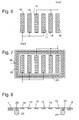
- FIG. 6 shows a second embodiment of a layout of a Coupling circuit. It differs from that shown in FIG. 4 Layout in that the associated with Vss1 or Vss2 Emitter zones are interchanged so that the neighboring ones Doping zones 14 and 15 or 18 and 19 each over a metallization are connected in parallel. Because this way the distance between the contact implantation zones 14 or 19 and the next neighboring one, with the respective other supply voltage connected emitter doping zones 16, 17 opposite 4 is enlarged and accordingly the substrate resistance is also increased accordingly the danger that a surge pulse will breakdown a pn boundary layer of the emitter doping zones, reduced.
- the dielectric strength is the same Dimensioning and arrangement of the doping zones opposite 4 improved, or the width of the Surface stripes between the contact doping zones 14, 19 and the emitter doping zones 15 and 18 adjacent to them can be reduced while maintaining the same dielectric strength, whereby the space requirement of the coupling circuit continues reduced.
- FIG. 7 shows a further development of the layout from Fig. 6. Since the by the surface strips 20 to 22 and the emitter doping zones 15 to 18 formed adjacent to them Transistors inevitably coupled to the substrate 13 are used to reduce interactions between the transistors of the coupling circuit and the elements of the Circuit parts 1, 2 a shielding doping zone 23 is provided, by n-doping with a high penetration depth into the substrate 13 is formed.
- the shielding doping zone 23 is on the surface of the substrate 13 on a small cross-sectional area heavily n-doped to form a contact zone 25, those in conductive contact with one on the substrate surface deposited metallization 24.
- Fig. 9 also shows a further developed embodiment of the layout from FIG. 6.
- the shielding doping zone 23 surrounds the emitter doping zones 15 to 18 in a ring.
- 7 is not the contact zone 25 arranged in a ring around the transistors of the coupling circuit, but it is limited to two islands with each one of the two potentials Vss1, Vss2 conductively connected are.
- the doping concentration in the shielding doping zone 23 can be kept low, their conductivity can kept at a similar low value as that of the substrate 13 become.
Landscapes
- Semiconductor Integrated Circuits (AREA)
- Bipolar Integrated Circuits (AREA)
- Emergency Protection Circuit Devices (AREA)
Applications Claiming Priority (2)
| Application Number | Priority Date | Filing Date | Title |
|---|---|---|---|
| DE10301586A DE10301586B3 (de) | 2003-01-17 | 2003-01-17 | Integrierte Schaltung |
| DE10301586 | 2003-01-17 |
Publications (3)
| Publication Number | Publication Date |
|---|---|
| EP1458025A2 true EP1458025A2 (fr) | 2004-09-15 |
| EP1458025A3 EP1458025A3 (fr) | 2007-04-18 |
| EP1458025B1 EP1458025B1 (fr) | 2009-06-03 |
Family
ID=30775635
Family Applications (1)
| Application Number | Title | Priority Date | Filing Date |
|---|---|---|---|
| EP03027229A Expired - Lifetime EP1458025B1 (fr) | 2003-01-17 | 2003-11-28 | Circuits intégrés à lignes d'alimentation électrique séparées |
Country Status (6)
| Country | Link |
|---|---|
| US (1) | US7202532B2 (fr) |
| EP (1) | EP1458025B1 (fr) |
| JP (1) | JP4555578B2 (fr) |
| KR (1) | KR101190427B1 (fr) |
| AT (1) | ATE433198T1 (fr) |
| DE (2) | DE10301586B3 (fr) |
Families Citing this family (2)
| Publication number | Priority date | Publication date | Assignee | Title |
|---|---|---|---|---|
| US7321501B2 (en) * | 2005-06-09 | 2008-01-22 | United Microelectronics Corp. | Method for trimming programmable resistor to predetermined resistance |
| US7626243B2 (en) * | 2006-08-04 | 2009-12-01 | Advanced Analogic Technologies, Inc. | ESD protection for bipolar-CMOS-DMOS integrated circuit devices |
Family Cites Families (7)
| Publication number | Priority date | Publication date | Assignee | Title |
|---|---|---|---|---|
| KR100237992B1 (ko) * | 1995-09-06 | 2000-01-15 | 포만 제프리 엘 | 전원 순서 독립 정전 방전 보호 회로 |
| EP0810503B1 (fr) * | 1996-05-14 | 2001-12-19 | Co.Ri.M.Me. Consorzio Per La Ricerca Sulla Microelettronica Nel Mezzogiorno | Un circuit intégré avec un dispositif ayant un seuil de conduction inverse prédéterminé et un dispositif de compensation thermique avec multiplicateurs de Vbe |
| JPH10290519A (ja) * | 1997-04-15 | 1998-10-27 | Hitachi Ltd | 半導体集積回路装置 |
| US6011681A (en) * | 1998-08-26 | 2000-01-04 | Taiwan Semiconductor Manufacturing Company, Ltd. | Whole-chip ESD protection for CMOS ICs using bi-directional SCRs |
| US6271999B1 (en) * | 1998-11-20 | 2001-08-07 | Taiwan Semiconductor Manufacturing Company | ESD protection circuit for different power supplies |
| WO2002037566A2 (fr) * | 2000-11-06 | 2002-05-10 | Sarnoff Corporation | Dispositif de protection contre des decharges electrostatiques a redresseur au silicium avec declencheur sur puce externe et dimensions internes reduites pour declenchement rapide |
| US6744107B1 (en) * | 2002-12-23 | 2004-06-01 | Silicon Integrated Systems Corp. | ESD protection circuit with self-triggered technique |
-
2003
- 2003-01-17 DE DE10301586A patent/DE10301586B3/de not_active Expired - Fee Related
- 2003-11-28 DE DE50311575T patent/DE50311575D1/de not_active Expired - Lifetime
- 2003-11-28 AT AT03027229T patent/ATE433198T1/de not_active IP Right Cessation
- 2003-11-28 EP EP03027229A patent/EP1458025B1/fr not_active Expired - Lifetime
- 2003-12-30 KR KR1020030099542A patent/KR101190427B1/ko not_active Expired - Fee Related
-
2004
- 2004-01-07 JP JP2004001877A patent/JP4555578B2/ja not_active Expired - Fee Related
- 2004-01-20 US US10/761,144 patent/US7202532B2/en not_active Expired - Fee Related
Also Published As
| Publication number | Publication date |
|---|---|
| KR20040067827A (ko) | 2004-07-30 |
| DE10301586B3 (de) | 2004-02-26 |
| US7202532B2 (en) | 2007-04-10 |
| JP2004228567A (ja) | 2004-08-12 |
| DE50311575D1 (de) | 2009-07-16 |
| KR101190427B1 (ko) | 2012-10-11 |
| US20040178506A1 (en) | 2004-09-16 |
| EP1458025A3 (fr) | 2007-04-18 |
| ATE433198T1 (de) | 2009-06-15 |
| JP4555578B2 (ja) | 2010-10-06 |
| EP1458025B1 (fr) | 2009-06-03 |
Similar Documents
| Publication | Publication Date | Title |
|---|---|---|
| DE69515560T2 (de) | Vorrichtung und Verfahren zum Schutz einer integrierten Schaltung | |
| DE69327357T2 (de) | Integrierte Halbleiterschaltungsanordnung | |
| DE69526630T2 (de) | Verbesserungen in oder in Beziehung auf integrierte Schaltungen | |
| DE102011054700B4 (de) | Halbleiter-ESD-Bauelement und Verfahren | |
| DE102004062214B4 (de) | Halbleitervorrichtung mit Temperaturerfassungsfunktion | |
| DE3834841C2 (de) | Integrierte Anordnung in einem Substrat zur Vermeidung parasitärer Substrateffekte | |
| DE102020125553B4 (de) | Halbleitervorrichtung und verfahren zur herstellung von selbiger | |
| DE69527146T2 (de) | Integriertes MOS-Bauelement mit einer Gateschutzdiode | |
| DE69308051T2 (de) | Schutzdiodennetz bildende integrierte Schaltung | |
| DE102009049051A1 (de) | Halbleitervorrichtung mit IGBT und FWD auf demselben Substrat | |
| DE19654163B4 (de) | Schutzvorrichtung für eine Halbleiterschaltung | |
| EP1703560A2 (fr) | Dispositif de protection contre les décharges electrostatiques (ESD) à current de charge et rigidité diélectrique adjustable | |
| DE69121860T2 (de) | Überspannungen zwischen ausgewählten Grenzen begrenzende Schutzschaltung und deren monolitsche Integration | |
| DE3486077T2 (de) | Integrierte halbleiterschaltungsanordnung. | |
| DE112004002717T5 (de) | Pufferschaltung mit elektrostatischem Entladeschutz | |
| DE102010005715A1 (de) | Transistoranordnung als ESD-Schutzmaßnahme | |
| DE4022022C2 (de) | Vertikal-Halbleitervorrichtung mit Zenerdiode als Überspannugsschutz | |
| DE68916192T2 (de) | Ausgangspuffer einer integrierten Schaltung mit einem verbesserten ESD-Schutz. | |
| DE69033960T2 (de) | Halbleiterbauelement mit MIS-Kondensator | |
| EP1284019B1 (fr) | Composant semi-conducteur de puissance | |
| DE10247431A1 (de) | Halbleitervorrichtung | |
| EP1458025B1 (fr) | Circuits intégrés à lignes d'alimentation électrique séparées | |
| EP1127377B1 (fr) | Transistor de securite a dissipation electrostatique | |
| DE102013113740A1 (de) | ESD-Schutzstruktur, integrierte Schaltung und Halbleiterbauelement | |
| DE2753882C2 (de) | Digitale integrierte Schaltung |
Legal Events
| Date | Code | Title | Description |
|---|---|---|---|
| PUAI | Public reference made under article 153(3) epc to a published international application that has entered the european phase |
Free format text: ORIGINAL CODE: 0009012 |
|
| AK | Designated contracting states |
Kind code of ref document: A2 Designated state(s): AT BE BG CH CY CZ DE DK EE ES FI FR GB GR HU IE IT LI LU MC NL PT RO SE SI SK TR |
|
| AX | Request for extension of the european patent |
Extension state: AL LT LV MK |
|
| PUAL | Search report despatched |
Free format text: ORIGINAL CODE: 0009013 |
|
| AK | Designated contracting states |
Kind code of ref document: A3 Designated state(s): AT BE BG CH CY CZ DE DK EE ES FI FR GB GR HU IE IT LI LU MC NL PT RO SE SI SK TR |
|
| AX | Request for extension of the european patent |
Extension state: AL LT LV MK |
|
| 17P | Request for examination filed |
Effective date: 20070619 |
|
| AKX | Designation fees paid |
Designated state(s): AT BE BG CH CY CZ DE DK EE ES FI FR GB GR HU IE IT LI LU MC NL PT RO SE SI SK TR |
|
| GRAP | Despatch of communication of intention to grant a patent |
Free format text: ORIGINAL CODE: EPIDOSNIGR1 |
|
| GRAS | Grant fee paid |
Free format text: ORIGINAL CODE: EPIDOSNIGR3 |
|
| GRAA | (expected) grant |
Free format text: ORIGINAL CODE: 0009210 |
|
| AK | Designated contracting states |
Kind code of ref document: B1 Designated state(s): AT BE BG CH CY CZ DE DK EE ES FI FR GB GR HU IE IT LI LU MC NL PT RO SE SI SK TR |
|
| REG | Reference to a national code |
Ref country code: GB Ref legal event code: FG4D Free format text: NOT ENGLISH |
|
| REG | Reference to a national code |
Ref country code: CH Ref legal event code: EP |
|
| REG | Reference to a national code |
Ref country code: IE Ref legal event code: FG4D Free format text: LANGUAGE OF EP DOCUMENT: GERMAN |
|
| REF | Corresponds to: |
Ref document number: 50311575 Country of ref document: DE Date of ref document: 20090716 Kind code of ref document: P |
|
| PG25 | Lapsed in a contracting state [announced via postgrant information from national office to epo] |
Ref country code: FI Free format text: LAPSE BECAUSE OF FAILURE TO SUBMIT A TRANSLATION OF THE DESCRIPTION OR TO PAY THE FEE WITHIN THE PRESCRIBED TIME-LIMIT Effective date: 20090603 |
|
| NLV1 | Nl: lapsed or annulled due to failure to fulfill the requirements of art. 29p and 29m of the patents act | ||
| PG25 | Lapsed in a contracting state [announced via postgrant information from national office to epo] |
Ref country code: SE Free format text: LAPSE BECAUSE OF FAILURE TO SUBMIT A TRANSLATION OF THE DESCRIPTION OR TO PAY THE FEE WITHIN THE PRESCRIBED TIME-LIMIT Effective date: 20090903 Ref country code: NL Free format text: LAPSE BECAUSE OF FAILURE TO SUBMIT A TRANSLATION OF THE DESCRIPTION OR TO PAY THE FEE WITHIN THE PRESCRIBED TIME-LIMIT Effective date: 20090603 Ref country code: SI Free format text: LAPSE BECAUSE OF FAILURE TO SUBMIT A TRANSLATION OF THE DESCRIPTION OR TO PAY THE FEE WITHIN THE PRESCRIBED TIME-LIMIT Effective date: 20090603 |
|
| REG | Reference to a national code |
Ref country code: IE Ref legal event code: FD4D |
|
| PG25 | Lapsed in a contracting state [announced via postgrant information from national office to epo] |
Ref country code: ES Free format text: LAPSE BECAUSE OF FAILURE TO SUBMIT A TRANSLATION OF THE DESCRIPTION OR TO PAY THE FEE WITHIN THE PRESCRIBED TIME-LIMIT Effective date: 20090914 Ref country code: EE Free format text: LAPSE BECAUSE OF FAILURE TO SUBMIT A TRANSLATION OF THE DESCRIPTION OR TO PAY THE FEE WITHIN THE PRESCRIBED TIME-LIMIT Effective date: 20090603 Ref country code: CZ Free format text: LAPSE BECAUSE OF FAILURE TO SUBMIT A TRANSLATION OF THE DESCRIPTION OR TO PAY THE FEE WITHIN THE PRESCRIBED TIME-LIMIT Effective date: 20090603 Ref country code: IE Free format text: LAPSE BECAUSE OF FAILURE TO SUBMIT A TRANSLATION OF THE DESCRIPTION OR TO PAY THE FEE WITHIN THE PRESCRIBED TIME-LIMIT Effective date: 20090603 Ref country code: RO Free format text: LAPSE BECAUSE OF FAILURE TO SUBMIT A TRANSLATION OF THE DESCRIPTION OR TO PAY THE FEE WITHIN THE PRESCRIBED TIME-LIMIT Effective date: 20090603 |
|
| PG25 | Lapsed in a contracting state [announced via postgrant information from national office to epo] |
Ref country code: SK Free format text: LAPSE BECAUSE OF FAILURE TO SUBMIT A TRANSLATION OF THE DESCRIPTION OR TO PAY THE FEE WITHIN THE PRESCRIBED TIME-LIMIT Effective date: 20090603 |
|
| PG25 | Lapsed in a contracting state [announced via postgrant information from national office to epo] |
Ref country code: BG Free format text: LAPSE BECAUSE OF FAILURE TO SUBMIT A TRANSLATION OF THE DESCRIPTION OR TO PAY THE FEE WITHIN THE PRESCRIBED TIME-LIMIT Effective date: 20090903 Ref country code: PT Free format text: LAPSE BECAUSE OF FAILURE TO SUBMIT A TRANSLATION OF THE DESCRIPTION OR TO PAY THE FEE WITHIN THE PRESCRIBED TIME-LIMIT Effective date: 20091003 |
|
| PLBE | No opposition filed within time limit |
Free format text: ORIGINAL CODE: 0009261 |
|
| STAA | Information on the status of an ep patent application or granted ep patent |
Free format text: STATUS: NO OPPOSITION FILED WITHIN TIME LIMIT |
|
| PG25 | Lapsed in a contracting state [announced via postgrant information from national office to epo] |
Ref country code: DK Free format text: LAPSE BECAUSE OF FAILURE TO SUBMIT A TRANSLATION OF THE DESCRIPTION OR TO PAY THE FEE WITHIN THE PRESCRIBED TIME-LIMIT Effective date: 20090603 |
|
| 26N | No opposition filed |
Effective date: 20100304 |
|
| BERE | Be: lapsed |
Owner name: MICRONAS G.M.B.H. Effective date: 20091130 |
|
| PG25 | Lapsed in a contracting state [announced via postgrant information from national office to epo] |
Ref country code: MC Free format text: LAPSE BECAUSE OF NON-PAYMENT OF DUE FEES Effective date: 20091130 |
|
| REG | Reference to a national code |
Ref country code: CH Ref legal event code: PL |
|
| PG25 | Lapsed in a contracting state [announced via postgrant information from national office to epo] |
Ref country code: BE Free format text: LAPSE BECAUSE OF NON-PAYMENT OF DUE FEES Effective date: 20091130 Ref country code: GR Free format text: LAPSE BECAUSE OF FAILURE TO SUBMIT A TRANSLATION OF THE DESCRIPTION OR TO PAY THE FEE WITHIN THE PRESCRIBED TIME-LIMIT Effective date: 20090904 Ref country code: CH Free format text: LAPSE BECAUSE OF NON-PAYMENT OF DUE FEES Effective date: 20091130 Ref country code: LI Free format text: LAPSE BECAUSE OF NON-PAYMENT OF DUE FEES Effective date: 20091130 |
|
| PG25 | Lapsed in a contracting state [announced via postgrant information from national office to epo] |
Ref country code: AT Free format text: LAPSE BECAUSE OF NON-PAYMENT OF DUE FEES Effective date: 20091128 |
|
| PG25 | Lapsed in a contracting state [announced via postgrant information from national office to epo] |
Ref country code: IT Free format text: LAPSE BECAUSE OF FAILURE TO SUBMIT A TRANSLATION OF THE DESCRIPTION OR TO PAY THE FEE WITHIN THE PRESCRIBED TIME-LIMIT Effective date: 20090603 |
|
| PG25 | Lapsed in a contracting state [announced via postgrant information from national office to epo] |
Ref country code: LU Free format text: LAPSE BECAUSE OF NON-PAYMENT OF DUE FEES Effective date: 20091128 |
|
| PG25 | Lapsed in a contracting state [announced via postgrant information from national office to epo] |
Ref country code: HU Free format text: LAPSE BECAUSE OF FAILURE TO SUBMIT A TRANSLATION OF THE DESCRIPTION OR TO PAY THE FEE WITHIN THE PRESCRIBED TIME-LIMIT Effective date: 20091204 |
|
| PG25 | Lapsed in a contracting state [announced via postgrant information from national office to epo] |
Ref country code: TR Free format text: LAPSE BECAUSE OF FAILURE TO SUBMIT A TRANSLATION OF THE DESCRIPTION OR TO PAY THE FEE WITHIN THE PRESCRIBED TIME-LIMIT Effective date: 20090603 |
|
| PG25 | Lapsed in a contracting state [announced via postgrant information from national office to epo] |
Ref country code: CY Free format text: LAPSE BECAUSE OF FAILURE TO SUBMIT A TRANSLATION OF THE DESCRIPTION OR TO PAY THE FEE WITHIN THE PRESCRIBED TIME-LIMIT Effective date: 20090603 |
|
| PGFP | Annual fee paid to national office [announced via postgrant information from national office to epo] |
Ref country code: DE Payment date: 20141119 Year of fee payment: 12 Ref country code: FR Payment date: 20141119 Year of fee payment: 12 Ref country code: GB Payment date: 20141119 Year of fee payment: 12 |
|
| REG | Reference to a national code |
Ref country code: DE Ref legal event code: R119 Ref document number: 50311575 Country of ref document: DE |
|
| GBPC | Gb: european patent ceased through non-payment of renewal fee |
Effective date: 20151128 |
|
| REG | Reference to a national code |
Ref country code: FR Ref legal event code: ST Effective date: 20160729 |
|
| PG25 | Lapsed in a contracting state [announced via postgrant information from national office to epo] |
Ref country code: GB Free format text: LAPSE BECAUSE OF NON-PAYMENT OF DUE FEES Effective date: 20151128 Ref country code: DE Free format text: LAPSE BECAUSE OF NON-PAYMENT OF DUE FEES Effective date: 20160601 |
|
| PG25 | Lapsed in a contracting state [announced via postgrant information from national office to epo] |
Ref country code: FR Free format text: LAPSE BECAUSE OF NON-PAYMENT OF DUE FEES Effective date: 20151130 |