EP1458090A1 - Elektronische integrierte Schaltung mit einem Differenzverstärker und digitaler Gleichspannungsoffset-Kompensation - Google Patents
Elektronische integrierte Schaltung mit einem Differenzverstärker und digitaler Gleichspannungsoffset-Kompensation Download PDFInfo
- Publication number
- EP1458090A1 EP1458090A1 EP03290587A EP03290587A EP1458090A1 EP 1458090 A1 EP1458090 A1 EP 1458090A1 EP 03290587 A EP03290587 A EP 03290587A EP 03290587 A EP03290587 A EP 03290587A EP 1458090 A1 EP1458090 A1 EP 1458090A1
- Authority
- EP
- European Patent Office
- Prior art keywords
- transistors
- differential amplifier
- current
- offset voltage
- digital
- Prior art date
- Legal status (The legal status is an assumption and is not a legal conclusion. Google has not performed a legal analysis and makes no representation as to the accuracy of the status listed.)
- Withdrawn
Links
- 238000000034 method Methods 0.000 claims abstract description 8
- 238000010276 construction Methods 0.000 claims abstract description 5
- 230000003321 amplification Effects 0.000 claims description 3
- 238000003199 nucleic acid amplification method Methods 0.000 claims description 3
- 230000004913 activation Effects 0.000 claims description 2
- 230000009849 deactivation Effects 0.000 claims description 2
- 230000001105 regulatory effect Effects 0.000 claims 1
- 230000003213 activating effect Effects 0.000 description 1
- 230000001419 dependent effect Effects 0.000 description 1
- 238000001514 detection method Methods 0.000 description 1
- 238000010586 diagram Methods 0.000 description 1
- 238000012804 iterative process Methods 0.000 description 1
- 238000004519 manufacturing process Methods 0.000 description 1
- 230000003071 parasitic effect Effects 0.000 description 1
Images
Classifications
-
- H—ELECTRICITY
- H03—ELECTRONIC CIRCUITRY
- H03F—AMPLIFIERS
- H03F3/00—Amplifiers with only discharge tubes or only semiconductor devices as amplifying elements
- H03F3/45—Differential amplifiers
- H03F3/45071—Differential amplifiers with semiconductor devices only
- H03F3/45479—Differential amplifiers with semiconductor devices only characterised by the way of common mode signal rejection
- H03F3/45484—Differential amplifiers with semiconductor devices only characterised by the way of common mode signal rejection in differential amplifiers with bipolar transistors as the active amplifying circuit
- H03F3/45596—Differential amplifiers with semiconductor devices only characterised by the way of common mode signal rejection in differential amplifiers with bipolar transistors as the active amplifying circuit by offset reduction
- H03F3/456—Differential amplifiers with semiconductor devices only characterised by the way of common mode signal rejection in differential amplifiers with bipolar transistors as the active amplifying circuit by offset reduction by using a feedback circuit
- H03F3/45605—Differential amplifiers with semiconductor devices only characterised by the way of common mode signal rejection in differential amplifiers with bipolar transistors as the active amplifying circuit by offset reduction by using a feedback circuit using switching means, e.g. sample and hold
-
- H—ELECTRICITY
- H03—ELECTRONIC CIRCUITRY
- H03F—AMPLIFIERS
- H03F3/00—Amplifiers with only discharge tubes or only semiconductor devices as amplifying elements
- H03F3/45—Differential amplifiers
- H03F3/45071—Differential amplifiers with semiconductor devices only
- H03F3/45076—Differential amplifiers with semiconductor devices only characterised by the way of implementation of the active amplifying circuit in the differential amplifier
- H03F3/4508—Differential amplifiers with semiconductor devices only characterised by the way of implementation of the active amplifying circuit in the differential amplifier using bipolar transistors as the active amplifying circuit
- H03F3/45098—PI types
Definitions
- the present invention relates to the field of differential amplifiers, especially current feedback differential amplifiers, and more particularly to the correction of the offset voltage of such amplifiers.
- An electronic integrated circuit comprising a differential amplifier circuit which has an active direct current (DC) differential output offset voltage compensation circuit is disclosed. Also a method for amplifying a radio frequency (RF) signal using said electronic circuit is described.
- DC direct current
- RF radio frequency
- a major problem related to analog integrated circuits with differential amplifiers is well known, it lies in the significant offset voltage which appears between the two amplifier outputs, due to either offset voltage present in the amplifier inputs introduced by prior circuit stages or to integrated circuit device manufacture tolerance, bias or operating characteristics of the differential amplifier.
- This potential difference at the differential output of a differential amplifier is referred to as direct current offset voltage and it is important enough to justify compensation.
- a digital compensation loop is used for compensating an offset voltage which appears between two amplifier differential inputs, the digital compensation loop comprising a comparator, an n-bit up/down counter and a digital-to-analog converter.
- the loop is connected to the input signals so as to modulate them.
- a main disadvantage of the mentioned Prior Art is that the frequency characteristics of the signal to be amplified are influenced by the feedback compensation loop. Indeed, when connecting an electronic circuit to the differential inputs of the amplifier, the input signal is influenced by the parasitic frequency characteristics (due to capacitance, inductance, etc) introduced by the electronic circuit, and when working with signals with frequencies of 10 GHz or more, the compensation loop influence is not negligible.
- the object of the invention is to propose an electronic integrated circuit comprising a differential amplifier having a digital compensation feedback loop to correct a tendency to have a DC offset voltage inherent in the differential amplifier output due to differential amplifier elements tolerance, without affecting the frequency characteristics of the signal which has to be amplified.
- an electronic integrated circuit comprising a differential amplifier with an associated digital DC offset compensation loop circuit which compensates the offset voltage present at the output of the amplifier wherein said amplifier has a current feedback differential amplifier construction, in which the emitters of the pair of transistors forming the differential amplifier are connected by a resistor and the emitter current of said transistors is provided by two current sources, and the digital DC offset voltage compensation loop provides means to modify the value of said current sources.
- the object is also achieved by a method for amplifying a radio frequency (RF) signal using an electronic integrated circuit comprising a differential amplifier with an associated digital DC offset compensation loop circuit which compensates the offset voltage present at the output of the amplifier wherein the amplification is done by a differential amplifier with current feedback construction, in which the emitters of the pair of transistors forming the differential amplifier are connected by a resistor and the emitter current of said transistors is provided by two current sources, and the digital DC offset compensation loop circuit modifies the value of said current sources.
- RF radio frequency
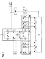
- Figure 1 shows a block and electronic diagram of the electronic integrated circuit according to the invention.
- Figure 1 shows the electronic integrated circuit comprising a current feedback differential amplifier DIFF with two differential signal inputs INP, INPI and outputs OUTP, OUTPI, the outputs connected to a digital feedback loop comprising an offset detector DET, an analog-to-digital converter AD, a control unit CU comprising two registers RL and RR whose outputs are connected to current compensating circuits OFL and OFR which are respectively connected to resistors R2 and R3 of the differential amplifier to close the loop.
- a current feedback differential amplifier DIFF with two differential signal inputs INP, INPI and outputs OUTP, OUTPI, the outputs connected to a digital feedback loop comprising an offset detector DET, an analog-to-digital converter AD, a control unit CU comprising two registers RL and RR whose outputs are connected to current compensating circuits OFL and OFR which are respectively connected to resistors R2 and R3 of the differential amplifier to close the loop.
- the differential amplifier DIFF also comprises two current sources I2 and I3 which are connected to the emitters of transistors Q0 and Q1 respectively.
- a way to implement current sources I2 and I3 is by means of a transistor stimulated by a voltage reference value and a resistor connected to the emitter of said transistor.
- I2 is controlled by reference voltage VR, transistor Q2 and resistor R2
- current source I3 is controlled by reference voltage VR, transistor Q3 and resistor R3.
- reference voltage VR Assuming a fixed value for reference voltage VR, the value of the current sources I2 and I3 will depend on the resistance connected to the emitter of Q2 and Q3 respectively.
- the invention proposes a digital compensating loop which modifies the values of currents I2 and I3 accordingly so that variations in current I0 and I1 of the ideal values are compensated in a way such that the DC offset voltage between outputs OUTP and OUTPI is maintained zero.
- currents I2 and I3 will depend on the resistance connected to the emitter of Q2 and Q3 respectively.
- the resistance value can be modified by current compensating circuits OFL and OFR, which in a preferred embodiment of the invention are realized by a plurality of NMOS transistors M 0 to M N and M N+1 to M 2N+1 , connected in parallel to resistors R2 and R3 respectively.
- the NMOS transistors when activated by applying a DC voltage act as a resistance connected in parallel to resistors R2 and R3, thus modifying the equivalent resistance seen at the emitter of transistors Q2 and Q3.
- a digital control unit CU is in charge of implementing the algorithm by which the transistors M 0 to M 2N+1 shall be activated/deactivated.
- the control unit CU receives information from the digital to analog converter AD about the DC offset voltage value which is present between the outputs OUTP and OUTPI of the differential amplifier DIFF.
- the CU reads this value and actuates on registers RR and RL which in turn activate/deactivate the corresponding transistors of the current compensating circuits OFL and OFR.
- One way of activating the transistors may follow an iterative process by which the value of the equivalent resistance is halved in every iteration until the DC offset voltage at the output of the differential amplifier reaches zero. Also the symmetric approach, that is, by doubling the value of the equivalent resistance in every iteration, may be followed. Another approach to activate the transistors may be used so that the value of the equivalent resistance is iteratively decremented/incremented by small values in a step-wise manner. Instead of a control unit CU which follows a determined algorithm, also an up/down counter element could be used to stimulate the transistors M 0 to M 2N+1 to implement the small value decrement/increment approach.
Landscapes
- Engineering & Computer Science (AREA)
- Power Engineering (AREA)
- Amplifiers (AREA)
Priority Applications (1)
| Application Number | Priority Date | Filing Date | Title |
|---|---|---|---|
| EP03290587A EP1458090A1 (de) | 2003-03-10 | 2003-03-10 | Elektronische integrierte Schaltung mit einem Differenzverstärker und digitaler Gleichspannungsoffset-Kompensation |
Applications Claiming Priority (1)
| Application Number | Priority Date | Filing Date | Title |
|---|---|---|---|
| EP03290587A EP1458090A1 (de) | 2003-03-10 | 2003-03-10 | Elektronische integrierte Schaltung mit einem Differenzverstärker und digitaler Gleichspannungsoffset-Kompensation |
Publications (1)
| Publication Number | Publication Date |
|---|---|
| EP1458090A1 true EP1458090A1 (de) | 2004-09-15 |
Family
ID=32749004
Family Applications (1)
| Application Number | Title | Priority Date | Filing Date |
|---|---|---|---|
| EP03290587A Withdrawn EP1458090A1 (de) | 2003-03-10 | 2003-03-10 | Elektronische integrierte Schaltung mit einem Differenzverstärker und digitaler Gleichspannungsoffset-Kompensation |
Country Status (1)
| Country | Link |
|---|---|
| EP (1) | EP1458090A1 (de) |
Cited By (4)
| Publication number | Priority date | Publication date | Assignee | Title |
|---|---|---|---|---|
| DE102004045709B4 (de) * | 2004-09-21 | 2009-03-19 | Infineon Technologies Ag | Verfahren zur Einstellung eines Verstärkers und Verstärkerschaltung |
| CN101610071B (zh) * | 2008-06-19 | 2011-12-14 | 承景科技股份有限公司 | 前置放大器及其中校准偏移电压的方法 |
| CN110402541A (zh) * | 2017-02-03 | 2019-11-01 | 诺韦尔达公司 | 脉冲发生器 |
| CN116073769A (zh) * | 2023-03-21 | 2023-05-05 | 厦门优迅高速芯片有限公司 | 集成直流失调消除和切片阈值调整功能的二合一消除电路 |
Citations (5)
| Publication number | Priority date | Publication date | Assignee | Title |
|---|---|---|---|---|
| US3434069A (en) * | 1967-04-27 | 1969-03-18 | North American Rockwell | Differential amplifier having a feedback path including a differential current generator |
| US3868583A (en) * | 1970-08-06 | 1975-02-25 | Analog Devices Inc | High-performance solid-state amplifier system |
| US5550512A (en) * | 1994-06-15 | 1996-08-27 | Silicon Systems, Inc. | Method for offset voltage trim for automatic gain controls |
| US20010048344A1 (en) * | 2000-05-11 | 2001-12-06 | Martin Isken | Amplifier circuit with offset compensation, in particular for digital modulation devices |
| US6396339B1 (en) * | 2000-06-28 | 2002-05-28 | Texas Instruments Incorporated | Operational amplifier trim method with process and temperature error compensation |
-
2003
- 2003-03-10 EP EP03290587A patent/EP1458090A1/de not_active Withdrawn
Patent Citations (5)
| Publication number | Priority date | Publication date | Assignee | Title |
|---|---|---|---|---|
| US3434069A (en) * | 1967-04-27 | 1969-03-18 | North American Rockwell | Differential amplifier having a feedback path including a differential current generator |
| US3868583A (en) * | 1970-08-06 | 1975-02-25 | Analog Devices Inc | High-performance solid-state amplifier system |
| US5550512A (en) * | 1994-06-15 | 1996-08-27 | Silicon Systems, Inc. | Method for offset voltage trim for automatic gain controls |
| US20010048344A1 (en) * | 2000-05-11 | 2001-12-06 | Martin Isken | Amplifier circuit with offset compensation, in particular for digital modulation devices |
| US6396339B1 (en) * | 2000-06-28 | 2002-05-28 | Texas Instruments Incorporated | Operational amplifier trim method with process and temperature error compensation |
Cited By (7)
| Publication number | Priority date | Publication date | Assignee | Title |
|---|---|---|---|---|
| DE102004045709B4 (de) * | 2004-09-21 | 2009-03-19 | Infineon Technologies Ag | Verfahren zur Einstellung eines Verstärkers und Verstärkerschaltung |
| CN101610071B (zh) * | 2008-06-19 | 2011-12-14 | 承景科技股份有限公司 | 前置放大器及其中校准偏移电压的方法 |
| CN110402541A (zh) * | 2017-02-03 | 2019-11-01 | 诺韦尔达公司 | 脉冲发生器 |
| CN110402541B (zh) * | 2017-02-03 | 2023-12-22 | 诺韦尔达公司 | 脉冲发生器 |
| US11874393B2 (en) | 2017-02-03 | 2024-01-16 | Novelda As | Pulse generator |
| CN116073769A (zh) * | 2023-03-21 | 2023-05-05 | 厦门优迅高速芯片有限公司 | 集成直流失调消除和切片阈值调整功能的二合一消除电路 |
| CN116073769B (zh) * | 2023-03-21 | 2023-08-11 | 厦门优迅高速芯片有限公司 | 集成直流失调消除和切片阈值调整功能的二合一消除电路 |
Similar Documents
| Publication | Publication Date | Title |
|---|---|---|
| JP3234293B2 (ja) | デジタル利得設定を備えたモノリシック集積差動増幅器 | |
| US8127603B2 (en) | Physical quantity sensor | |
| US20020180520A1 (en) | Variable gain amplifier | |
| EP0534007B1 (de) | Differenzverstärkeranordnung | |
| NL193076C (nl) | Versterkerregelketen. | |
| EP4385127A1 (de) | Verstärker mit variabler verstärkung und temperaturkompensierter verstärkung | |
| US5675290A (en) | Microwave amplifier circuit | |
| US6819170B1 (en) | Apparatus for sensing differential voltages with high common-mode levels | |
| EP1116324A1 (de) | Differenzverstärker mit verstärkerlinearisierung durch transkonduktanzkompensation | |
| US4000474A (en) | Signal amplifier circuit using a field effect transistor having current unsaturated triode vacuum tube characteristics | |
| US5115206A (en) | Merged differential amplifier and current source | |
| US6538513B2 (en) | Common mode output current control circuit and method | |
| US4536717A (en) | Compensated inverting/noninverting differential amplifier | |
| US4829263A (en) | High speed instrumentation amplifier with minimized offset voltage and drift | |
| JPH09232881A (ja) | カレントミラー回路および信号処理回路 | |
| US4757275A (en) | Wideband closed loop amplifier | |
| JPH031844B2 (de) | ||
| EP0129936B1 (de) | Stromquellenschaltungsvorrichtung | |
| EP0388890B1 (de) | Reaktanzsteuerschaltung mit einem Gleichstromverstärker zur Minimalisierung der Änderung eines Referenz-Reaktanzwertes | |
| US6404285B1 (en) | Transistor amplifier that accommodates large input signals | |
| US20200336109A1 (en) | Broadband driver with extended linear output voltage | |
| US6448853B1 (en) | Distortion improvement in amplifiers | |
| JPH0522159A (ja) | 高周波電力増幅器の出力レベル制御回路 | |
| JP3430415B2 (ja) | 差動増幅器 | |
| JPH08222968A (ja) | 増幅器 |
Legal Events
| Date | Code | Title | Description |
|---|---|---|---|
| PUAI | Public reference made under article 153(3) epc to a published international application that has entered the european phase |
Free format text: ORIGINAL CODE: 0009012 |
|
| AK | Designated contracting states |
Kind code of ref document: A1 Designated state(s): AT BE BG CH CY CZ DE DK EE ES FI FR GB GR HU IE IT LI LU MC NL PT SE SI SK TR |
|
| AX | Request for extension of the european patent |
Extension state: AL LT LV MK RO |
|
| AKX | Designation fees paid | ||
| REG | Reference to a national code |
Ref country code: DE Ref legal event code: 8566 |
|
| STAA | Information on the status of an ep patent application or granted ep patent |
Free format text: STATUS: THE APPLICATION IS DEEMED TO BE WITHDRAWN |
|
| 18D | Application deemed to be withdrawn |
Effective date: 20050316 |