EP1460582A1 - Dispositif et procede de traitement d'image - Google Patents
Dispositif et procede de traitement d'image Download PDFInfo
- Publication number
- EP1460582A1 EP1460582A1 EP02788790A EP02788790A EP1460582A1 EP 1460582 A1 EP1460582 A1 EP 1460582A1 EP 02788790 A EP02788790 A EP 02788790A EP 02788790 A EP02788790 A EP 02788790A EP 1460582 A1 EP1460582 A1 EP 1460582A1
- Authority
- EP
- European Patent Office
- Prior art keywords
- processing
- data
- filtering
- texture
- circuit
- Prior art date
- Legal status (The legal status is an assumption and is not a legal conclusion. Google has not performed a legal analysis and makes no representation as to the accuracy of the status listed.)
- Withdrawn
Links
Images






Classifications
-
- G—PHYSICS
- G06—COMPUTING OR CALCULATING; COUNTING
- G06T—IMAGE DATA PROCESSING OR GENERATION, IN GENERAL
- G06T15/00—Three-dimensional [3D] image rendering
- G06T15/04—Texture mapping
-
- G—PHYSICS
- G06—COMPUTING OR CALCULATING; COUNTING
- G06T—IMAGE DATA PROCESSING OR GENERATION, IN GENERAL
- G06T1/00—General purpose image data processing
- G06T1/20—Processor architectures; Processor configuration, e.g. pipelining
-
- G—PHYSICS
- G06—COMPUTING OR CALCULATING; COUNTING
- G06F—ELECTRIC DIGITAL DATA PROCESSING
- G06F15/00—Digital computers in general; Data processing equipment in general
- G06F15/16—Combinations of two or more digital computers each having at least an arithmetic unit, a program unit and a register, e.g. for a simultaneous processing of several programs
-
- G—PHYSICS
- G06—COMPUTING OR CALCULATING; COUNTING
- G06F—ELECTRIC DIGITAL DATA PROCESSING
- G06F17/00—Digital computing or data processing equipment or methods, specially adapted for specific functions
- G06F17/10—Complex mathematical operations
-
- G—PHYSICS
- G06—COMPUTING OR CALCULATING; COUNTING
- G06T—IMAGE DATA PROCESSING OR GENERATION, IN GENERAL
- G06T15/00—Three-dimensional [3D] image rendering
- G06T15/005—General purpose rendering architectures
-
- G—PHYSICS
- G06—COMPUTING OR CALCULATING; COUNTING
- G06T—IMAGE DATA PROCESSING OR GENERATION, IN GENERAL
- G06T17/00—Three-dimensional [3D] modelling for computer graphics
Definitions
- the present invention relates to an image processing apparatus and method thereof wherein a plurality of processing devices share processing data to perform parallel processing.
- First is a parallel processing method by area division
- second is a parallel processing method at a primitive level
- third is a parallel processing method at a pixel level.
- the above classification is based on the particle size of the parallel processing.
- the particle size of the area division parallel processing is the roughest, while the particle size of the pixel level parallel processing is the finest.
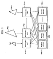
- FIG. 1 A view conceptually showing parallel processing at the primitive level is shown in FIG. 1.
- PM0 to PMn-1 indicate different primitives
- PU0 to PUn-1 indicate processing units
- MM0 to MMn-1 indicate memory modules.
- FIG. 2 is a view conceptually showing parallel processing at the primitive level based on the technique of parallel processings at the pixel level.
- pixels are generated in units of rectangular areas referred to as "pixel stamps PS" comprised of pixels arrayed in a 2 x 8 matrix.
- a total of eight pixel stamps from the pixel stamp PS0 to the pixel stamp PS7 are generated.
- a maximum of 16 pixels included in these pixel stamps PS0 to PS7 are simultaneously processed.
- This technique has an efficiency in parallel processing better by the amount of fineness of the particle size in comparison with the other techniques.
- DDA digital differential analyzer
- texture data is read out from a memory (ST2), sub-word reallocation is performed (ST3), then the data is globally distributed to the processing units by a crossbar circuit (ST4).
- texture filtering is performed (ST5).
- the processing units PU0 to PU3 perform four-neighbor interpolation or other filtering by using read texture data and a decimal fraction obtained when calculating a (u, v) address.
- processing at the pixel level is performed, specifically, texture data after the filtering and various types of data after rasterization are used for operations on pixel units (ST5).
- pixel data passing various types of tests in the processing at the pixel level is drawn in a frame buffer and Z-buffer on the memory modules MM0 to MM3.
- memory access of the texture read system differs from memory access of the graphics generation system, therefore it is necessary to read data from a memory belonging to another module.
- an interconnect such as a crossbar circuit as described above is necessary.
- a related image processing apparatus globally distributes data to the processing units, then performs texture filtering, so there are the disadvantages that the amount of data globally distributed is large (for example, 4 Tbps), the crossbar circuit serving as the global bus becomes large in size, and an increase in the speed of processing is obstructed from the viewpoint of interconnect delay etc.
- An object of the present invention is to provide an image processing apparatus and method thereof that can achieve a reduction in the size of a crossbar circuit and achieve an increase in speed of processing.
- a first aspect of the present invention is an image processing apparatus in which a plurality of processing modules share processing data to perform parallel processing, wherein: the plurality of processing modules each comprise: a memory module storing at least data relating to filtering, a processing circuit for obtaining data for filtering and performing assigned processing determined in advance by corresponding memory interleaving based on the processing data, a first operation processing element for performing operation processing in pixel units based on assigned processing data and data after filtering obtained at said processing circuit, and a second operation processing element for performing filtering based on the data for filtering obtained by said processing circuit and the data relating to filtering stored in said memory module and receiving operation processing data from the first operation processing element, then drawing the operation processed data to the memory module and further comprising a crossbar circuit which is a global bus for connecting a plurality of first operation processing elements and a plurality of second operation processing elements of said processing modules, supplying data for filtering obtained by said processing circuit in each processing module to a second operation processing element in the same processing module,
- the processing circuit of each processing module comprises a means for adjusting time so that the processing time of the assigned data becomes equal to time when the data after filtering is supplied to the first operation processing element.
- a second aspect of the present invention is an image processing method in which a plurality of processing modules share processing data to perform parallel processing: obtaining data for filtering and performing assigned process determined in advance by corresponding memory interleaving based on the processing data in each processing module; performing filtering based on the obtained data for filtering and data relating to filtering stored in a memory module; supplying data after filtering in each processing module, through a global bus, to a predetermined processing module; and performing operation processing in pixel unit based on the obtained assigned processing data and the data after filtering, and drawing the operation processed data to said memory module, in a processing module receiving the data after filtering.
- the method further comprises a step of adjusting each processing module time so that processing time of the assigned data becomes equal to time when the data after filtering is supplied.
- the processing requiring the filtering is processing relating to texture.
- the above parallel processing is parallel processing at the pixel level.
- the setup circuit performs an operation on the vertex data, sets up a primitive, and outputs the assigned texture's worth of setup information to the processing modules.
- the processing circuit of each processing module calculates for example the DDA parameters, specifically the inclination etc. of various types of data (Z, texture coordinates, colors, etc.) and other DDA parameters required for rasterization based on information from the setup circuit.
- each processing circuit judges whether for example a triangle is its assigned area based on the parameter data and, when its assigned area, performs rasterization.
- each processing circuit calculates the MipMap level by calculating the LOD and calculates the (u, v) address calculation for texture access.
- each processing circuit outputs the obtained texture coordinates and address information for texture access etc. to the second operation processing element.
- each processing circuit supplies the color and other information other than the texture obtained to the first operation processing element.
- each processing module receives coordinate data and address data relating to texture supplied from the processing circuit, reads out the texture data from memory module, and performs four-neighbor interpolation or other texture filtering using the read texture data and a decimal fraction obtained at the time of calculation of the (u, v) address.
- the texture data after filtering from a second operation processing element is supplied via the crossbar circuit to for example the first operation processing element of the processing module having a frame buffer corresponding to a stamp.
- the first operation processing element of a processing module performs processing at the pixel level based on data other than the texture information supplied from the processing circuit and data after texture filtering by the second operation processing element of a processing module received through the crossbar circuit and outputs the result to the second operation processing element.
- the second operation processing element receives the result of processing at the pixel level supplied from the first operation processing element and draws the pixel data passing various types of tests in the processing at the pixel level in the memory module.
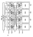
- FIG. 4 is a block diagram of the configuration of an embodiment of an image processing apparatus according to the present invention.
- An image processing apparatus 10 has, as shown in FIG. 4, a setup circuit 11, processing modules 12-0 to 12-3, and a crossbar circuit 13.
- processing modules 12-0 to 12-3 are connected in parallel to a setup circuit 11.
- a plurality of processing modules 12-0 to 12-3 share processing data to perform parallel processing.
- the setup circuit 11 controls the transfer of data with a CPU and an external memory and the transfer of data with the processing modules 12-0 to 12-3, performs operations on the vertex data, sets up one primitive, and outputs the assigned texture's worth of setup information to the processing modules 12-0 to 12-3.
- the setup circuit 11 performs a pervertex operation when data is input.
- the processing module 12-0 has a DDA (digital differential analyzer) circuit 121-0 as a processing circuit, a first operation processing element (operation processing element 1) 122-0, a second operation processing element (operation processing element 2) 123-0, and a memory module (MEM) 124-0 formed by a DRAM for example.
- DDA digital differential analyzer
- the processing module 12-1 has a DDA circuit 121-1 as a processing circuit, a first operation processing element (operation processing element 1) 122-1, a second operation processing element (operation processing element 2) 123-1, and a memory module (MEM) 124-1 formed by a DRAM for example.
- the processing module 12-2 has a DDA circuit 121-2 as a processing circuit, a first operation processing element (operation processing element 1) 122-2, a second operation processing element (operation processing element 2) 123-2, and a memory module (MEM) 124-2 formed by a DRAM for example.
- the processing module 12-3 has a DDA circuit 121-3 as a processing circuit, a first operation processing element (operation processing element 1) 122-3, a second operation processing element (operation processing element 2) 123-3, and a memory module (MEM) 124-3 formed by a DRAM for example.
- the first operation processing elements 122-0 to 122-3 and the second operation processing elements 123-0 to 123-3 in the processing modules 12-0 to 12-3, as described in detail later, are connected to each other via the crossbar circuit 13.
- FIG. 5 is a view of the basic architecture and a processing flow of an image processing apparatus according to the present embodiment. Note that in FIG. 5, arrows with circles indicate the flow of data relating to texture and arrows without circles indicate the flow of data relating to pixels.
- the memory modules 124-0 to 124-3 are interleaved to predetermined sizes, for example, 4 x 4 rectangle area units.
- a so-called frame buffer is interleaved to all memory modules and texture memories are dispersed in the memory modules 124-0 to 124-3.
- the DDA circuit 121-0 in the processing module 12-0 calculates DDA parameters based on information from the setup circuit 11.
- the DDA circuit 121-0 judges, based on the parameter data, whether a triangle for example is in an assigned area for the circuit to process and, when in the area, performs rasterization.
- the triangle judges whether the triangle belongs to area assigned to it, for example, an area interleaved by 4 x 4 pixel rectangle area units, and, when belonging to it, rasterizes various types of data (Z, texture coordinates, colors, etc.).
- the generated unit is 2 x 2 pixels per cycle per local module.
- This processing stage includes calculation of the MipMap level by calculation of the LOD (level of detail) and calculation of the (u, v) address for texture access.
- the DDA circuit 121-0 performs texture processing on the texture coordinates by a texture system DDA portion 1211, address information for texture access, etc. and outputs information relating to texture to the second operation processing element 123-0 via the first operation processing element 122-0 and the crossbar circuit 13.
- the DDA circuit 121-0 performs color and other processing other than texture by another DDA portion 1212 and outputs the result to the first operation processing element 122-0.
- each DDA circuit 121 (-0 to 3) is provided with a FIFO (first-in first-out) only at a data input side of the other DDA portion 1212 and adjusts the time considering the time of the filtering of the texture system.
- FIFO first-in first-out
- the texture system DDA portion 1211 generates data of the texture assigned to it for all pixels, while the other DDA portion 1212 generates only portions assigned by memory interleaving.
- the first operation processing element 122-0 performs processing at the pixel level (per-pixel operation) based on data other than the texture information supplied from the DDA circuit 121-0 and data after texture filtering by the second operation processing elements 123-0 to 123-3 of the processing modules 12-0 to 12-3 received through the crossbar circuit 13 and outputs the results to the second operation processing element 123-0 via the crossbar circuit 13.
- the texture data after filtering and the various types of data after rasterization are used for operations on pixel units.
- the processing performed here corresponds to pixel-level lighting (per-pixel lighting) or other so-called pixel shader processing.
- the second operation processing element 123-0 receives coordinate data and address data relating to texture supplied from the DDA circuit 121-0, reads out the texture data from the memory module 124-0, performs texture filtering, and outputs the texture data after the filtering via the crossbar circuit 13 to either of the first operation processing elements 122-0 to 122-3 in processing modules having a frame buffer corresponding to a stamp.
- the second operation processing element 123-0 performs four-neighbor interpolation or other filtering by using the read texture data and a decimal fraction obtained at the time of calculation of the (u, v) address.
- the second operation processing element 123-0 receives a processing result of the pixel level supplied from the first operation processing element 122-0 and draws the pixel data passing various tests in the processing at the pixel level to the memory module 124-0.
- the DDA circuit 121-1 in the processing module 12-1 calculates DDA parameters, specifically inclination of various types of data (Z, texture coordinates, colors, etc.) and other DDA parameters necessary for rasterization based on information from the setup circuit 11.
- the DDA circuit 121-1 judges, based on the parameter data, whether a triangle for example is its assigned area and, when the assigned area, performs rasterization.
- the triangle judges whether the triangle is its assigned area, for example, whether it belongs in an area interleaved in 4 x 4 pixel rectangle area units and, when belonging, rasterizes various types of data (Z, texture coordinates, colors, etc.).
- the generated unit is 2 x 2 pixels per cycle per local module.
- This processing stage includes calculation of the MipMap level by calculation of the LOD (level of detail) and calculation of the (u, v) address for texture access.
- the DDA circuit 121-1 performs texture processing on the texture coordinates by a texture system DDA portion 1211, address information for texture access, etc. and outputs information relating to texture to the second operation processing element 123-1 via the first operation processing element 122-1 and the crossbar circuit 13.
- the DDA circuit 121-1 performs color and other processing other than texture by another DDA portion 1212 and outputs the result to the first operation processing element 122-1.
- the first operation processing element 122-1 performs processing at the pixel level (per-pixel operation) based on data other than the texture information supplied from the DDA circuit 121-1 and data after texture filtering by the second operation processing elements 123-0 to 123-3 of the processing modules 12-0 to 12-3 received through the crossbar circuit 13 and outputs the results to the second operation processing element 123-1 via the crossbar circuit 13.
- the texture data after filtering and the various types of data after rasterization are used for operations on pixel units.
- the processing performed here corresponds to pixel-level lighting or other so-called pixel shader processing.
- the second operation processing element 123-1 receives coordinate data and address data relating to texture supplied from the DDA circuit 121-1, reads out the texture data from the memory module 124-1, performs texture filtering, and outputs the texture data after the filtering via the crossbar circuit 13 to either of the first operation processing elements 122-0 to 122-3 in processing modules having a frame buffer corresponding to a stamp.
- the second operation processing element 123-1 performs four-neighbor interpolation or other filtering by using the read texture data and a decimal fraction obtained at the time of calculation of the (u, v) address.
- the second operation processing element 123-1 receives processing results of the pixel level supplied from the first operation processing element 122-1 and draws the pixel data passing various tests in the processing at the pixel level to the memory module 124-1.
- the DDA circuit 121-2 in the processing module 12-2 calculates DDA parameters, specifically inclination of various types of data (Z, texture coordinate, colors, etc.) or other DDA parameters necessary for rasterization based on information from the setup circuit 11.
- the DDA circuit 121-2 judges, based on the parameter data, whether a triangle for example is its assigned area and, when the assigned area, performs rasterization.
- the triangle judges whether the triangle is its assigned area, for example, whether it belongs in an area interleaved in 4 x 4 pixel rectangle area units and, when belonging, rasterizes various types of data (Z, texture coordinates, colors, etc.).
- the generated unit is 2 x 2 pixels per cycle per local module.
- This processing stage includes calculation of the MipMap level by calculation of the LOD (level of detail) and calculation of the (u, v) address for texture access.
- the DDA circuit 121-2 performs texture processing on the texture coordinates by a texture system DDA portion 1211, address information for texture access, etc. and outputs information relating to texture to the second operation processing element 123-2 via the first operation processing element 122-2 and the crossbar circuit 13.
- the DDA circuit 121-2 performs color and other processing other than texture by another DDA portion 1212 and outputs the result to the first operation processing element 122-2.
- the first operation processing element 122-2 performs processing at the pixel level (per-pixel operation) based on data other than the texture information supplied from the DDA circuit 121-2 and data after texture filtering by the second operation processing elements 123-0 to 123-3 of the processing modules 12-0 to 12-3 received through the crossbar circuit 13 and outputs the results to the second operation processing element 123-2 via the crossbar circuit 13.
- the texture data after filtering and the various types of data after rasterization are used for operations on pixel units.
- the processing performed here corresponds to pixel-level lighting or other so-called pixel shader processing.
- the second operation processing element 123-2 receives coordinate data and address data relating to texture supplied from the DDA circuit 121-2, reads out the texture data from the memory module 124-2, performs texture filtering, and outputs the texture data after the filtering via the crossbar circuit 13 to either of the first operation processing elements 122-0 to 122-3 in processing modules having a frame buffer corresponding to a stamp.
- the second operation processing element 123-2 performs four-neighbor interpolation or other filtering by using the read texture data and a decimal fraction obtained at the time of calculation of the (u, v) address.
- the second operation processing element 123-2 receives processing results of the pixel level supplied from the first operation processing element 122-2 and draws the pixel data passing various tests in the processing at the pixel level to the memory module 124-2.
- the DDA circuit 121-3 in the processing module 12-3 calculates DDA parameters, specifically inclination of various types of data (Z, texture coordinate, colors, etc.) or other DDA parameters necessary for rasterization based on information from the setup circuit 11.
- the DDA circuit 121-3 judges, based on the parameter data, whether a triangle for example is its assigned area and, when the assigned area, performs rasterization.
- the triangle judges whether the triangle is its assigned area, for example, whether it belongs in an area interleaved in 4 x 4 pixel rectangle area units and, when belonging, rasterizes various types of data (Z, texture coordinates, colors, etc.).
- the generated unit is 2 x 2 pixels per cycle per local module.
- This processing stage includes calculation of the MipMap level by calculation of the LOD (level of detail) and calculation of the (u, v) address for texture access.
- the DDA circuit 121-3 performs texture processing on the texture coordinates by a texture system DDA portion 1211, address information for texture access, etc. and outputs information relating to texture to the second operation processing element 123-3 via the first operation processing element 122-3 and the crossbar circuit 13.
- the DDA circuit 121-3 performs color and other processing other than texture by another DDA portion 1212 and outputs the result to the first operation processing element 122-3.
- the first operation processing element 122-3 performs processing at the pixel level (per-pixel operation) based on data other than the texture information supplied from the DDA circuit 121-3 and data after texture filtering by the second operation processing elements 123-0 to 123-3 of the processing modules 12-0 to 12-3 received through the crossbar circuit 13 and outputs the results to the second operation processing element 123-3 via the crossbar circuit 13.
- the texture data after filtering and the various types of data after rasterization are used for operations on pixel units.
- the processing performed here corresponds to pixel-level lighting or other so-called pixel shader processing.
- the second operation processing element 123-3 receives coordinate data and address data relating to texture supplied from the DDA circuit 121-3, reads out the texture data from the memory module 124-3, performs texture filtering, and outputs the texture data after the filtering via the crossbar circuit 13 to either of the first operation processing elements 122-0 to 122-3 in processing modules having a frame buffer corresponding to a stamp.
- the second operation processing element 123-3 performs four-neighbor interpolation or other filtering by using the read texture data and a decimal fraction obtained at the time of calculation of the (u, v) address.
- the second operation processing element 123-3 receives processing results of the pixel level supplied from the first operation processing element 122-3 and draws the pixel data passing various tests in the processing at the pixel level to the memory module 124-3.
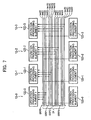
- FIG. 7 is a view of a concrete example of the configuration of a global bus system in a crossbar circuit according to the present embodiment.
- the crossbar circuit 13, as shown in FIG. 7, has four groups of a first to a fourth interconnect group GRP0 to GRP3, four texture lines forming one group.
- a first interconnect group GRP0 has four interconnects tex00 to tex03
- a second interconnect group GRP1 has four interconnects tex10 to tex13
- a third interconnect group GRP1 has four interconnects tex20 to tex23
- a fourth interconnect group GRP1 has four interconnects tex30 to tex33.
- a terminal of the second operation processing element 123-0 in the processing module 12-0 is connected to the interconnect tex00 in the first interconnect group GRP0, the interconnect tex10 in the second interconnect group GRP1, the interconnect tex20 in the third interconnect group GRP2, and the interconnect tex30 in the fourth interconnect group GRP3.
- a terminal of the second operation processing element 123-1 in the processing module 12-1 is connected to the interconnect tex01 in the first interconnect group GRP0, the interconnect tex11 in the second interconnect group GRP1, the interconnect tex21 in the third interconnect group GRP2, and the interconnect tex31 in the fourth interconnect group GRP3.
- a terminal of the second operation processing element 123-2 in the processing module 12-2 is connected to the interconnect tex02 in the first interconnect group GRP0, the interconnect tex12 in the second interconnect group GRP1, the interconnect tex22 in the third interconnect group GRP2, and the interconnect tex32 in the fourth interconnect group GRP3.
- a terminal of the second operation processing element 123-3 in the processing module 12-3 is connected to the interconnect tex03 in the first interconnect group GRP0, the interconnect tex13 in the second interconnect group GRP1, the interconnect tex23 in the third interconnect group GRP2, and the interconnect tex33 in the fourth interconnect group GRP3.
- the four interconnects tex00-tex03 in the first interconnect group GRP0 are connected to the terminal of the first operation processing element 122-0 in the processing module 12-0.
- the four interconnects tex10-tex13 in the second interconnect group GRP1 are connected to the terminal of the first operation processing element 122-1 in the processing module 12-1.
- the four interconnects tex20-tex23 in the third interconnect group GRP2 are connected to the terminal of the first operation processing element 122-2 in the processing module 12-2.
- the four interconnects tex30-tex33 in the fourth interconnect group GRP3 are connected to the terminal of the first operation processing element 122-3 in the processing module 12-3.
- Texture-filtering is performed by the second operation processing element 123 based on texture information from the texture DDA portion 1211 and texture data in the memory 124 (flow of data indicated by (1)).
- the texture data after the filtering is distributed by the crossbar circuit 13 to the first operation processing element 122 in a requested module (flow of data indicated by (2)).
- processing at the pixel level is performed in the first operation processing element 122 and the result is sent to the second operation processing element 123 via the crossbar circuit 13, thus the data is drawn in the memory module 124 (flow of data indicated by (3)).
- the setup circuit 11 performs an operation on the vertex data, sets up a primitive, and outputs the assigned texture's worth of setup information to the processing modules 12-0 to 12-3.
- the DDA circuits 121-0 to 121-3 in the processing modules 12-0 to 12-3 calculate DDA parameters, specifically inclination of various types of data (Z, texture coordinates, colors, etc.) or other DDA parameters necessary for rasterization based on information from the setup circuit 11.
- the DDA circuits 121-0 to 121-3 judge, based on the parameter data, whether for example a triangle for is its assigned area and, when its assigned area, performs rasterization.
- the DDA circuits 121-0 to 121-3 calculate the mipmap level by calculating the LOD and calculates the (u, v) address calculation for texture access.
- the DDA circuits 121-0 to 121-3 output texture coordinates obtained by the texture system DDA portion 1211 and address information for texture access etc. to the second operation processing elements 123-0 to 123-3 via the first operation processing elements 122-0 to 122-3 and the crossbar circuit 13.
- the DDA circuits 121-0 to 121-3 supply color and other information other than texture obtained by the other DDA portion 1212 to the first operation processing elements 122-0 to 122-3.
- the second operation processing elements 123-0 to 123-3 in the processing modules 12-0 to 12-3 receive coordinate data and address data relating to texture supplied from the DDA circuits 121-0 to 121-3, reads out texture data from the memory modules 124-0 to 124-3, then performs four-neighbor interpolation or other texture filtering using the read texture data and a decimal fraction obtained by calculation of the (u, v) address.
- the texture data after the filtering from the second operation processing elements 123-0 to 123-3 are supplied via the crossbar circuit 13 to the first operation processing element 122-1 in, for example, the processing module 12-1 having a frame buffer corresponding to a stamp.
- the first operation processing element 122-1 in the processing module 12-1 performs processing at the pixel level based on data other than texture information supplied from the DDA circuit 121-1 and data after texture filtering by the second operation processing elements 123-0 to 123-3 of the processing modules 12-0 to 12-3 received via the crossbar circuit 13 and outputs the results to the second operation processing element 123-1.
- the second operation processing element 123-1 receives the processing results at the pixel level supplied by the first operation processing element 122-1 and draws the pixel data passing various types of tests in the processing at the pixel level in the memory module 124-1.
- the present embodiment performs DDA processing (ST11), then reads out texture data from a memory (ST12), performs sub-word reallocation processing (ST13), then performs texture filtering (ST14), then globally distributes data by the crossbar circuit 13 to a first operation processing element of each processing module (ST15), then performs processing at the pixel level, specifically uses the texture data after filtering and the various types of data after rasterization to perform operations by pixel units and draws the pixel data passing the various types of tests in the processing at the pixel level to a frame buffer on a memory module (ST16), so can exhibit the following effects.
- the crossbar circuit 13 serving as a global bus can be made small in size.
- an image processing apparatus and method thereof according to the present invention can reduce the number of interconnects of a crossbar circuit and make the circuit small in size when a plurality of processing apparatuses share processing data to perform parallel processing.
- the design is easy and the interconnect cost and interconnect delay can be reduced, so the invention can be applied to a graphics LSI etc.
Landscapes
- Engineering & Computer Science (AREA)
- Physics & Mathematics (AREA)
- Theoretical Computer Science (AREA)
- General Physics & Mathematics (AREA)
- Computer Graphics (AREA)
- Software Systems (AREA)
- Mathematical Physics (AREA)
- Computer Hardware Design (AREA)
- General Engineering & Computer Science (AREA)
- Data Mining & Analysis (AREA)
- Computational Mathematics (AREA)
- Algebra (AREA)
- Mathematical Analysis (AREA)
- Mathematical Optimization (AREA)
- Geometry (AREA)
- Pure & Applied Mathematics (AREA)
- Databases & Information Systems (AREA)
- Image Processing (AREA)
- Image Generation (AREA)
- Multi Processors (AREA)
- Complex Calculations (AREA)
Applications Claiming Priority (3)
| Application Number | Priority Date | Filing Date | Title |
|---|---|---|---|
| JP2001379349 | 2001-12-12 | ||
| JP2001379349A JP3838086B2 (ja) | 2001-12-12 | 2001-12-12 | 画像処理装置およびその方法 |
| PCT/JP2002/012966 WO2003054800A1 (fr) | 2001-12-12 | 2002-12-11 | Dispositif et procede de traitement d'image |
Publications (2)
| Publication Number | Publication Date |
|---|---|
| EP1460582A1 true EP1460582A1 (fr) | 2004-09-22 |
| EP1460582A4 EP1460582A4 (fr) | 2008-11-19 |
Family
ID=19186757
Family Applications (1)
| Application Number | Title | Priority Date | Filing Date |
|---|---|---|---|
| EP02788790A Withdrawn EP1460582A4 (fr) | 2001-12-12 | 2002-12-11 | Dispositif et procede de traitement d'image |
Country Status (6)
| Country | Link |
|---|---|
| US (1) | US7437021B2 (fr) |
| EP (1) | EP1460582A4 (fr) |
| JP (1) | JP3838086B2 (fr) |
| KR (1) | KR100929746B1 (fr) |
| CN (1) | CN1282128C (fr) |
| WO (1) | WO2003054800A1 (fr) |
Families Citing this family (18)
| Publication number | Priority date | Publication date | Assignee | Title |
|---|---|---|---|---|
| US7079148B2 (en) * | 2003-07-23 | 2006-07-18 | Hewlett-Packard Development Company, L.P. | Non-volatile memory parallel processor |
| US8788996B2 (en) | 2003-09-15 | 2014-07-22 | Nvidia Corporation | System and method for configuring semiconductor functional circuits |
| US8732644B1 (en) | 2003-09-15 | 2014-05-20 | Nvidia Corporation | Micro electro mechanical switch system and method for testing and configuring semiconductor functional circuits |
| US8775997B2 (en) | 2003-09-15 | 2014-07-08 | Nvidia Corporation | System and method for testing and configuring semiconductor functional circuits |
| US8711161B1 (en) | 2003-12-18 | 2014-04-29 | Nvidia Corporation | Functional component compensation reconfiguration system and method |
| JP2005234727A (ja) * | 2004-02-18 | 2005-09-02 | Toshiba Corp | 画像処理装置、画像処理システムおよび画像処理方法 |
| US7091982B2 (en) * | 2004-05-14 | 2006-08-15 | Nvidia Corporation | Low power programmable processor |
| KR100868396B1 (ko) * | 2004-08-26 | 2008-11-11 | 인텔 코오퍼레이션 | 기하 이미지 분할을 위한 그래픽 처리 시스템 및 방법 |
| US8723231B1 (en) | 2004-09-15 | 2014-05-13 | Nvidia Corporation | Semiconductor die micro electro-mechanical switch management system and method |
| US8711156B1 (en) | 2004-09-30 | 2014-04-29 | Nvidia Corporation | Method and system for remapping processing elements in a pipeline of a graphics processing unit |
| JP2006202211A (ja) * | 2005-01-24 | 2006-08-03 | Fujitsu Ltd | 画像描画装置および画像描画方法 |
| JP4637640B2 (ja) * | 2005-05-16 | 2011-02-23 | 三菱電機株式会社 | 図形描画装置 |
| US8232991B1 (en) * | 2006-11-03 | 2012-07-31 | Nvidia Corporation | Z-test result reconciliation with multiple partitions |
| US8724483B2 (en) | 2007-10-22 | 2014-05-13 | Nvidia Corporation | Loopback configuration for bi-directional interfaces |
| US9331869B2 (en) | 2010-03-04 | 2016-05-03 | Nvidia Corporation | Input/output request packet handling techniques by a device specific kernel mode driver |
| DE112011105994B4 (de) * | 2011-12-21 | 2017-04-06 | Intel Corporation | Techniken und Verfahren für die Ratenregelung eines Anzeigedatenstroms |
| JP5993267B2 (ja) * | 2012-10-04 | 2016-09-14 | オリンパス株式会社 | 画像処理装置 |
| WO2016000129A1 (fr) * | 2014-06-30 | 2016-01-07 | Intel Corporation | Mécanisme de partition adaptatif avec forme de carreau arbitraire pour architecture gpu de reproduction par carreaux |
Family Cites Families (17)
| Publication number | Priority date | Publication date | Assignee | Title |
|---|---|---|---|---|
| JPH0348979A (ja) * | 1989-07-17 | 1991-03-01 | Nec Corp | 並列画像処理装置 |
| JP2858602B2 (ja) * | 1991-09-20 | 1999-02-17 | 三菱重工業株式会社 | パイプライン演算回路 |
| US5359674A (en) * | 1991-12-11 | 1994-10-25 | David Sarnoff Research Center, Inc. | Pyramid processor integrated circuit |
| JP2642039B2 (ja) * | 1992-05-22 | 1997-08-20 | インターナショナル・ビジネス・マシーンズ・コーポレイション | アレイ・プロセッサ |
| US5566284A (en) * | 1993-12-22 | 1996-10-15 | Matsushita Electric Industrial Co., Ltd. | Apparatus and method for mip-map generation using low-pass filtering based on resolution ratio |
| US5493643A (en) * | 1994-05-03 | 1996-02-20 | Loral Aerospace Corp. | Image generator architecture employing tri-level fixed interleave processing and distribution buses |
| JPH08335273A (ja) * | 1995-06-08 | 1996-12-17 | Hitachi Denshi Ltd | 画像発生装置 |
| US5956744A (en) * | 1995-09-08 | 1999-09-21 | Texas Instruments Incorporated | Memory configuration cache with multilevel hierarchy least recently used cache entry replacement |
| US5638533A (en) * | 1995-10-12 | 1997-06-10 | Lsi Logic Corporation | Method and apparatus for providing data to a parallel processing array |
| JP3645024B2 (ja) * | 1996-02-06 | 2005-05-11 | 株式会社ソニー・コンピュータエンタテインメント | 描画装置及び描画方法 |
| US6104842A (en) * | 1996-06-10 | 2000-08-15 | Integrated Device Technology, Inc. | Geometry processing of digital video models and images |
| US6236405B1 (en) * | 1996-07-01 | 2001-05-22 | S3 Graphics Co., Ltd. | System and method for mapping textures onto surfaces of computer-generated objects |
| EP0825550A3 (fr) | 1996-07-31 | 1999-11-10 | Texas Instruments Incorporated | Système et méthode d'impression à processeurs multiples |
| US6130967A (en) * | 1997-07-03 | 2000-10-10 | Tri Path Imaging, Inc. | Method and apparatus for a reduced instruction set architecture for multidimensional image processing |
| US6452603B1 (en) * | 1998-12-23 | 2002-09-17 | Nvidia Us Investment Company | Circuit and method for trilinear filtering using texels from only one level of detail |
| US6661424B1 (en) * | 2000-07-07 | 2003-12-09 | Hewlett-Packard Development Company, L.P. | Anti-aliasing in a computer graphics system using a texture mapping subsystem to down-sample super-sampled images |
| US6763150B1 (en) * | 2000-08-29 | 2004-07-13 | Freescale Semiconductor, Inc. | Image processing system with multiple processing units |
-
2001
- 2001-12-12 JP JP2001379349A patent/JP3838086B2/ja not_active Expired - Fee Related
-
2002
- 2002-12-11 US US10/467,543 patent/US7437021B2/en not_active Expired - Fee Related
- 2002-12-11 WO PCT/JP2002/012966 patent/WO2003054800A1/fr not_active Ceased
- 2002-12-11 KR KR1020037010540A patent/KR100929746B1/ko not_active Expired - Fee Related
- 2002-12-11 EP EP02788790A patent/EP1460582A4/fr not_active Withdrawn
- 2002-12-11 CN CNB02804889XA patent/CN1282128C/zh not_active Expired - Fee Related
Also Published As
| Publication number | Publication date |
|---|---|
| KR100929746B1 (ko) | 2009-12-03 |
| US7437021B2 (en) | 2008-10-14 |
| CN1491402A (zh) | 2004-04-21 |
| WO2003054800A1 (fr) | 2003-07-03 |
| EP1460582A4 (fr) | 2008-11-19 |
| US20040196290A1 (en) | 2004-10-07 |
| CN1282128C (zh) | 2006-10-25 |
| KR20040073280A (ko) | 2004-08-19 |
| JP3838086B2 (ja) | 2006-10-25 |
| JP2003178293A (ja) | 2003-06-27 |
Similar Documents
| Publication | Publication Date | Title |
|---|---|---|
| EP1460582A1 (fr) | Dispositif et procede de traitement d'image | |
| US7333115B2 (en) | Image processing apparatus and method thereof | |
| US8941653B2 (en) | Order-preserving distributed rasterizer | |
| US6940512B2 (en) | Image processing apparatus and method of same | |
| US9070213B2 (en) | Tile based precision rasterization in a graphics pipeline | |
| US8704836B1 (en) | Distributing primitives to multiple rasterizers | |
| CA2480081C (fr) | Infographie 3d evolutive haute performance | |
| US9449410B2 (en) | Intra-frame timestamps for tile-based rendering | |
| US7109987B2 (en) | Method and apparatus for dual pass adaptive tessellation | |
| US8395619B1 (en) | System and method for transferring pre-computed Z-values between GPUs | |
| JP2007179563A (ja) | グラフィックス処理の最適化方法 | |
| US8933945B2 (en) | Dividing work among multiple graphics pipelines using a super-tiling technique | |
| US9471952B2 (en) | Method and system for coordinated data execution using a primary graphics processor and a secondary graphics processor | |
| TWI498850B (zh) | 訊框緩衝區歸併的方法、電腦可讀取記憶體、與電腦系統 | |
| US8228337B1 (en) | System and method for temporal load balancing across GPUs | |
| US8427487B1 (en) | Multiple tile output using interface compression in a raster stage | |
| US11055820B2 (en) | Methods, apparatus and processor for producing a higher resolution frame | |
| US6473091B1 (en) | Image processing apparatus and method | |
| US8427474B1 (en) | System and method for temporal load balancing across GPUs | |
| JP4000880B2 (ja) | 画像処理装置およびその方法 | |
| EP1308899A2 (fr) | Appareil de traitement d'image | |
| US7916151B1 (en) | Partial texture loads | |
| JPH09270024A (ja) | 情報処理装置 | |
| US7898543B1 (en) | System and method for optimizing texture retrieval operations |
Legal Events
| Date | Code | Title | Description |
|---|---|---|---|
| PUAI | Public reference made under article 153(3) epc to a published international application that has entered the european phase |
Free format text: ORIGINAL CODE: 0009012 |
|
| 17P | Request for examination filed |
Effective date: 20030716 |
|
| AK | Designated contracting states |
Kind code of ref document: A1 Designated state(s): AT BE BG CH CY CZ DE DK EE ES FI FR GB GR IE IT LI LU MC NL PT SE TR |
|
| AX | Request for extension of the european patent |
Extension state: AL LT LV MK RO |
|
| A4 | Supplementary search report drawn up and despatched |
Effective date: 20081020 |
|
| 17Q | First examination report despatched |
Effective date: 20090204 |
|
| STAA | Information on the status of an ep patent application or granted ep patent |
Free format text: STATUS: THE APPLICATION IS DEEMED TO BE WITHDRAWN |
|
| 18D | Application deemed to be withdrawn |
Effective date: 20120703 |