EP1463120A2 - Festkörperbildaufnahmevorrichtung und Verfahren zur Herstellung - Google Patents
Festkörperbildaufnahmevorrichtung und Verfahren zur Herstellung Download PDFInfo
- Publication number
- EP1463120A2 EP1463120A2 EP04251592A EP04251592A EP1463120A2 EP 1463120 A2 EP1463120 A2 EP 1463120A2 EP 04251592 A EP04251592 A EP 04251592A EP 04251592 A EP04251592 A EP 04251592A EP 1463120 A2 EP1463120 A2 EP 1463120A2
- Authority
- EP
- European Patent Office
- Prior art keywords
- solid
- state imaging
- adhesive
- spacer
- transfer member
- Prior art date
- Legal status (The legal status is an assumption and is not a legal conclusion. Google has not performed a legal analysis and makes no representation as to the accuracy of the status listed.)
- Granted
Links
Images



Classifications
-
- H—ELECTRICITY
- H10—SEMICONDUCTOR DEVICES; ELECTRIC SOLID-STATE DEVICES NOT OTHERWISE PROVIDED FOR
- H10F—INORGANIC SEMICONDUCTOR DEVICES SENSITIVE TO INFRARED RADIATION, LIGHT, ELECTROMAGNETIC RADIATION OF SHORTER WAVELENGTH OR CORPUSCULAR RADIATION
- H10F39/00—Integrated devices, or assemblies of multiple devices, comprising at least one element covered by group H10F30/00, e.g. radiation detectors comprising photodiode arrays
- H10F39/80—Constructional details of image sensors
- H10F39/804—Containers or encapsulations
-
- H—ELECTRICITY
- H10—SEMICONDUCTOR DEVICES; ELECTRIC SOLID-STATE DEVICES NOT OTHERWISE PROVIDED FOR
- H10F—INORGANIC SEMICONDUCTOR DEVICES SENSITIVE TO INFRARED RADIATION, LIGHT, ELECTROMAGNETIC RADIATION OF SHORTER WAVELENGTH OR CORPUSCULAR RADIATION
- H10F39/00—Integrated devices, or assemblies of multiple devices, comprising at least one element covered by group H10F30/00, e.g. radiation detectors comprising photodiode arrays
- H10F39/011—Manufacture or treatment of image sensors covered by group H10F39/12
-
- H—ELECTRICITY
- H10—SEMICONDUCTOR DEVICES; ELECTRIC SOLID-STATE DEVICES NOT OTHERWISE PROVIDED FOR
- H10F—INORGANIC SEMICONDUCTOR DEVICES SENSITIVE TO INFRARED RADIATION, LIGHT, ELECTROMAGNETIC RADIATION OF SHORTER WAVELENGTH OR CORPUSCULAR RADIATION
- H10F39/00—Integrated devices, or assemblies of multiple devices, comprising at least one element covered by group H10F30/00, e.g. radiation detectors comprising photodiode arrays
- H10F39/10—Integrated devices
- H10F39/12—Image sensors
Definitions
- the present invention relates to a method for manufacturing a solid-state imaging device by use of wafer level chip size packaging technique, and a solid-state imaging device manufactured by such manufacturing method.
- a conventional solid-state imaging device is manufactured by the following steps. First, a solid-state imaging element chip, such as a charge coupled device (CCD) formed on a wafer, is die-bonded on a package formed from a ceramic, for instance. Then, after the terminals of the solid-state imaging element chip and the terminals of the package are electrically connected by bonding wires, a glass lid formed from a transparent glass is fixed to the package to seal the solid-state imaging element chip.
- CCD charge coupled device
- Small solid-state imaging device is preferable in terms of miniaturizing the digital camera and the small electric apparatus.
- a wafer level chip size packaging technique (hereinafter referred to as "wafer level CSP”) can package the solid-state imaging device without the packaging material.
- wafer level CSP a wafer level chip size packaging technique
- Japan Patent Laid-Open Publication (JP-A) No. 2002-231921 describes the solid-state imaging device, manufactured by the wafer level CSP technique, in which a spacer is bonded to the peripheral area of the upper surface of the solid-state imaging element chip.
- the cover glass is provided on the spacer to seal the solid-state imaging element chip.
- the solid-state imaging element chip has connection terminals on the upper, bottom or lateral surface.
- the solid-state imaging device In manufacturing the solid-state imaging device by the wafer level CSP technique, plural spacers are formed on the glass substrate as the cover glass. Then, after adhesives are applied to the edge surface of the spacers, the glass substrate is adhered to a wafer on which plural solid-state imaging element chips are formed. The wafer with the glass substrate is subject to dicing process to manufacture the solid-state imaging device.
- the spacer In bonding the spacer to the wafer, if the adhesives are flowed on the solid-state imaging element chip, the solid-state imaging device does not work properly because of noise interference caused by the flowed adhesive. Moreover, if the gap between the spacer and the wafer is not tightly sealed, the solid-state imaging device is damaged by cooling water during the dicing process. Thus, in order to increase productivity, the spacer must be tightly bonded to the wafer.
- the adhesives applied on the spacer must be thin and uniform in thickness over the applied area. Although a small amount of adhesive with high viscosity is dropped on the spacer by potting method according to the above publication, putting the adhesives on the spacer having the width less than 200 ⁇ m is technically difficult. Even if the spacer has the width more than 200 ⁇ m, dropping the adhesives on all bonded surfaces of the plural spacers takes too much time for the adhering process.
- the width of the frame-shaped spacer is necessary to be considered. If the width of the spacer is too large, an improper bonding will happen because of air remaining inside the adhesive. Moreover, large width spacer will make it difficult to decrease the size of the solid-state imaging device. Thus, the manufacture cost will increase because of the small number of solid-state imaging devices per wafer. On the other hand, if the width of the spacer is too narrow, the solid-state imaging device will be physically weak.
- An object of the present invention is to provide a method for manufacturing a solid-state imaging device that is capable of bonding the spacers properly to the solid-state imaging elements on the wafer.
- Another object of the present invention is to provide a solid-state imaging device that is manufactured by such manufacturing method.
- the solid-state imaging device is manufactured by use of a transfer member to transfer an adhesive to a frame-shaped spacer to be bonded to a wafer on which plural solid-state imaging elements area formed.
- the spacers are formed in a transparent substrate, and each of the spacers surrounds the solid-state imaging element.
- the transfer member, which the adhesive is applied to, is stuck to the spacers. After applying the pressure to the transparent substrate and the transfer member, the transfer member is released from the transparent substrate to transfer the adhesive layer on the spacer.
- the transfer member may be a rigid body such as a glass plate. It is also possible to form the transfer member from an elastic body, such as a flexible plastic film.
- the flexible film as the transfer member is preferably peeled off in such a manner that the angle between the transfer member and the transparent substrate is kept constant.
- the transfer member may have a ridge pattern or a recess pattern that is the same pattern as the spacers in the transparent substrate. It is also possible to apply a release agent, such as silicon, on the surface of the transfer member.
- the viscosity of the adhesive is preferably 0.1 Pa ⁇ s or more.
- the adhesive is applied to the transfer member by bar coating, blade coating or spin coating. In addition, it is preferable to apply air pressure or roller pressure to the transfer member and the transparent substrate.
- the viscosity of the adhesive at the time of transferring to the spacer is preferably 100 Pa ⁇ s to 10000 Pa ⁇ s .
- the thickness of the adhesive is 0.5 ⁇ m to 5 ⁇ m when the adhesive is activated.
- the spacer may be bonded to the wafer over the surface to which the adhesive is applied.
- the solid-state imaging device manufactured by the above methods, may have the following features.
- the solid-state imaging element and the inner surface of the spacer are separated by 50 ⁇ m to 100 ⁇ m over the whole edge of the solid-state imaging element.
- the width of the spacer is 100 ⁇ m to 500 ⁇ m. It is possible to form chamfer edges in the surface of the spacer to which the adhesive is applied. The surplus of the adhesive is contained in the space between the wafer and the chamfer edges.
- the adhesive is applied to the spacer by use of the transfer member with the adhesive, it is possible to apply thin adhesive on spacers evenly at a desired thickness. Thereby, the spacers are bonded properly to the wafer without forming a gap therebetween. It is also possible to prevent the adhesive from being flowed to the solid-state imaging element.
- a rigid body having high flatness as the transfer member makes it possible to control the thickness of the adhesive.
- the transfer member is deformed to fit the surface of the spacers.
- it is possible to facilitate precise control of the thickness of adhesive without ay effect by the difference in height of the spacers and the transparent substrate.
- the angle between the transfer member and the transparent substrate is kept constant while the transfer member is peeled off, it is possible to increase the uniformity of the adhesive on the spacers.
- a ridge pattern that is the same as the pattern of the spacers on the transfer member, it is possible to ensure to contact of the transfer member to the spacers.
- a recess pattern which is the same as the pattern of the spacers, makes it possible to control the thickness of the adhesive by adjusting the depth of the recess.
- a release agent on the surface of the transfer member increases the peelability of the adhesive, so the thickness of the adhesive on the spacer may be the same as the thickness of the adhesive on the transfer member. Moreover, since surface modification to the spacer increases the wettability to the adhesive, it is possible to apply the adhesive uniformly.
- the viscosity of the adhesive is low (0.1 Pa ⁇ s or more).
- the thickness of the adhesive it is possible to control the thickness of the adhesive easily.
- the adhesive is applied to the transfer member by bar coating, blade coating or spin coating, it is possible to apply the adhesive evenly with high precision at a low cost.
- the transfer member and the transparent substrate are uniformly pressed to each other over the whole bonded surfaces by air pressure or roller pressure.
- the thickness of the adhesive is 0.5 ⁇ m to 5 ⁇ m when the adhesive is activated, it is possible to reduce the amount of the adhesive to be flowed out of the spacer after bonding to the wafer. Such thickness of the adhesive does not generate a gap between the spacer and the wafer. Moreover, since the spacer is bonded to the wafer over the surface to which the adhesive is applied, it is possible to control the bonding strength by choosing the thickness of the spacer.
- the solid-state imaging element and the inner surface of the spacer are separated by 50 ⁇ m to 100 ⁇ m over the whole edge of the solid-state imaging element, so the flowed adhesive does not reach the solid-state imaging element.
- incident light reflected on the inner surface of the spacer does not reach the solid-state imaging element.
- the width of the spacer is 100 ⁇ m to 500 ⁇ m, it is possible to ensure even application of the adhesive. Moreover, it is possible to increase the strength of the spacer while preventing the increase in manufacture cost.
- the surplus adhesive is contained in the space between the wafer and the chamfer edges formed in the surface of the spacer to which the adhesive is applied, so the flowed adhesive does not reach the solid-state imaging element.
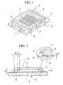
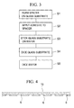
- FIGS. 1 and 2 respectively show the perspective and partial cross section of a solid-state imaging device of the wafer level CPS structure that is manufactured by the method according to the present invention.
- the solid-state imaging device 2 comprises a solid-state imaging element 3, a rectangular-shaped solid-state imaging element chip 5, a frame-shaped spacer 6 and a cover glass 7.
- the solid-state imaging element 3 is coupled to the solid-state imaging element chip 5 via plural terminals 4 formed on the solid-state imaging element chip 5.
- the spacer 6, bonded to the solid-state imaging element chip 5, surrounds the solid-state imaging element 3.
- the cover glass 7 is provided on the spacer 6 to seal the solid-state imaging element 3.
- the cover glass 7 is made from a transparent ⁇ -ray shielding glass for the purpose of protecting the photo-diodes of the CCD.
- the solid-state imaging element 3 is a charge coupled device (CCD). There are color filters and micro lenses on the CCD.
- the terminals 4 are formed on the solid-state imaging element chip 5 by printing a conductive material. Circuit patterns between the terminals 4 and the solid-state imaging element 3 are also formed by printing. After forming the solid-state imaging element 3 and the terminals 4 on a wafer, the solid-state imaging element chips 5 are separated by dicing process.
- the spacer 6 is formed from an inorganic material such as silicon.
- the width W of the spacer 6 is 100 ⁇ m to 500 ⁇ m, for instance.
- the height H of the spacer 6 is, for instance, 10 ⁇ m to 500 ⁇ m, and preferably 80 ⁇ m to 120 ⁇ m.
- An adhesive 12 to bond the solid-state imaging element chip 5 and the spacer has a thickness T2 of 0.5 ⁇ m to 5 ⁇ m.
- a frame-shaped surrounding area C is provided between the inner surface of the spacer 6 and the edge of the solid-state imaging element chip 5.
- the surrounding area C surrounds the whole edge of the solid-state imaging element chip 5 for the purpose of preventing incident light reflected on the inner surface of the spacer 6 from entering the solid-state imaging element chip 5.
- the surrounding area C is also effective in order not to affect the stress, generated at the interface between the solid-state imaging element chip 5 and the spacer 6, to the solid-state imaging element 3. Such stress is generated when a glass substrate having spacers 6 is pressed to the wafer as the base material of the solid-state imaging element chips 5 in bonding the spacer 6.
- the solid-state imaging element Because the solid-state imaging element generates much heat when the solid-state imaging device 3 is operated at a high clock rate or takes an image for a long exposure time, such stress is also generated because of the difference in thermal expansion rate of the spacer 6 and the solid-state imaging element chip 5.
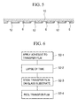
- the solid-state imaging device 2 is manufactured by the steps according to the flow chart of FIG. 3.
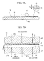
- plural spacers 6 are formed on a glass substrate 10 used as the cover glass 7, as shown in FIG. 4.
- the spacers 6 are formed by the following method, for example.
- an inorganic material film composed of an inorganic material such as silicon
- CVD chemical vapor deposition
- plural spacers 6 are formed from the inorganic material film by photo lithography, development, etching and so forth.
- the inorganic material film may be formed on the glass substrate 10 by bonding a silicon wafer to the glass substrate 10.
- an inorganic material may be directly printed on the glass substrate 10 to form the spacer 6.
- a thin adhesive 12 is uniformly applied on edge surfaces of the spacer 6, to be glued to the wafer, on the glass substrate 10.
- the adhesive 12 for gluing the spacer 6 to the wafer is required to prevent deformation upon activation, and to keep in water-tight manner.
- the adhesives 12 are room-temperature activated adhesives of epoxy resins, silicon resins, and so forth.
- the adhesives 12 preferably have viscosity V1 about 0.1 Pa ⁇ s to 10 Pa ⁇ s .
- Other types of adhesives, such as UV activated adhesives, visible light activated adhesives and heat activated adhesives may be used as the adhesive 12, if these adhesives yield the same effect.
- the adhesive 12 is applied to the spacers 6 by the steps S2-1 to S2-4, which are shown in FIGS. 6, 7A, 7B and 8.
- a transfer film 16 is laid on a flat work table 15, as shown in FIG. 7A.
- the work table 15 is made of glass with high flatness, for instance.
- the transfer film 16, used as a transfer member, is laid on the working table 15 by air suction or electrostatic chuck, such that the transfer film 16 neither have wrinkles nor shift the position on the working table 15.
- the transfer film 16 is a flat and thin film that is made of polyethylene terephthalate (PET).
- PET polyethylene terephthalate
- the transfer film 16 has a shape larger than the glass substrate 10.
- a coating bar 17 for bar coater applies the adhesive 12 uniformly on the transfer film 16 on the working table 15.
- the thickness T1 of the adhesive 12 on the transfer film 16 is 6 ⁇ m to 10 ⁇ m, preferably 8 ⁇ m. It is possible to utilize other type of coater, such as a blade coater and a spin coater.
- the manufacture process according to the embodiment includes a step S2-2 to leave the transfer film 16 for a predetermined time after the adhesive 12 is applied, so the viscosity of the adhesive 12 increases.
- the temperature and the predetermined time are adjusted such that the viscosity of the adhesive 12 increases to V2, for transfer to the spacer 6, from V1 that is the initial viscosity at the time of application to the transfer film 16.
- the viscosity V2 is 100 Pa ⁇ s to 10000 Pa ⁇ s, for instance, and preferably about 2000 Pa ⁇ s to about 3000 Pa ⁇ s.
- the adhesive 12 with low viscosity at the time of application to the transfer film 16, and by increasing the viscosity for transferring the adhesive 12 to the spacer, it is possible to control the thickness of the adhesive 12 precisely while keeping a high wettability to the spacer 6. Since the adhesive 12 with high viscosity does not flow easily, it is possible to handle the transfer film 16, and the glass substrate 10 easily after transfer of the adhesive 12. Moreover, if the adhesive 12 has high viscosity, it is possible to reduce the amount of the adhesive 12 squeezed out of the spacer 6 in bonding the spacers 6 onto the wafer 26.
- the spacer 6 may improve its wettability to the adhesive 12 by surface modification, such as application of plasma or ultraviolet rays.
- the glass substrate 10 is glued to the transfer film 16 by hand or by use of an alignment equipment.
- An example of the alignment equipment is depicted in FIG. 7B.
- the alignment equipment comprises a glass holder table 20 and a film holder table 21.
- the glass holder table 20 holds the glass substrate 10 by air suction through suction holes 20a.
- the film holder table 21 holds the transfer film 16 via a sponge 21b by air suction from suction holes 21a.
- the film holder table 21 is moveable up and down (vertical direction in the drawing) in the same manner as a well-known Z-axis movement table.
- the film holder table 21 holds the transfer film 16 on the sponge 21b after application of the adhesive 12, and moves upward to uniformly press the transfer film 16 onto the spacers 6 that is formed on the glass substrate 10.
- the sponge 21b needs to have enough strength to press the transfer film 16 firmly onto the spacer 6 without breaking the spacer 6.
- the glass substrate 10 is glued to the transfer film 16 since the film holder table 21 ensures the spacer 6 to contact to the adhesive 12 on the transfer film 16.
- the glass substrate 10 may be glued to the transfer film 16 by moving a pressure roller on the glass substrate 10.
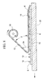
- a film peeling equipment used in this step comprises a working table 22, a winding roller 23 and a peeling guide 24.
- the working table 22 to hold the glass substrate 10 by air suction, for instance, is slidable horizontally by a table moving mechanism used for a well-known XY table.
- One end of the transfer film 16 is fixed to the winding roller 23.
- the peeling guide 24 comes in contact with the upper surface of the transfer film 16, and keeps the angle ⁇ between the transfer film 16 and the glass film 10 constant.
- the film peeling equipment starts to drive the winding roller 23 to wind the transfer film 16 at the same time as sliding the working table 22 to leftward in the drawing. Thereby, the transfer film 16 is peeled off from one end of the glass substrate 10. Since the shape of the rear surface of the transfer film 16 is regulated by the peeling guide, the angle ⁇ between the transfer film 16 and the glass film 10 becomes constant. Thus, the thickness of the transferred adhesive 12 becomes uniform. If the transfer film 16 is not large enough to engage the winding roller 23, an extension film is attached to one end of the transfer film 16 such that the transfer film 16 is fixed to the winding roller 23.
- the glass substrate 10 is bonded to the wafer 26 on which plural solid-state imaging elements 3 and the connecting terminals 4 are formed, as shown in FIG. 9A.
- the glass substrate 10 and the wafer 26 have the same size and shape (see FIG. 10).
- An alignment bonding equipment, used for bonding the glass substrate 10 to the wafer 26, comprises a bonding table 28 and positioning table 29.
- the bonding table 28 holds and positions the wafer 26 by air suction through air suction holes 28a.
- the positioning table 29 holds the glass substrate 10 by air suction through air suction holes 29a, and adjusts the position of the glass substrate 10 in the XY direction (horizontal direction) and the angle to fit the position and angle of the wafer 26.
- the positioning table 29 adjusts the position of the glass substrate 10 by use of orientation flat lines 26a, 10a of the wafer 26 and the glass substrate 10, and alignment marks that are properly formed in the wafer 26 and the glass substrate 10. After positioning, the positioning table 29 moves downward to stick the glass substrate 10 on the wafer 26. Then, pressure is applied to the whole surface of the glass substrate 10 at a relatively weak pressure so that the glass substrate 10 is provisionally bonded to the wafer 26. Note that the alignment bonding equipment for provisional bonding does not have the sponge used for the alignment equipment (see FIG. 7B), because the spacer 6 needs to be precisely positioned with respect to the solid-state imaging element 3 in bonding the glass substrate 10 to the wafer 26.
- the pressure bonding equipment comprises a bonding table 30 and a pressure table 33.
- the bonding table 30 holds the wafer 26 and the glass substrate 10 at a predetermined position by air suction through air suction holes 30a.
- the pressure table 33 provided above the bonding table 30, presses the glass substrate 10 at a predetermined uniform pressure via a sponge 33a. In order to ensure firm bonding, the pressure bonding equipment presses the glass substrate 10 and the wafer 26 for a predetermined time until the adhesive 12 is activated.
- the width W of the framed portion of the spacer 6 affects the strength and the condition in bonding between the spacer 6 and the wafer 26, as well as the strength of the spacer 6 itself. If the width W of the spacer 6 is too large, an improper bonding tends to happen because of air remaining inside the adhesive 12. Moreover, since the spacer 6 becomes larger, it is difficult to decrease the size of the solid-state imaging device 2. Thus, the manufacture cost will increase because of the small number of solid-state imaging devices 2 per wafer 26. On the other hand, making the width W of the spacer 6 narrow will decrease the physical strength of the spacer 6 and the bonding strength between the spacer 6 and the wafer 26.
- the width W of the spacer 6 is appropriately selected within the range from 100 ⁇ m to 500 ⁇ m, in accordance with the size of the solid-state imaging element 3. For instance, if the solid-state imaging element 3 is 1/7 inch in size, the solid-state imaging device 2 is designed such that the width W of the spacer 6 is 200 ⁇ m. Thereby, it is possible to increase the strength of the spacer 6, to prevent improper bonding and not to decrease the number of the spacers 6.
- the adhesive 12 is partially flowed out from the spacer 6 when the glass substrate 10 is pressed onto the wafer 26 by use of the pressure bonding equipment. If the amount of flowed adhesive 12 is large enough to reach the solid-state imaging element 3, such adhesive 12 will generate noise interference in the operation of the solid-state imaging device 2.
- the adhesive 12 according to the embodiment has high viscosity in bonding, so the amount (length from the spacer 6) of the flowed adhesive 12 becomes small. Moreover, since the flowed adhesive 12 is kept to the surrounding area C between the spacer 6 and the solid-state imaging element 3, it is possible to prevent the adhesive 12 from flowing into the solid-state imaging element 3.
- the adhesive 12 is easily flowed into the solid-state imaging element 3.
- the solid-state imaging element 3 will be affected by incident light reflected on the inner surface of the spacer 6, and the stress at the interface between the spacer 6 and the wafer 26.
- making the surrounding area C too wide is not preferable in terms of productivity and manufacture cost.
- the applicant carried out an experiment to analyze the relationship between the viscosity of the adhesive 12 and the amount of flowed adhesive 12.
- the length of the adhesive from the inner surface of the spacer is measured after bonding the spacer to the wafer.
- the viscosity of the adhesive is varied in this experiment.
- the length of the flowed adhesive becomes small as the viscosity of the adhesive increases.
- the length of the flowed adhesive 12 becomes less than 65 ⁇ m when the viscosity V2 of the adhesive 12 at the time of transfer is 100 Pa ⁇ s to 10000 Pa ⁇ s (preferably, about 2000 Pa ⁇ s to about 3000 Pa ⁇ s).
- designing the width of the surrounding area C within the range from 50 ⁇ m to 100 ⁇ m, preferably from 65 ⁇ m to 80 ⁇ m, makes it possible to prevent the adhesive 12 from flowing into the solid-state imaging element 3 while making the solid-state imaging device as small as possible.
- designing the width of the surrounding area C within the above range is effective in getting rid of the influence of reflected incident light and the stress at the interface of the spacer 6.
- the thickness T2 of the activated adhesive 12 becomes smaller than the thickness T1 of the adhesive 12 applied to the transfer film 16. This is because the adhesive 12 is partially remained on the transfer film 16 after transferring the adhesive 12 top the spacer 6, and because the adhesive 12 is partially flowed out of the spacer when the spacer 6 is bonded to the wafer 26.
- the spacer 6 is firmly bonded on the solid-state imaging element chip 5 without a gap therebetween if the thickness T2 of the activated adhesive 12 is 0.5 ⁇ m to 5 ⁇ m.
- the thickness T1 of the adhesive 12 in transferring to the transfer film 16 need to be determined in consideration of the amount of remained adhesive and flowed adhesive, such that the thickness T2 of the activated adhesive 12 is 0.5 ⁇ m to 5 ⁇ m.
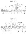
- the glass substrate 10 is subject to dicing process by use of a diamond cutter 31 to divide the glass substrate 10 into plural cover glasses 7, as shown in FIG. 11. Cooling water is poured from the nozzles 32 in order to prevent overheating of the diamond cutter 31 and the glass substrate 10. Since the adhesive 12 seals the gap between the spacer 6 and the wafer 26 in water-tight manner, the cooling water does not flow into the spacer 6 during the glass substrate dicing step S4.
- a dicing tape 34 is glued to the bottom surface of the wafer 26, as shown in FIG. 12.
- a diamond cutter 35 is actuated to dice the wafer 26 while pouring the cooling water from nozzles 36, and thereby, plural solid-state imaging devices 2 are manufactured.
- the adhesive 12 between the spacer 6 and the wafer 26 tightly keeps the cooling water from the nozzles 36 from flowing into the spacer 6.
- the transfer member is a flexible plastic film in the above embodiment, a rigid body with high flatness may be used as a transfer plate 38 for transferring the adhesive 39 to the spacer 6, as shown in FIG. 13A.
- the transfer plate 38 is, for instance, a glass plate. In the event of transferring the adhesive 39 by use of the transfer plate 38, it is necessary to release the transfer plate 38 slowly from the glass substrate 10 for the purpose of ensuring to transfer the adhesive 39 to the spacer 6.
- a release agent 37 such as silicon, may be coated on the surface of the transfer plate 38 for the purpose of increasing the peelability of the adhesive 39 from the transfer plate 38.
- any type of the adhesive 39 may be used if it is possible to apply the adhesive 39 to the release agent 37, and if the wettability of the adhesive 39 to the spacer 6 is better than that to the release agent 37.
- the adhesive 39 is applied to the release agent side of the transfer plate 39. Then, the transfer plate 38 is released from the glass substrate after sticking the transfer plate 38 to the spacer 6, as shown in FIG. 13B. The adhesive 39 on the release agent 37 is completely transferred to the spacer 6 over the area where the adhesive 39 comes in contact with the spacer 6.
- the thickness T3 of the adhesive 39 on the transfer plate 38 is the same as the thickness T4 of the adhesive 39 transferred to the spacer 6. Accordingly, the thickness of the adhesive 39 transferred to the spacer 6 is easily controlled by adjusting the thickness of the adhesive 39 applied on the transfer plate 38.
- the adhesive 39 with high viscosity is preferable.
- the release agent 37 is also applied to the transfer film 16 as the transfer member. It is also possible to provide a silicon coat film.
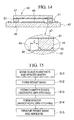
- the solid-state imaging device 40 may have a spacer 41 in which chamfer edges 43 are formed in the surface to be bonded to the solid-state imaging element chip 42 .
- the space between the chamfer edges 43 and the solid-state imaging element chip 42 can contain the surplus adhesive 44 to be flowed out, so it is possible to reduce the amount of the adhesive 44 to flow toward the solid-state imaging element 45. Accordingly, the surrounding area C between the spacer 41 and the solid-state imaging element 45 is reduced.
- the chamfered edges 43 may be formed according to the steps S11-S15 shown in FIG. 15.
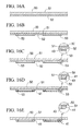
- an adhesive 51 is applied on a glass substrate 50 as the base material of the cover glass 47 (see FIG. 16A).
- the glass substrate 50 is bonded to a spacer wafer 52 as the base material of the spacer 41.
- a resist mask 53 is formed on the spacer wafer 52 (see FIG. 16B) .
- the resist mask 53 corresponds to the pattern of the spacers 41.
- the spacer wafer 52 is subject to isotropic dry etching to remove the spacer wafer 52 in the area that is not covered by the resist mask 53. Thereby, the chamfer edges 43 are formed underneath the resist mask 53, as shown in FIG. 16C.
- the spacer wafer 52 is subject to anisotropic dry etching to remove the spacer wafer 52 vertically, as shown in FIG. 16D.
- the resist mask 53 and the adhesive 51 are removed by ashing process to form the plural spacers 41 on the glass substrate 50 (see FIG. 16D).
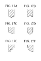
- the spacer may have other edge shapes.
- the edge shapes are convex, concave, taper, semi-circle, steps, and quarter circle, as shown in FIGS. 17A-17F.
- the spacers with these edge shapes can contain the surplus of the adhesive 12, and thus reduces the amount of the adhesive 12 to be flowed toward the solid-state imaging element 45.
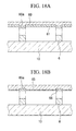
- a transfer member 60 may have a ridge pattern 60a that fits the spacers 6 formed in the glass substrate 10.
- An adhesive 61 is applied to the transfer member 60 with the ridge pattern 60a.
- a transfer member 65 may have recess pattern 65a that first the spacers 6, as shown in FIG. 18B.
- An adhesive 66 is applied to the transfer member 65 with the ridge pattern 65a. It is possible to adjust the amount of the adhesive 66 by controlling the depth of the recess pattern 65a.
- An elastic body like a flexible film and a rigid body like a glass plate may be used as the transfer member 60, 65.
- the CCD type solid-state imaging device is described in the above embodiment, a CMOS type solid-state imaging device is applied to the present invention.
- the present invention is also applicable to bonding a substrate to manufacture a chip with CSP structure other than the solid-state imaging device.
Landscapes
- Solid State Image Pick-Up Elements (AREA)
- Dicing (AREA)
- Transforming Light Signals Into Electric Signals (AREA)
- Facsimile Heads (AREA)
Applications Claiming Priority (4)
| Application Number | Priority Date | Filing Date | Title |
|---|---|---|---|
| JP2003083446 | 2003-03-25 | ||
| JP2003083446 | 2003-03-25 | ||
| JP2003320271 | 2003-09-11 | ||
| JP2003320271A JP2004312666A (ja) | 2003-03-25 | 2003-09-11 | 固体撮像装置及び固体撮像装置の製造方法 |
Publications (3)
| Publication Number | Publication Date |
|---|---|
| EP1463120A2 true EP1463120A2 (de) | 2004-09-29 |
| EP1463120A3 EP1463120A3 (de) | 2006-03-22 |
| EP1463120B1 EP1463120B1 (de) | 2008-07-23 |
Family
ID=32829038
Family Applications (1)
| Application Number | Title | Priority Date | Filing Date |
|---|---|---|---|
| EP04251592A Expired - Lifetime EP1463120B1 (de) | 2003-03-25 | 2004-03-19 | Verfahren zur Herstellung einer Festkörperbildaufnahmevorrichtung |
Country Status (5)
| Country | Link |
|---|---|
| US (3) | US7651881B2 (de) |
| EP (1) | EP1463120B1 (de) |
| JP (1) | JP2004312666A (de) |
| CN (1) | CN1294634C (de) |
| DE (1) | DE602004015181D1 (de) |
Cited By (6)
| Publication number | Priority date | Publication date | Assignee | Title |
|---|---|---|---|---|
| EP1503420A3 (de) * | 2003-08-01 | 2006-07-12 | Fuji Photo Film Co., Ltd. | Festkörperbildsensor und dessen Verfahren zur Herstellung |
| WO2007034929A1 (en) * | 2005-09-22 | 2007-03-29 | Fujifilm Corporation | Method for cutting solid-state image pickup device |
| WO2009006477A1 (en) * | 2007-07-02 | 2009-01-08 | Micron Technology, Inc. | Method of forming molded standoff structures on integrated circuit devices |
| EP1735829A4 (de) * | 2004-03-26 | 2009-03-04 | Fujifilm Corp | Einrichtung und verfahren zum verbinden von substraten |
| EP2264765A1 (de) * | 2009-06-19 | 2010-12-22 | Fraunhofer-Gesellschaft zur Förderung der angewandten Forschung e.V. | Gehäuse für eine Infrarot-Mikrovorrichtung und Verfahren zur Herstellung eines solchen Gehäuses |
| US12564308B2 (en) | 2021-04-19 | 2026-03-03 | Olympus Corporation | Image pickup unit, endoscope, and method for manufacturing image pickup unit |
Families Citing this family (30)
| Publication number | Priority date | Publication date | Assignee | Title |
|---|---|---|---|---|
| JP4510403B2 (ja) * | 2003-05-08 | 2010-07-21 | 富士フイルム株式会社 | カメラモジュール及びカメラモジュールの製造方法 |
| CN100470767C (zh) * | 2004-03-26 | 2009-03-18 | 富士胶片株式会社 | 接合衬底的装置及方法 |
| US7492023B2 (en) * | 2004-03-26 | 2009-02-17 | Fujifilm Corporation | Solid state imaging device |
| JP2006100763A (ja) * | 2004-09-06 | 2006-04-13 | Fuji Photo Film Co Ltd | 固体撮像装置の製造方法及び接合装置 |
| FR2879889B1 (fr) * | 2004-12-20 | 2007-01-26 | United Monolithic Semiconduct | Boitier miniature hyperfrequence et procede de fabrication du boitier |
| KR100922669B1 (ko) | 2005-01-04 | 2009-10-19 | 가부시키가이샤 아이스퀘어리서치 | 고체촬상장치 및 그 제조방법 |
| EP2573814B1 (de) | 2006-09-28 | 2015-03-11 | Fujifilm Corporation | Halbleiter-Bildsensor |
| JP5272300B2 (ja) * | 2006-11-14 | 2013-08-28 | 凸版印刷株式会社 | 固体撮像素子の製造方法 |
| WO2008072750A1 (en) * | 2006-12-11 | 2008-06-19 | Fujifilm Corporation | Solid-state image pickup device |
| JP5515223B2 (ja) * | 2008-02-12 | 2014-06-11 | ソニー株式会社 | 半導体装置 |
| JP5175620B2 (ja) * | 2008-05-29 | 2013-04-03 | シャープ株式会社 | 電子素子ウェハモジュールおよびその製造方法、電子素子モジュール、電子情報機器 |
| US20100083998A1 (en) * | 2008-10-06 | 2010-04-08 | Emcore Corporation | Solar Cell Receiver with a Glass Lid |
| US8125042B2 (en) * | 2008-11-13 | 2012-02-28 | Samsung Electronics Co., Ltd. | Semiconductor package and method of manufacturing the same |
| US8669633B2 (en) * | 2010-07-28 | 2014-03-11 | Teledyne Dalsa, Inc. | Packaged device with an image sensor aligned to a faceplate using fiducial marks and connection bodies registered thereto |
| JP2012039031A (ja) * | 2010-08-11 | 2012-02-23 | Nitto Denko Corp | 発光装置 |
| DE102010041576B4 (de) | 2010-09-29 | 2015-02-26 | Carl Zeiss Smt Gmbh | Verfahren zum Verbinden von Körpern, Verbundkörper sowie dessen Verwendung |
| US8912671B2 (en) * | 2013-05-16 | 2014-12-16 | Himax Technologies Limited | Semiconductor device having alignment mark |
| US9587425B2 (en) * | 2013-09-13 | 2017-03-07 | 3M Innovative Properties Company | Vacuum glazing pillars delivery films and methods for insulated glass units |
| US9346671B2 (en) * | 2014-02-04 | 2016-05-24 | Freescale Semiconductor, Inc. | Shielding MEMS structures during wafer dicing |
| US9419033B2 (en) * | 2014-10-24 | 2016-08-16 | Powertech Technology Inc. | Chip scale package of image sensor having dam combination |
| JP6701784B2 (ja) * | 2016-02-17 | 2020-05-27 | 株式会社リコー | 液体吐出ヘッド、液体吐出ユニット及び液体を吐出する装置 |
| US20170280034A1 (en) * | 2016-03-23 | 2017-09-28 | Magna Electronics Inc. | Vehicle vision system camera with enhanced imager and lens assembly |
| KR20190013917A (ko) * | 2016-05-30 | 2019-02-11 | 차이나 와퍼 레벨 씨에스피 씨오., 엘티디. | 패키징 구조체 및 패키징 방법 |
| US10032827B2 (en) * | 2016-06-29 | 2018-07-24 | Applied Materials, Inc. | Systems and methods for transfer of micro-devices |
| JP6791584B2 (ja) * | 2017-02-01 | 2020-11-25 | 株式会社ディスコ | 加工方法 |
| KR102048747B1 (ko) * | 2018-04-16 | 2019-11-26 | 한국기계연구원 | 마이크로 소자 전사방법 |
| KR102248527B1 (ko) * | 2019-05-02 | 2021-05-06 | 삼성전기주식회사 | 이미지 센서 패키지 |
| US11515347B2 (en) * | 2020-01-20 | 2022-11-29 | Omnivision Technologies, Inc. | Dam of image sensor module having sawtooth pattern and inclined surface on its inner wall and method of making same |
| TWI803990B (zh) * | 2021-09-24 | 2023-06-01 | 友達光電股份有限公司 | 移轉裝置與移轉方法 |
| JP2024148294A (ja) | 2023-04-05 | 2024-10-18 | キヤノン株式会社 | 電子モジュールおよび撮像装置 |
Family Cites Families (32)
| Publication number | Priority date | Publication date | Assignee | Title |
|---|---|---|---|---|
| JP2843464B2 (ja) * | 1992-09-01 | 1999-01-06 | シャープ株式会社 | 固体撮像装置 |
| US5896150A (en) * | 1992-11-25 | 1999-04-20 | Seiko Epson Corporation | Ink-jet type recording head |
| US6969635B2 (en) * | 2000-12-07 | 2005-11-29 | Reflectivity, Inc. | Methods for depositing, releasing and packaging micro-electromechanical devices on wafer substrates |
| US6114188A (en) * | 1996-04-12 | 2000-09-05 | Northeastern University | Method of fabricating an integrated complex-transition metal oxide device |
| US6027958A (en) * | 1996-07-11 | 2000-02-22 | Kopin Corporation | Transferred flexible integrated circuit |
| US6266872B1 (en) * | 1996-12-12 | 2001-07-31 | Tessera, Inc. | Method for making a connection component for a semiconductor chip package |
| US6531334B2 (en) * | 1997-07-10 | 2003-03-11 | Sony Corporation | Method for fabricating hollow package with a solid-state image device |
| JPH1131751A (ja) * | 1997-07-10 | 1999-02-02 | Sony Corp | 中空パッケージとその製造方法 |
| US5893726A (en) * | 1997-12-15 | 1999-04-13 | Micron Technology, Inc. | Semiconductor package with pre-fabricated cover and method of fabrication |
| US7091605B2 (en) * | 2001-09-21 | 2006-08-15 | Eastman Kodak Company | Highly moisture-sensitive electronic device element and method for fabrication |
| US6168965B1 (en) * | 1999-08-12 | 2001-01-02 | Tower Semiconductor Ltd. | Method for making backside illuminated image sensor |
| US6455774B1 (en) * | 1999-12-08 | 2002-09-24 | Amkor Technology, Inc. | Molded image sensor package |
| IL133453A0 (en) * | 1999-12-10 | 2001-04-30 | Shellcase Ltd | Methods for producing packaged integrated circuit devices and packaged integrated circuit devices produced thereby |
| JP2001185519A (ja) * | 1999-12-24 | 2001-07-06 | Hitachi Ltd | 半導体装置及びその製造方法 |
| US6285064B1 (en) * | 2000-03-28 | 2001-09-04 | Omnivision Technologies, Inc. | Chip scale packaging technique for optical image sensing integrated circuits |
| US6661084B1 (en) * | 2000-05-16 | 2003-12-09 | Sandia Corporation | Single level microelectronic device package with an integral window |
| JP2001351997A (ja) * | 2000-06-09 | 2001-12-21 | Canon Inc | 受光センサーの実装構造体およびその使用方法 |
| US6555417B2 (en) * | 2000-12-05 | 2003-04-29 | Analog Devices, Inc. | Method and device for protecting micro electromechanical system structures during dicing of a wafer |
| TW471143B (en) * | 2001-01-04 | 2002-01-01 | Wen-Wen Chiou | Integrated circuit chip package |
| JP2002231921A (ja) * | 2001-02-06 | 2002-08-16 | Olympus Optical Co Ltd | 固体撮像装置及びその製造方法 |
| JP2002289718A (ja) * | 2001-03-27 | 2002-10-04 | Kyocera Corp | 固体撮像装置 |
| JP4757398B2 (ja) * | 2001-04-24 | 2011-08-24 | Okiセミコンダクタ株式会社 | 半導体装置の製造方法 |
| EP2565924B1 (de) * | 2001-07-24 | 2018-01-10 | Samsung Electronics Co., Ltd. | Transferverfahren |
| JP3881888B2 (ja) * | 2001-12-27 | 2007-02-14 | セイコーエプソン株式会社 | 光デバイスの製造方法 |
| JP4095300B2 (ja) * | 2001-12-27 | 2008-06-04 | セイコーエプソン株式会社 | 光デバイス及びその製造方法、光モジュール、回路基板並びに電子機器 |
| JP4211256B2 (ja) * | 2001-12-28 | 2009-01-21 | セイコーエプソン株式会社 | 半導体集積回路、半導体集積回路の製造方法、電気光学装置、電子機器 |
| JP4443865B2 (ja) * | 2002-06-24 | 2010-03-31 | 富士フイルム株式会社 | 固体撮像装置およびその製造方法 |
| JP4037197B2 (ja) * | 2002-07-17 | 2008-01-23 | 富士フイルム株式会社 | 半導体撮像装置実装構造体の製造方法 |
| EP1686617A3 (de) * | 2002-07-29 | 2007-01-03 | Fuji Photo Film Co., Ltd. | Festkörper-Bildaufnehmer und Herstellungsverfahren dafür |
| US20040161871A1 (en) * | 2002-11-27 | 2004-08-19 | Seiko Epson Corporation | Semiconductor device, method of manufacturing the same, circuit substrate and electronic equipment |
| JP2004296453A (ja) * | 2003-02-06 | 2004-10-21 | Sharp Corp | 固体撮像装置、半導体ウエハ、光学装置用モジュール、固体撮像装置の製造方法及び光学装置用モジュールの製造方法 |
| TWI223428B (en) * | 2003-11-13 | 2004-11-01 | United Microelectronics Corp | Frame attaching process |
-
2003
- 2003-09-11 JP JP2003320271A patent/JP2004312666A/ja active Pending
-
2004
- 2004-03-19 DE DE602004015181T patent/DE602004015181D1/de not_active Expired - Lifetime
- 2004-03-19 EP EP04251592A patent/EP1463120B1/de not_active Expired - Lifetime
- 2004-03-23 CN CNB2004100315347A patent/CN1294634C/zh not_active Expired - Fee Related
- 2004-03-24 US US10/807,348 patent/US7651881B2/en not_active Expired - Fee Related
-
2005
- 2005-08-10 US US11/199,992 patent/US20060038204A1/en not_active Abandoned
-
2008
- 2008-05-29 US US12/128,739 patent/US20080231739A1/en not_active Abandoned
Cited By (11)
| Publication number | Priority date | Publication date | Assignee | Title |
|---|---|---|---|---|
| EP1503420A3 (de) * | 2003-08-01 | 2006-07-12 | Fuji Photo Film Co., Ltd. | Festkörperbildsensor und dessen Verfahren zur Herstellung |
| US7688382B2 (en) | 2003-08-01 | 2010-03-30 | Fujifilm Corporation | Solid-state imaging device and method for manufacturing the same |
| EP1735829A4 (de) * | 2004-03-26 | 2009-03-04 | Fujifilm Corp | Einrichtung und verfahren zum verbinden von substraten |
| WO2007034929A1 (en) * | 2005-09-22 | 2007-03-29 | Fujifilm Corporation | Method for cutting solid-state image pickup device |
| US7659147B2 (en) | 2005-09-22 | 2010-02-09 | Fujifilm Corporation | Method for cutting solid-state image pickup device |
| WO2009006477A1 (en) * | 2007-07-02 | 2009-01-08 | Micron Technology, Inc. | Method of forming molded standoff structures on integrated circuit devices |
| US7993977B2 (en) | 2007-07-02 | 2011-08-09 | Micron Technology, Inc. | Method of forming molded standoff structures on integrated circuit devices |
| EP2264765A1 (de) * | 2009-06-19 | 2010-12-22 | Fraunhofer-Gesellschaft zur Förderung der angewandten Forschung e.V. | Gehäuse für eine Infrarot-Mikrovorrichtung und Verfahren zur Herstellung eines solchen Gehäuses |
| WO2010146183A1 (en) * | 2009-06-19 | 2010-12-23 | Fraunhofer-Gesellschaft Zur Foerderung Der Angewandten Forschung E.V. | Housing for an infrared radiation micro device and method for fabricating such housing |
| US10002896B2 (en) | 2009-06-19 | 2018-06-19 | Fraunhofer-Gesellschaft Zur Foerderung Der Angewandten Forschung E.V. | Housing for an infrared radiation micro device and method for fabricating such housing |
| US12564308B2 (en) | 2021-04-19 | 2026-03-03 | Olympus Corporation | Image pickup unit, endoscope, and method for manufacturing image pickup unit |
Also Published As
| Publication number | Publication date |
|---|---|
| DE602004015181D1 (de) | 2008-09-04 |
| US20060038204A1 (en) | 2006-02-23 |
| US7651881B2 (en) | 2010-01-26 |
| EP1463120A3 (de) | 2006-03-22 |
| US20080231739A1 (en) | 2008-09-25 |
| US20040189855A1 (en) | 2004-09-30 |
| CN1294634C (zh) | 2007-01-10 |
| CN1542931A (zh) | 2004-11-03 |
| JP2004312666A (ja) | 2004-11-04 |
| EP1463120B1 (de) | 2008-07-23 |
Similar Documents
| Publication | Publication Date | Title |
|---|---|---|
| EP1463120B1 (de) | Verfahren zur Herstellung einer Festkörperbildaufnahmevorrichtung | |
| US6744109B2 (en) | Glass attachment over micro-lens arrays | |
| US7223626B2 (en) | Spacers for packaged microelectronic imagers and methods of making and using spacers for wafer-level packaging of imagers | |
| US8313971B2 (en) | Camera module manufacturing method and camera module | |
| CN101930105B (zh) | 光学元件模块、电子元件模块及其制造方法 | |
| US20060180887A1 (en) | Semiconductor device and production method thereof | |
| KR20060081202A (ko) | 보호판이 부착된 이미지 센서 칩과 그의 제조 방법 | |
| CN101752271A (zh) | 电子元件晶片模块、光学元件晶片模块及其制造方法 | |
| KR102333727B1 (ko) | 이미지 센서 모듈 및 이의 제조 방법 | |
| US7521657B2 (en) | Assembly having wafer with image sensor chips, a photo-sensitive adhesive pattern and plate thereof and method of manufacturing the same | |
| KR101317983B1 (ko) | 고체 촬상 장치를 절단하는 방법 | |
| TWI313057B (en) | Manufacturing method of semiconductor device | |
| US7037747B2 (en) | Method of manufacturing optical device | |
| EP2224272A1 (de) | Herstellungsverfahren und Struktur eines Moduls auf Waferebene | |
| US12062680B2 (en) | Solid-state imaging device, electronic apparatus, and method for producing solid-state imaging device | |
| JP2014168746A (ja) | 粘性材料の塗布装置、粘性材料の塗布方法、及び固体撮像装置の製造方法 | |
| US20120009394A1 (en) | Bonding method and bonding substrate | |
| JP2006080297A (ja) | 固体撮像装置及びその製造方法 | |
| TW201034060A (en) | Techniques for glass attachment in an image sensor package | |
| JPS5846187B2 (ja) | 固体撮像素子の製造方法 | |
| JP2010188252A (ja) | 樹脂材料の塗布方法およびマイクロレンズ基板の製造方法 | |
| JPS5864892A (ja) | カラ−固体撮像装置 |
Legal Events
| Date | Code | Title | Description |
|---|---|---|---|
| PUAI | Public reference made under article 153(3) epc to a published international application that has entered the european phase |
Free format text: ORIGINAL CODE: 0009012 |
|
| AK | Designated contracting states |
Kind code of ref document: A2 Designated state(s): AT BE BG CH CY CZ DE DK EE ES FI FR GB GR HU IE IT LI LU MC NL PL PT RO SE SI SK TR |
|
| AX | Request for extension of the european patent |
Extension state: AL HR LT LV MK |
|
| PUAL | Search report despatched |
Free format text: ORIGINAL CODE: 0009013 |
|
| AK | Designated contracting states |
Kind code of ref document: A3 Designated state(s): AT BE BG CH CY CZ DE DK EE ES FI FR GB GR HU IE IT LI LU MC NL PL PT RO SE SI SK TR |
|
| AX | Request for extension of the european patent |
Extension state: AL LT LV MK |
|
| 17P | Request for examination filed |
Effective date: 20060421 |
|
| AKX | Designation fees paid |
Designated state(s): DE FR GB |
|
| RAP1 | Party data changed (applicant data changed or rights of an application transferred) |
Owner name: FUJIFILM CORPORATION |
|
| 17Q | First examination report despatched |
Effective date: 20070718 |
|
| GRAP | Despatch of communication of intention to grant a patent |
Free format text: ORIGINAL CODE: EPIDOSNIGR1 |
|
| RTI1 | Title (correction) |
Free format text: METHOD OF MANUFACTURING A SOLID-STATE IMAGING DEVICE |
|
| GRAS | Grant fee paid |
Free format text: ORIGINAL CODE: EPIDOSNIGR3 |
|
| GRAA | (expected) grant |
Free format text: ORIGINAL CODE: 0009210 |
|
| AK | Designated contracting states |
Kind code of ref document: B1 Designated state(s): DE FR GB |
|
| REG | Reference to a national code |
Ref country code: GB Ref legal event code: FG4D |
|
| REF | Corresponds to: |
Ref document number: 602004015181 Country of ref document: DE Date of ref document: 20080904 Kind code of ref document: P |
|
| PLBE | No opposition filed within time limit |
Free format text: ORIGINAL CODE: 0009261 |
|
| STAA | Information on the status of an ep patent application or granted ep patent |
Free format text: STATUS: NO OPPOSITION FILED WITHIN TIME LIMIT |
|
| 26N | No opposition filed |
Effective date: 20090424 |
|
| PGFP | Annual fee paid to national office [announced via postgrant information from national office to epo] |
Ref country code: FR Payment date: 20140311 Year of fee payment: 11 |
|
| PGFP | Annual fee paid to national office [announced via postgrant information from national office to epo] |
Ref country code: GB Payment date: 20140319 Year of fee payment: 11 |
|
| PGFP | Annual fee paid to national office [announced via postgrant information from national office to epo] |
Ref country code: DE Payment date: 20140417 Year of fee payment: 11 |
|
| REG | Reference to a national code |
Ref country code: DE Ref legal event code: R119 Ref document number: 602004015181 Country of ref document: DE |
|
| GBPC | Gb: european patent ceased through non-payment of renewal fee |
Effective date: 20150319 |
|
| REG | Reference to a national code |
Ref country code: FR Ref legal event code: ST Effective date: 20151130 |
|
| PG25 | Lapsed in a contracting state [announced via postgrant information from national office to epo] |
Ref country code: GB Free format text: LAPSE BECAUSE OF NON-PAYMENT OF DUE FEES Effective date: 20150319 Ref country code: DE Free format text: LAPSE BECAUSE OF NON-PAYMENT OF DUE FEES Effective date: 20151001 |
|
| PG25 | Lapsed in a contracting state [announced via postgrant information from national office to epo] |
Ref country code: FR Free format text: LAPSE BECAUSE OF NON-PAYMENT OF DUE FEES Effective date: 20150331 |