EP2224272A1 - Herstellungsverfahren und Struktur eines Moduls auf Waferebene - Google Patents
Herstellungsverfahren und Struktur eines Moduls auf Waferebene Download PDFInfo
- Publication number
- EP2224272A1 EP2224272A1 EP10152636A EP10152636A EP2224272A1 EP 2224272 A1 EP2224272 A1 EP 2224272A1 EP 10152636 A EP10152636 A EP 10152636A EP 10152636 A EP10152636 A EP 10152636A EP 2224272 A1 EP2224272 A1 EP 2224272A1
- Authority
- EP
- European Patent Office
- Prior art keywords
- adhesive film
- solid adhesive
- substrate
- wafer level
- film
- Prior art date
- Legal status (The legal status is an assumption and is not a legal conclusion. Google has not performed a legal analysis and makes no representation as to the accuracy of the status listed.)
- Granted
Links
Images

Classifications
-
- G—PHYSICS
- G02—OPTICS
- G02B—OPTICAL ELEMENTS, SYSTEMS OR APPARATUS
- G02B3/00—Simple or compound lenses
- G02B3/0006—Arrays
- G02B3/0012—Arrays characterised by the manufacturing method
-
- G—PHYSICS
- G02—OPTICS
- G02B—OPTICAL ELEMENTS, SYSTEMS OR APPARATUS
- G02B13/00—Optical objectives specially designed for the purposes specified below
- G02B13/001—Miniaturised objectives for electronic devices, e.g. portable telephones, webcams, PDAs, small digital cameras
- G02B13/0085—Miniaturised objectives for electronic devices, e.g. portable telephones, webcams, PDAs, small digital cameras employing wafer level optics
-
- G—PHYSICS
- G02—OPTICS
- G02B—OPTICAL ELEMENTS, SYSTEMS OR APPARATUS
- G02B7/00—Mountings, adjusting means, or light-tight connections, for optical elements
- G02B7/02—Mountings, adjusting means, or light-tight connections, for optical elements for lenses
- G02B7/025—Mountings, adjusting means, or light-tight connections, for optical elements for lenses using glue
-
- G—PHYSICS
- G02—OPTICS
- G02B—OPTICAL ELEMENTS, SYSTEMS OR APPARATUS
- G02B13/00—Optical objectives specially designed for the purposes specified below
- G02B13/001—Miniaturised objectives for electronic devices, e.g. portable telephones, webcams, PDAs, small digital cameras
-
- Y—GENERAL TAGGING OF NEW TECHNOLOGICAL DEVELOPMENTS; GENERAL TAGGING OF CROSS-SECTIONAL TECHNOLOGIES SPANNING OVER SEVERAL SECTIONS OF THE IPC; TECHNICAL SUBJECTS COVERED BY FORMER USPC CROSS-REFERENCE ART COLLECTIONS [XRACs] AND DIGESTS
- Y10—TECHNICAL SUBJECTS COVERED BY FORMER USPC
- Y10T—TECHNICAL SUBJECTS COVERED BY FORMER US CLASSIFICATION
- Y10T428/00—Stock material or miscellaneous articles
- Y10T428/14—Layer or component removable to expose adhesive
- Y10T428/1471—Protective layer
-
- Y—GENERAL TAGGING OF NEW TECHNOLOGICAL DEVELOPMENTS; GENERAL TAGGING OF CROSS-SECTIONAL TECHNOLOGIES SPANNING OVER SEVERAL SECTIONS OF THE IPC; TECHNICAL SUBJECTS COVERED BY FORMER USPC CROSS-REFERENCE ART COLLECTIONS [XRACs] AND DIGESTS
- Y10—TECHNICAL SUBJECTS COVERED BY FORMER USPC
- Y10T—TECHNICAL SUBJECTS COVERED BY FORMER US CLASSIFICATION
- Y10T428/00—Stock material or miscellaneous articles
- Y10T428/14—Layer or component removable to expose adhesive
- Y10T428/1476—Release layer
Definitions
- the present invention generally relates to a wafer level module, and more particularly to a structure and fabricating method of a wafer level module with a solid adhesive film.
- Wafer level optics is a technique of fabricating miniaturized optics such as lens module or camera module at the wafer level using semiconductor techniques.
- the wafer level optics is well adapted to mobile or handheld devices.
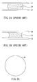
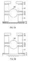
- liquid adhesive is usually applied, for example, by screen printing or coating, between two substrates that are to be bonded. Owing to the characteristics of the liquid adhesive, the thickness of the resultant adhesive layer could not be maintained constant. Further, the liquid adhesive 10 may result in overflow between two substrates 12 and 14 as shown in Fig. 1A or Fig. 1B . In the worst case, the shift of the liquid adhesive may cause misalignment between the substrates, thereby malfunctioning the resultant module. Accordingly, the patterns of the module are commonly designed with larger margin, and thus fewer modules may be fabricated on a wafer. Moreover, substantive portion of time is consumed in coating or printing the liquid adhesive, particularly to a module with complex patterns.
- a wafer level lens module or camera module normally requires using additional adjustment means, such as a screw, in order to mechanically arrive at a required focus.
- additional adjustment means such as a screw
- a first solid adhesive film with a first release film and a second release film that respectively cover a first surface and a second surface of the first solid adhesive film is firstly provided. Openings are then patterned through the first solid adhesive film. After removing the first release films to expose the first surface of the first solid adhesive film, the exposed first surface of the first solid adhesive film is aligned and adhered to a first substrate. After removing the second release film to expose the second surface of the first solid adhesive film, the exposed second surface of the first solid adhesive film is aligned and adhered to a second substrate, thereby resulting in a wafer level module.
- the first substrate comprises a first spacer layer and the second substrate comprises a lens substrate
- a third substrate is further aligned and adhered to the second substrate via a patterned second solid adhesive film
- a diaphragm layer is aligned and adhered to the third substrate via a patterned third solid adhesive film.
- a fourth solid adhesive film is aligned and adhered to the first substrate with one removable release film covering the fourth solid adhesive film. Slicing is performed to result in a number of wafer level lens modules with the removable release film.
- the release film is removed to expose the fourth solid adhesive film, and the exposed fourth solid adhesive film is aligned and adhered to an image sensor.
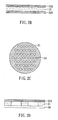
- Fig. 2A to Fig. 2F illustrate a structure and fabricating method of a wafer level module according to a first embodiment of the present invention.
- a (transparent) solid adhesive film (or solid glue film) 21 is firstly provided as shown in Fig. 2A (a top view) and Fig. 2B (a cross-sectional view).
- the solid adhesive film 21 is normally accompanied with a first release (or protective) film 22A and a second release film 22B that respectively cover a top surface and a bottom surface of the solid adhesive film 21.
- the first/second release films 22A/B are used to shield the solid adhesive film 21 before applying the solid adhesive film 21.
- the solid adhesive film 21, in the embodiment, is primarily made of thermosetting material such as, but not limited to, epoxy, which is pre-cured into solid form as an adhesive.
- the solid adhesive film 21 covered with the first/second release films 22A/B are then subjected to patterning to result in plural openings (or holes) 23 passing through the solid adhesive film 21 and the first/second release film 22A/B as shown in Fig. 2C .
- the openings 23 may be designed to any shape (e.g., circle, rectangle, polygon or other shape) and size.
- the openings 23 may be patterned by physical means (such as hole punching or laser cutting) or chemical means (such as exposure and then etch).
- one of the release films e.g., the second release film 22B
- one of the release films is peeled or stripped off to expose one surface (e.g., the bottom surface) of the solid adhesive film 21.
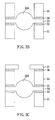
- the exposed surface of the solid adhesive film 21 is then aligned and adhered (or bonded) to a first substrate 24 as shown in Fig. 2D .
- the first substrate 24 may, for example, be a semiconductor wafer, a glass substrate, lens substrate or any substrate suitable for wafer level fabrication.
- the resultant product shown in Fig. 2D may be shipped or sold as a half-finished (or intermediate) product that may be further processed (by others) to result in a finished product.
- the other release film e.g., the first release film 22A
- the other release film is also peeled or stripped off to expose the other surface (e.g., the top surface) of the solid adhesive film 21, resulting in a structure shown in Fig. 2E .
- the exposed surface of the solid adhesive film 21 is then aligned and adhered (or bonded) to a second substrate 25 as shown in Fig. 2F .
- heat or/and pressure is commonly applied. The amount of the heat and the pressure varies according to specific application. For example, the structure of Fig.
- the second substrate 25 may, for example, be a semiconductor wafer, a glass substrate, lens substrate or any substrate suitable for wafer level fabrication. It is noted that the first substrate 24 and the second substrate 25 may not necessarily contain the same material.
- the first substrate 24 may be a semiconductor (e.g., sapphire) substrate and the second substrate 25 may be a glass substrate with lens.
- the first substrate 24 may be a semiconductor (e.g., sapphire) substrate and the second substrate 25 may be a glass substrate with lens.
- the thickness of the resultant adhesive layer (i.e., the solid adhesive film 21) between the first substrate 24 and the second substrate 25 may be substantially maintained constant compared to the conventional counterpart that uses liquid adhesive.
- the dimension of the pattern in the adhesive layer (i.e., the solid adhesive film 21) may be precisely controlled with less margin, and, therefore, more (or denser) patterns may be fabricated on a wafer, thereby increasing yield and cost efficiency.
- the adhesive layer (i.e., the solid adhesive film 21) in the embodiment is pre-patterned rather than is coated (e.g., screen printed) as in the conventional process, substantive time may thus be saved and patterns with more complex shape may be attainable.
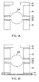
- Fig. 3A to Fig. 3C illustrate a structure and fabricating method of a wafer level lens module according to a second embodiment of the present invention. It is appreciated by those skilled in the art that the order of performing the fabrication may be different from or even opposite to that shown in Figs. 3A-3C .
- a first substrate 31 is firstly adhered (or bonded) to a second substrate 33 via a (patterned) first solid adhesive film 32.
- the fist substrate 31 is a first (patterned) spacer layer and the second substrate 33 is a lens substrate.
- the bonding between the first spacer layer 31 and the lens substrate 33, and the patterning of the first solid adhesive film 32 have been described in the first embodiment and are thus omitted here for brevity.
- the second substrate (e.g., the lens substrate) 33 is adhered to a third substrate (e.g., a second spacer layer) 35 via a (patterned) second solid adhesive film 34.
- a third substrate e.g., a second spacer layer
- the first and second solid adhesive films 32 and 34 have patterns (such as circular openings) with dimension that approximates that of the lens 330 of the lens substrate 33.
- a diaphragm layer 37 is adhered to the third substrate (i.e., the second spacer layer) 35 via a (patterned) third solid adhesive film 36.
- the diaphragm layer 37 is used as an iris of a camera, and is made of a solid adhesive film that is dyed beforehand for blocking light. After subjecting the entire wafer to slicing, the individual wafer level lens module as shown in Fig. 3C may therefore be obtained.
- the first/ second/ third solid adhesive films 32/34/36 provide the same advantages of the first embodiment. Furthermore, the thickness of the first/second/third solid adhesive films 32/34/36 in the present embodiment may be properly pre-selected such that the focus of the resultant lens module may be precisely pre-determined without resorting to the adjustment using screw as in the conventional art.
- Fig. 4A to Fig. 4B illustrate a structure and fabricating method of a wafer level lens module according to a third embodiment of the present invention.
- a wafer level lens module such as that of Fig. 3C before slicing is provided. Same numerals as those in the previous embodiment are therefore used in the present embodiment. For brevity, only one module has been illustrated in the figure.
- a fourth solid adhesive film 41 is aligned and adhered to the bottom surface of the first substrate (i.e., the first spacer layer) 31. It is observed in the figure that one release film 42 remains covering the bottom surface of the fourth solid adhesive film 41.
- the individual wafer level lens module as shown in Fig. 4B may therefore be obtained.
- the resultant product shown in Fig. 4B may be shipped or sold as a half-finished (or intermediate) product that may be further processed (by others) to result in a finished product.
- a person receiving this half-finished product may peel off the release film 42 to expose the bottom surface of the fourth solid adhesive film 41, followed by adhering the exposed surface, for example, to an image sensor (not shown), thereby resulting in a wafer level camera module.
- Fig. 5A to Fig. 5B illustrate a structure and fabricating method of a (wafer level) compact camera module (CCM) according to a fourth embodiment of the present invention.
- a wafer level lens module such as that of Fig. 4B is provided.
- the module may be either non-sliced or sliced. Same numerals as those in the previous embodiment are therefore used in the present embodiment.
- the release film 42 covering the fourth solid adhesive film 41 is peeled off, followed by aligning and adhering the lens module to an image sensor 51 such as a complementary metal oxide semiconductor (CMOS) image sensor or a charge coupled device (CCD).
- CMOS complementary metal oxide semiconductor
- CCD charge coupled device
- the fourth solid adhesive film 41 may not overflow or shift even under pressure, and the image sensor 51 therefore will not be abnormally blocked by overflowing liquid glue as occurred in the conventional art.
Landscapes
- Physics & Mathematics (AREA)
- General Physics & Mathematics (AREA)
- Optics & Photonics (AREA)
- Engineering & Computer Science (AREA)
- Manufacturing & Machinery (AREA)
- Solid State Image Pick-Up Elements (AREA)
- Lens Barrels (AREA)
- Dicing (AREA)
Applications Claiming Priority (2)
| Application Number | Priority Date | Filing Date | Title |
|---|---|---|---|
| US23918409P | 2009-09-02 | 2009-09-02 | |
| US12/646,094 US8193599B2 (en) | 2009-09-02 | 2009-12-23 | Fabricating method and structure of a wafer level module |
Publications (2)
| Publication Number | Publication Date |
|---|---|
| EP2224272A1 true EP2224272A1 (de) | 2010-09-01 |
| EP2224272B1 EP2224272B1 (de) | 2011-10-26 |
Family
ID=42062610
Family Applications (1)
| Application Number | Title | Priority Date | Filing Date |
|---|---|---|---|
| EP10152636A Not-in-force EP2224272B1 (de) | 2009-09-02 | 2010-02-04 | Herstellungsverfahren und Struktur eines Moduls auf Waferebene |
Country Status (5)
| Country | Link |
|---|---|
| US (1) | US8193599B2 (de) |
| EP (1) | EP2224272B1 (de) |
| JP (1) | JP2011053640A (de) |
| KR (1) | KR101124652B1 (de) |
| AT (1) | ATE530940T1 (de) |
Cited By (1)
| Publication number | Priority date | Publication date | Assignee | Title |
|---|---|---|---|---|
| CN102654629A (zh) * | 2011-03-01 | 2012-09-05 | 英属盖曼群岛恒景科技股份有限公司 | 镜头模块与制造镜头模块的光圈的方法 |
Families Citing this family (5)
| Publication number | Priority date | Publication date | Assignee | Title |
|---|---|---|---|---|
| CN102045494A (zh) * | 2009-10-22 | 2011-05-04 | 国碁电子(中山)有限公司 | 相机模组及其制作方法 |
| SG2014008726A (en) * | 2011-08-25 | 2014-04-28 | Heptagon Micro Optics Pte Ltd | Wafer-level fabrication of optical devices with front focal length correction |
| US8388793B1 (en) * | 2011-08-29 | 2013-03-05 | Visera Technologies Company Limited | Method for fabricating camera module |
| AU2015308583B2 (en) | 2014-08-29 | 2019-11-28 | Medical Components, Inc. | Huber safety needle |
| JP6896753B2 (ja) | 2016-03-18 | 2021-06-30 | メデイカル コンポーネンツ,インコーポレーテツド | フーバー針アセンブリ |
Citations (6)
| Publication number | Priority date | Publication date | Assignee | Title |
|---|---|---|---|---|
| US6537854B1 (en) * | 1999-05-24 | 2003-03-25 | Industrial Technology Research Institute | Method for bonding IC chips having multi-layered bumps with corrugated surfaces and devices formed |
| US20050254133A1 (en) * | 2004-05-13 | 2005-11-17 | Salman Akram | Integrated optics units and methods of manufacturing integrated optics units for use with microelectronic imagers |
| EP1674910A1 (de) * | 2004-12-27 | 2006-06-28 | Canon Kabushiki Kaisha | Verfahren zur Befestigung eines optischen Elements und auf diese Weise hergestellte optische Einheit |
| EP1811772A2 (de) * | 2006-01-24 | 2007-07-25 | Visera Technologies Company Ltd. | Bildsensormodul mit präziser Bildprojektionssteuerung |
| US20070217019A1 (en) * | 2006-03-16 | 2007-09-20 | Wen-Kuei Huang | Optical components array device, microlens array and process of fabricating thereof |
| US20090206431A1 (en) | 2008-02-20 | 2009-08-20 | Micron Technology, Inc. | Imager wafer level module and method of fabrication and use |
Family Cites Families (17)
| Publication number | Priority date | Publication date | Assignee | Title |
|---|---|---|---|---|
| JPS61110396A (ja) * | 1984-11-05 | 1986-05-28 | Fujitsu Ltd | 半導体記憶装置 |
| JPH09111204A (ja) | 1995-10-16 | 1997-04-28 | Shinko Electric Ind Co Ltd | 導電性接着テープおよびこれを用いた半導体装置用パッケージ |
| JP2000007758A (ja) * | 1998-06-27 | 2000-01-11 | Nagase Chiba Kk | B−ステージ化できる液状エポキシ樹脂組成物 |
| US6428641B1 (en) * | 1998-08-31 | 2002-08-06 | Amkor Technology, Inc. | Method for laminating circuit pattern tape on semiconductor wafer |
| US6591125B1 (en) * | 2000-06-27 | 2003-07-08 | Therasense, Inc. | Small volume in vitro analyte sensor with diffusible or non-leachable redox mediator |
| JP2000332414A (ja) * | 1999-05-20 | 2000-11-30 | Nec Corp | 樹脂付き配線シート、それを用いた配線構造とそれらの製造方法 |
| JP2001245217A (ja) * | 2000-03-02 | 2001-09-07 | Olympus Optical Co Ltd | 小型撮像モジュール |
| US6707163B2 (en) * | 2001-04-13 | 2004-03-16 | Stmicroelectronics, Inc. | Method of eliminating uncontrolled voids in sheet adhesive layer |
| JP2004200965A (ja) | 2002-12-18 | 2004-07-15 | Sanyo Electric Co Ltd | カメラモジュール及びその製造方法 |
| US7135352B2 (en) * | 2004-02-26 | 2006-11-14 | Eastman Kodak Company | Method of fabricating a cover plate bonded over an encapsulated OLEDs |
| US7863702B2 (en) * | 2004-06-10 | 2011-01-04 | Samsung Electronics Co., Ltd. | Image sensor package and method of manufacturing the same |
| JP3801601B2 (ja) | 2004-06-15 | 2006-07-26 | シャープ株式会社 | 蓋部を備えた半導体ウェハの製造方法及び半導体装置の製造方法 |
| US7964926B2 (en) * | 2005-02-02 | 2011-06-21 | Samsung Electronics Co., Ltd. | Image sensing devices including image sensor chips, image sensor package modules employing the image sensing devices, electronic products employing the image sensor package modules, and methods of fabricating the same |
| JP4304163B2 (ja) * | 2005-03-09 | 2009-07-29 | パナソニック株式会社 | 撮像モジュールおよびその製造方法 |
| WO2007059152A1 (en) * | 2005-11-14 | 2007-05-24 | World Properties, Inc. | Circuit material, multi-layer circuits, and methods of manufacture thereof |
| US7833577B2 (en) * | 2007-05-11 | 2010-11-16 | 3M Innovative Properties Company | Methods of making a pressure-sensitive adhesive assembly |
| US8361830B2 (en) * | 2010-04-09 | 2013-01-29 | Himax Semiconductor, Inc. | Image sensor module and method of manufacturing the same |
-
2009
- 2009-12-23 US US12/646,094 patent/US8193599B2/en not_active Expired - Fee Related
-
2010
- 2010-02-03 JP JP2010022189A patent/JP2011053640A/ja active Pending
- 2010-02-04 EP EP10152636A patent/EP2224272B1/de not_active Not-in-force
- 2010-02-04 AT AT10152636T patent/ATE530940T1/de not_active IP Right Cessation
- 2010-03-03 KR KR1020100019008A patent/KR101124652B1/ko not_active Expired - Fee Related
Patent Citations (6)
| Publication number | Priority date | Publication date | Assignee | Title |
|---|---|---|---|---|
| US6537854B1 (en) * | 1999-05-24 | 2003-03-25 | Industrial Technology Research Institute | Method for bonding IC chips having multi-layered bumps with corrugated surfaces and devices formed |
| US20050254133A1 (en) * | 2004-05-13 | 2005-11-17 | Salman Akram | Integrated optics units and methods of manufacturing integrated optics units for use with microelectronic imagers |
| EP1674910A1 (de) * | 2004-12-27 | 2006-06-28 | Canon Kabushiki Kaisha | Verfahren zur Befestigung eines optischen Elements und auf diese Weise hergestellte optische Einheit |
| EP1811772A2 (de) * | 2006-01-24 | 2007-07-25 | Visera Technologies Company Ltd. | Bildsensormodul mit präziser Bildprojektionssteuerung |
| US20070217019A1 (en) * | 2006-03-16 | 2007-09-20 | Wen-Kuei Huang | Optical components array device, microlens array and process of fabricating thereof |
| US20090206431A1 (en) | 2008-02-20 | 2009-08-20 | Micron Technology, Inc. | Imager wafer level module and method of fabrication and use |
Cited By (1)
| Publication number | Priority date | Publication date | Assignee | Title |
|---|---|---|---|---|
| CN102654629A (zh) * | 2011-03-01 | 2012-09-05 | 英属盖曼群岛恒景科技股份有限公司 | 镜头模块与制造镜头模块的光圈的方法 |
Also Published As
| Publication number | Publication date |
|---|---|
| JP2011053640A (ja) | 2011-03-17 |
| US20110049547A1 (en) | 2011-03-03 |
| KR101124652B1 (ko) | 2012-03-20 |
| ATE530940T1 (de) | 2011-11-15 |
| EP2224272B1 (de) | 2011-10-26 |
| US8193599B2 (en) | 2012-06-05 |
| KR20110025037A (ko) | 2011-03-09 |
Similar Documents
| Publication | Publication Date | Title |
|---|---|---|
| TWI411024B (zh) | 晶圓級模組及其製造方法 | |
| CN101930105B (zh) | 光学元件模块、电子元件模块及其制造方法 | |
| US10199426B2 (en) | Optoelectronic modules that have shielding to reduce light leakage or stray light, and fabrication methods for such modules | |
| EP2224272B1 (de) | Herstellungsverfahren und Struktur eines Moduls auf Waferebene | |
| US7223626B2 (en) | Spacers for packaged microelectronic imagers and methods of making and using spacers for wafer-level packaging of imagers | |
| US7378724B2 (en) | Cavity structure for semiconductor structures | |
| CN1294634C (zh) | 固态成像装置及其制造方法 | |
| US9525002B2 (en) | Image sensor device with sensing surface cavity and related methods | |
| TWI647824B (zh) | 製造被動光學元件的方法及包含該元件的裝置 | |
| US8388793B1 (en) | Method for fabricating camera module | |
| JP2003197885A (ja) | 光デバイス及びその製造方法、光モジュール、回路基板並びに電子機器 | |
| WO2014007758A1 (en) | Use of vacuum chucks to hold a wafer or wafer sub-stack | |
| CN105489620A (zh) | 固体摄像装置的制造方法以及摄像机模块的制造方法 | |
| CN107425030B (zh) | 光学晶片的制造 | |
| US9013017B2 (en) | Method for making image sensors using wafer-level processing and associated devices | |
| JP2006100762A (ja) | 固体撮像装置の製造方法 | |
| JP2010021267A (ja) | 積層部品、画像取得装置、及び生体情報取得装置 | |
| EP4498416A1 (de) | Verfahren zur übertragung von chips, träger zur übertragung geladener chips und verwendung davon | |
| TW202537058A (zh) | 半導體裝置、及半導體裝置之製造方法 | |
| WO2020256635A1 (en) | Replicating optical elements onto a substrate | |
| HK1211743A1 (en) | Wafer-level bonding method for camera fabrication | |
| HK1211743B (en) | Wafer-level bonding method for camera fabrication | |
| JP2007329352A (ja) | 固体撮像素子モジュールの製造方法 |
Legal Events
| Date | Code | Title | Description |
|---|---|---|---|
| PUAI | Public reference made under article 153(3) epc to a published international application that has entered the european phase |
Free format text: ORIGINAL CODE: 0009012 |
|
| 17P | Request for examination filed |
Effective date: 20100204 |
|
| AK | Designated contracting states |
Kind code of ref document: A1 Designated state(s): AT BE BG CH CY CZ DE DK EE ES FI FR GB GR HR HU IE IS IT LI LT LU LV MC MK MT NL NO PL PT RO SE SI SK SM TR |
|
| AX | Request for extension of the european patent |
Extension state: AL BA RS |
|
| 17Q | First examination report despatched |
Effective date: 20101026 |
|
| RIC1 | Information provided on ipc code assigned before grant |
Ipc: G02B 7/02 20060101AFI20110322BHEP |
|
| GRAP | Despatch of communication of intention to grant a patent |
Free format text: ORIGINAL CODE: EPIDOSNIGR1 |
|
| RAP1 | Party data changed (applicant data changed or rights of an application transferred) |
Owner name: HIMAX SEMICONDUCTOR, INC. |
|
| GRAS | Grant fee paid |
Free format text: ORIGINAL CODE: EPIDOSNIGR3 |
|
| GRAA | (expected) grant |
Free format text: ORIGINAL CODE: 0009210 |
|
| AK | Designated contracting states |
Kind code of ref document: B1 Designated state(s): AT BE BG CH CY CZ DE DK EE ES FI FR GB GR HR HU IE IS IT LI LT LU LV MC MK MT NL NO PL PT RO SE SI SK SM TR |
|
| REG | Reference to a national code |
Ref country code: GB Ref legal event code: FG4D |
|
| REG | Reference to a national code |
Ref country code: CH Ref legal event code: EP |
|
| REG | Reference to a national code |
Ref country code: IE Ref legal event code: FG4D |
|
| REG | Reference to a national code |
Ref country code: DE Ref legal event code: R096 Ref document number: 602010000297 Country of ref document: DE Effective date: 20111229 |
|
| REG | Reference to a national code |
Ref country code: NL Ref legal event code: T3 |
|
| LTIE | Lt: invalidation of european patent or patent extension |
Effective date: 20111026 |
|
| REG | Reference to a national code |
Ref country code: AT Ref legal event code: MK05 Ref document number: 530940 Country of ref document: AT Kind code of ref document: T Effective date: 20111026 |
|
| PG25 | Lapsed in a contracting state [announced via postgrant information from national office to epo] |
Ref country code: IS Free format text: LAPSE BECAUSE OF FAILURE TO SUBMIT A TRANSLATION OF THE DESCRIPTION OR TO PAY THE FEE WITHIN THE PRESCRIBED TIME-LIMIT Effective date: 20120226 Ref country code: LT Free format text: LAPSE BECAUSE OF FAILURE TO SUBMIT A TRANSLATION OF THE DESCRIPTION OR TO PAY THE FEE WITHIN THE PRESCRIBED TIME-LIMIT Effective date: 20111026 Ref country code: NO Free format text: LAPSE BECAUSE OF FAILURE TO SUBMIT A TRANSLATION OF THE DESCRIPTION OR TO PAY THE FEE WITHIN THE PRESCRIBED TIME-LIMIT Effective date: 20120126 Ref country code: BE Free format text: LAPSE BECAUSE OF FAILURE TO SUBMIT A TRANSLATION OF THE DESCRIPTION OR TO PAY THE FEE WITHIN THE PRESCRIBED TIME-LIMIT Effective date: 20111026 |
|
| PG25 | Lapsed in a contracting state [announced via postgrant information from national office to epo] |
Ref country code: LV Free format text: LAPSE BECAUSE OF FAILURE TO SUBMIT A TRANSLATION OF THE DESCRIPTION OR TO PAY THE FEE WITHIN THE PRESCRIBED TIME-LIMIT Effective date: 20111026 Ref country code: GR Free format text: LAPSE BECAUSE OF FAILURE TO SUBMIT A TRANSLATION OF THE DESCRIPTION OR TO PAY THE FEE WITHIN THE PRESCRIBED TIME-LIMIT Effective date: 20120127 Ref country code: SE Free format text: LAPSE BECAUSE OF FAILURE TO SUBMIT A TRANSLATION OF THE DESCRIPTION OR TO PAY THE FEE WITHIN THE PRESCRIBED TIME-LIMIT Effective date: 20111026 Ref country code: PL Free format text: LAPSE BECAUSE OF FAILURE TO SUBMIT A TRANSLATION OF THE DESCRIPTION OR TO PAY THE FEE WITHIN THE PRESCRIBED TIME-LIMIT Effective date: 20111026 Ref country code: HR Free format text: LAPSE BECAUSE OF FAILURE TO SUBMIT A TRANSLATION OF THE DESCRIPTION OR TO PAY THE FEE WITHIN THE PRESCRIBED TIME-LIMIT Effective date: 20111026 Ref country code: PT Free format text: LAPSE BECAUSE OF FAILURE TO SUBMIT A TRANSLATION OF THE DESCRIPTION OR TO PAY THE FEE WITHIN THE PRESCRIBED TIME-LIMIT Effective date: 20120227 Ref country code: SI Free format text: LAPSE BECAUSE OF FAILURE TO SUBMIT A TRANSLATION OF THE DESCRIPTION OR TO PAY THE FEE WITHIN THE PRESCRIBED TIME-LIMIT Effective date: 20111026 |
|
| PG25 | Lapsed in a contracting state [announced via postgrant information from national office to epo] |
Ref country code: CY Free format text: LAPSE BECAUSE OF FAILURE TO SUBMIT A TRANSLATION OF THE DESCRIPTION OR TO PAY THE FEE WITHIN THE PRESCRIBED TIME-LIMIT Effective date: 20111026 |
|
| PG25 | Lapsed in a contracting state [announced via postgrant information from national office to epo] |
Ref country code: DK Free format text: LAPSE BECAUSE OF FAILURE TO SUBMIT A TRANSLATION OF THE DESCRIPTION OR TO PAY THE FEE WITHIN THE PRESCRIBED TIME-LIMIT Effective date: 20111026 Ref country code: CZ Free format text: LAPSE BECAUSE OF FAILURE TO SUBMIT A TRANSLATION OF THE DESCRIPTION OR TO PAY THE FEE WITHIN THE PRESCRIBED TIME-LIMIT Effective date: 20111026 Ref country code: BG Free format text: LAPSE BECAUSE OF FAILURE TO SUBMIT A TRANSLATION OF THE DESCRIPTION OR TO PAY THE FEE WITHIN THE PRESCRIBED TIME-LIMIT Effective date: 20120126 Ref country code: SK Free format text: LAPSE BECAUSE OF FAILURE TO SUBMIT A TRANSLATION OF THE DESCRIPTION OR TO PAY THE FEE WITHIN THE PRESCRIBED TIME-LIMIT Effective date: 20111026 Ref country code: EE Free format text: LAPSE BECAUSE OF FAILURE TO SUBMIT A TRANSLATION OF THE DESCRIPTION OR TO PAY THE FEE WITHIN THE PRESCRIBED TIME-LIMIT Effective date: 20111026 |
|
| PG25 | Lapsed in a contracting state [announced via postgrant information from national office to epo] |
Ref country code: RO Free format text: LAPSE BECAUSE OF FAILURE TO SUBMIT A TRANSLATION OF THE DESCRIPTION OR TO PAY THE FEE WITHIN THE PRESCRIBED TIME-LIMIT Effective date: 20111026 Ref country code: IT Free format text: LAPSE BECAUSE OF FAILURE TO SUBMIT A TRANSLATION OF THE DESCRIPTION OR TO PAY THE FEE WITHIN THE PRESCRIBED TIME-LIMIT Effective date: 20111026 |
|
| PLBE | No opposition filed within time limit |
Free format text: ORIGINAL CODE: 0009261 |
|
| STAA | Information on the status of an ep patent application or granted ep patent |
Free format text: STATUS: NO OPPOSITION FILED WITHIN TIME LIMIT |
|
| PG25 | Lapsed in a contracting state [announced via postgrant information from national office to epo] |
Ref country code: MC Free format text: LAPSE BECAUSE OF NON-PAYMENT OF DUE FEES Effective date: 20120229 |
|
| 26N | No opposition filed |
Effective date: 20120727 |
|
| REG | Reference to a national code |
Ref country code: IE Ref legal event code: MM4A |
|
| REG | Reference to a national code |
Ref country code: DE Ref legal event code: R097 Ref document number: 602010000297 Country of ref document: DE Effective date: 20120727 |
|
| PG25 | Lapsed in a contracting state [announced via postgrant information from national office to epo] |
Ref country code: IE Free format text: LAPSE BECAUSE OF NON-PAYMENT OF DUE FEES Effective date: 20120204 Ref country code: AT Free format text: LAPSE BECAUSE OF FAILURE TO SUBMIT A TRANSLATION OF THE DESCRIPTION OR TO PAY THE FEE WITHIN THE PRESCRIBED TIME-LIMIT Effective date: 20111026 |
|
| PG25 | Lapsed in a contracting state [announced via postgrant information from national office to epo] |
Ref country code: MK Free format text: LAPSE BECAUSE OF FAILURE TO SUBMIT A TRANSLATION OF THE DESCRIPTION OR TO PAY THE FEE WITHIN THE PRESCRIBED TIME-LIMIT Effective date: 20111026 |
|
| PG25 | Lapsed in a contracting state [announced via postgrant information from national office to epo] |
Ref country code: ES Free format text: LAPSE BECAUSE OF FAILURE TO SUBMIT A TRANSLATION OF THE DESCRIPTION OR TO PAY THE FEE WITHIN THE PRESCRIBED TIME-LIMIT Effective date: 20120206 |
|
| PG25 | Lapsed in a contracting state [announced via postgrant information from national office to epo] |
Ref country code: FI Free format text: LAPSE BECAUSE OF FAILURE TO SUBMIT A TRANSLATION OF THE DESCRIPTION OR TO PAY THE FEE WITHIN THE PRESCRIBED TIME-LIMIT Effective date: 20111026 |
|
| PG25 | Lapsed in a contracting state [announced via postgrant information from national office to epo] |
Ref country code: MT Free format text: LAPSE BECAUSE OF FAILURE TO SUBMIT A TRANSLATION OF THE DESCRIPTION OR TO PAY THE FEE WITHIN THE PRESCRIBED TIME-LIMIT Effective date: 20111026 |
|
| PG25 | Lapsed in a contracting state [announced via postgrant information from national office to epo] |
Ref country code: TR Free format text: LAPSE BECAUSE OF FAILURE TO SUBMIT A TRANSLATION OF THE DESCRIPTION OR TO PAY THE FEE WITHIN THE PRESCRIBED TIME-LIMIT Effective date: 20111026 |
|
| PG25 | Lapsed in a contracting state [announced via postgrant information from national office to epo] |
Ref country code: LU Free format text: LAPSE BECAUSE OF NON-PAYMENT OF DUE FEES Effective date: 20120204 Ref country code: SM Free format text: LAPSE BECAUSE OF FAILURE TO SUBMIT A TRANSLATION OF THE DESCRIPTION OR TO PAY THE FEE WITHIN THE PRESCRIBED TIME-LIMIT Effective date: 20111026 |
|
| PG25 | Lapsed in a contracting state [announced via postgrant information from national office to epo] |
Ref country code: HU Free format text: LAPSE BECAUSE OF FAILURE TO SUBMIT A TRANSLATION OF THE DESCRIPTION OR TO PAY THE FEE WITHIN THE PRESCRIBED TIME-LIMIT Effective date: 20100204 |
|
| REG | Reference to a national code |
Ref country code: CH Ref legal event code: PL |
|
| PG25 | Lapsed in a contracting state [announced via postgrant information from national office to epo] |
Ref country code: CH Free format text: LAPSE BECAUSE OF NON-PAYMENT OF DUE FEES Effective date: 20140228 Ref country code: LI Free format text: LAPSE BECAUSE OF NON-PAYMENT OF DUE FEES Effective date: 20140228 |
|
| REG | Reference to a national code |
Ref country code: FR Ref legal event code: PLFP Year of fee payment: 7 |
|
| REG | Reference to a national code |
Ref country code: FR Ref legal event code: PLFP Year of fee payment: 8 |
|
| REG | Reference to a national code |
Ref country code: FR Ref legal event code: PLFP Year of fee payment: 9 |
|
| REG | Reference to a national code |
Ref country code: DE Ref legal event code: R082 Ref document number: 602010000297 Country of ref document: DE Representative=s name: HOEFER & PARTNER PATENTANWAELTE MBB, DE Ref country code: DE Ref legal event code: R081 Ref document number: 602010000297 Country of ref document: DE Owner name: HIMAX TECHNOLOGIES LIMITED, TW Free format text: FORMER OWNER: HIMAX SEMICONDUCTOR, INC., SINSHIH TOWNSHIP, TW |
|
| REG | Reference to a national code |
Ref country code: GB Ref legal event code: 732E Free format text: REGISTERED BETWEEN 20180628 AND 20180706 |
|
| REG | Reference to a national code |
Ref country code: NL Ref legal event code: PD Owner name: HIMAX TECHNOLOGIES LIMITED; TW Free format text: DETAILS ASSIGNMENT: CHANGE OF OWNER(S), ASSIGNMENT; FORMER OWNER NAME: HIMAX SEMICONDUCTOR, INC. Effective date: 20180712 |
|
| REG | Reference to a national code |
Ref country code: FR Ref legal event code: TP Owner name: HIMAX TECHNOLOGIES LIMITED, CN Effective date: 20181008 |
|
| PGFP | Annual fee paid to national office [announced via postgrant information from national office to epo] |
Ref country code: NL Payment date: 20200225 Year of fee payment: 11 Ref country code: GB Payment date: 20200205 Year of fee payment: 11 |
|
| PGFP | Annual fee paid to national office [announced via postgrant information from national office to epo] |
Ref country code: FR Payment date: 20200205 Year of fee payment: 11 |
|
| PGFP | Annual fee paid to national office [announced via postgrant information from national office to epo] |
Ref country code: DE Payment date: 20210129 Year of fee payment: 12 |
|
| GBPC | Gb: european patent ceased through non-payment of renewal fee |
Effective date: 20210204 |
|
| REG | Reference to a national code |
Ref country code: NL Ref legal event code: MM Effective date: 20210301 |
|
| PG25 | Lapsed in a contracting state [announced via postgrant information from national office to epo] |
Ref country code: NL Free format text: LAPSE BECAUSE OF NON-PAYMENT OF DUE FEES Effective date: 20210301 |
|
| PG25 | Lapsed in a contracting state [announced via postgrant information from national office to epo] |
Ref country code: GB Free format text: LAPSE BECAUSE OF NON-PAYMENT OF DUE FEES Effective date: 20210204 Ref country code: FR Free format text: LAPSE BECAUSE OF NON-PAYMENT OF DUE FEES Effective date: 20210228 |
|
| REG | Reference to a national code |
Ref country code: DE Ref legal event code: R119 Ref document number: 602010000297 Country of ref document: DE |
|
| PG25 | Lapsed in a contracting state [announced via postgrant information from national office to epo] |
Ref country code: DE Free format text: LAPSE BECAUSE OF NON-PAYMENT OF DUE FEES Effective date: 20220901 |