EP1463121A1 - Halbleiterbauelement und herstellungsverfahren dafür - Google Patents
Halbleiterbauelement und herstellungsverfahren dafür Download PDFInfo
- Publication number
- EP1463121A1 EP1463121A1 EP02783666A EP02783666A EP1463121A1 EP 1463121 A1 EP1463121 A1 EP 1463121A1 EP 02783666 A EP02783666 A EP 02783666A EP 02783666 A EP02783666 A EP 02783666A EP 1463121 A1 EP1463121 A1 EP 1463121A1
- Authority
- EP
- European Patent Office
- Prior art keywords
- insulating film
- semiconductor device
- fabricating
- sic substrate
- forming
- Prior art date
- Legal status (The legal status is an assumption and is not a legal conclusion. Google has not performed a legal analysis and makes no representation as to the accuracy of the status listed.)
- Granted
Links
Images


Classifications
-
- H—ELECTRICITY
- H10—SEMICONDUCTOR DEVICES; ELECTRIC SOLID-STATE DEVICES NOT OTHERWISE PROVIDED FOR
- H10D—INORGANIC ELECTRIC SEMICONDUCTOR DEVICES
- H10D64/00—Electrodes of devices having potential barriers
- H10D64/01—Manufacture or treatment
- H10D64/013—Manufacture or treatment of electrodes having a conductor capacitively coupled to a semiconductor by an insulator
- H10D64/01302—Manufacture or treatment of electrodes having a conductor capacitively coupled to a semiconductor by an insulator the insulator being formed after the semiconductor body, the semiconductor being silicon
- H10D64/01332—Making the insulator
- H10D64/01336—Making the insulator on single crystalline silicon, e.g. chemical oxidation using a liquid
- H10D64/0134—Making the insulator on single crystalline silicon, e.g. chemical oxidation using a liquid with a treatment, e.g. annealing, after the formation of the insulator and before the formation of the conductor
-
- H—ELECTRICITY
- H10—SEMICONDUCTOR DEVICES; ELECTRIC SOLID-STATE DEVICES NOT OTHERWISE PROVIDED FOR
- H10D—INORGANIC ELECTRIC SEMICONDUCTOR DEVICES
- H10D12/00—Bipolar devices controlled by the field effect, e.g. insulated-gate bipolar transistors [IGBT]
- H10D12/01—Manufacture or treatment
- H10D12/031—Manufacture or treatment of IGBTs
-
- H—ELECTRICITY
- H10—SEMICONDUCTOR DEVICES; ELECTRIC SOLID-STATE DEVICES NOT OTHERWISE PROVIDED FOR
- H10D—INORGANIC ELECTRIC SEMICONDUCTOR DEVICES
- H10D12/00—Bipolar devices controlled by the field effect, e.g. insulated-gate bipolar transistors [IGBT]
- H10D12/01—Manufacture or treatment
- H10D12/031—Manufacture or treatment of IGBTs
- H10D12/032—Manufacture or treatment of IGBTs of vertical IGBTs
- H10D12/035—Etching a recess in the emitter region
-
- H—ELECTRICITY
- H10—SEMICONDUCTOR DEVICES; ELECTRIC SOLID-STATE DEVICES NOT OTHERWISE PROVIDED FOR
- H10D—INORGANIC ELECTRIC SEMICONDUCTOR DEVICES
- H10D30/00—Field-effect transistors [FET]
- H10D30/01—Manufacture or treatment
- H10D30/021—Manufacture or treatment of FETs having insulated gates [IGFET]
- H10D30/028—Manufacture or treatment of FETs having insulated gates [IGFET] of double-diffused metal oxide semiconductor [DMOS] FETs
- H10D30/0291—Manufacture or treatment of FETs having insulated gates [IGFET] of double-diffused metal oxide semiconductor [DMOS] FETs of vertical DMOS [VDMOS] FETs
- H10D30/0295—Manufacture or treatment of FETs having insulated gates [IGFET] of double-diffused metal oxide semiconductor [DMOS] FETs of vertical DMOS [VDMOS] FETs using recessing of the source electrodes
-
- H—ELECTRICITY
- H10—SEMICONDUCTOR DEVICES; ELECTRIC SOLID-STATE DEVICES NOT OTHERWISE PROVIDED FOR
- H10D—INORGANIC ELECTRIC SEMICONDUCTOR DEVICES
- H10D62/00—Semiconductor bodies, or regions thereof, of devices having potential barriers
- H10D62/80—Semiconductor bodies, or regions thereof, of devices having potential barriers characterised by the materials
- H10D62/83—Semiconductor bodies, or regions thereof, of devices having potential barriers characterised by the materials being Group IV materials, e.g. B-doped Si or undoped Ge
- H10D62/832—Semiconductor bodies, or regions thereof, of devices having potential barriers characterised by the materials being Group IV materials, e.g. B-doped Si or undoped Ge being Group IV materials comprising two or more elements, e.g. SiGe
- H10D62/8325—Silicon carbide
-
- H—ELECTRICITY
- H10—SEMICONDUCTOR DEVICES; ELECTRIC SOLID-STATE DEVICES NOT OTHERWISE PROVIDED FOR
- H10D—INORGANIC ELECTRIC SEMICONDUCTOR DEVICES
- H10D64/00—Electrodes of devices having potential barriers
- H10D64/01—Manufacture or treatment
- H10D64/013—Manufacture or treatment of electrodes having a conductor capacitively coupled to a semiconductor by an insulator
- H10D64/01302—Manufacture or treatment of electrodes having a conductor capacitively coupled to a semiconductor by an insulator the insulator being formed after the semiconductor body, the semiconductor being silicon
- H10D64/01332—Making the insulator
- H10D64/01336—Making the insulator on single crystalline silicon, e.g. chemical oxidation using a liquid
- H10D64/01344—Making the insulator on single crystalline silicon, e.g. chemical oxidation using a liquid in a nitrogen-containing ambient, e.g. N2O oxidation
-
- H—ELECTRICITY
- H10—SEMICONDUCTOR DEVICES; ELECTRIC SOLID-STATE DEVICES NOT OTHERWISE PROVIDED FOR
- H10D—INORGANIC ELECTRIC SEMICONDUCTOR DEVICES
- H10D64/00—Electrodes of devices having potential barriers
- H10D64/01—Manufacture or treatment
- H10D64/013—Manufacture or treatment of electrodes having a conductor capacitively coupled to a semiconductor by an insulator
- H10D64/01366—Manufacture or treatment of electrodes having a conductor capacitively coupled to a semiconductor by an insulator the semiconductor being silicon carbide
-
- H—ELECTRICITY
- H10—SEMICONDUCTOR DEVICES; ELECTRIC SOLID-STATE DEVICES NOT OTHERWISE PROVIDED FOR
- H10D—INORGANIC ELECTRIC SEMICONDUCTOR DEVICES
- H10D64/00—Electrodes of devices having potential barriers
- H10D64/60—Electrodes characterised by their materials
- H10D64/66—Electrodes having a conductor capacitively coupled to a semiconductor by an insulator, e.g. MIS electrodes
- H10D64/68—Electrodes having a conductor capacitively coupled to a semiconductor by an insulator, e.g. MIS electrodes characterised by the insulator, e.g. by the gate insulator
- H10D64/681—Electrodes having a conductor capacitively coupled to a semiconductor by an insulator, e.g. MIS electrodes characterised by the insulator, e.g. by the gate insulator having a compositional variation, e.g. multilayered
- H10D64/685—Electrodes having a conductor capacitively coupled to a semiconductor by an insulator, e.g. MIS electrodes characterised by the insulator, e.g. by the gate insulator having a compositional variation, e.g. multilayered being perpendicular to the channel plane
-
- H—ELECTRICITY
- H10—SEMICONDUCTOR DEVICES; ELECTRIC SOLID-STATE DEVICES NOT OTHERWISE PROVIDED FOR
- H10D—INORGANIC ELECTRIC SEMICONDUCTOR DEVICES
- H10D64/00—Electrodes of devices having potential barriers
- H10D64/60—Electrodes characterised by their materials
- H10D64/66—Electrodes having a conductor capacitively coupled to a semiconductor by an insulator, e.g. MIS electrodes
- H10D64/68—Electrodes having a conductor capacitively coupled to a semiconductor by an insulator, e.g. MIS electrodes characterised by the insulator, e.g. by the gate insulator
- H10D64/693—Electrodes having a conductor capacitively coupled to a semiconductor by an insulator, e.g. MIS electrodes characterised by the insulator, e.g. by the gate insulator the insulator comprising nitrogen, e.g. nitrides, oxynitrides or nitrogen-doped materials
-
- H—ELECTRICITY
- H10—SEMICONDUCTOR DEVICES; ELECTRIC SOLID-STATE DEVICES NOT OTHERWISE PROVIDED FOR
- H10D—INORGANIC ELECTRIC SEMICONDUCTOR DEVICES
- H10D30/00—Field-effect transistors [FET]
- H10D30/60—Insulated-gate field-effect transistors [IGFET]
-
- H—ELECTRICITY
- H10—SEMICONDUCTOR DEVICES; ELECTRIC SOLID-STATE DEVICES NOT OTHERWISE PROVIDED FOR
- H10D—INORGANIC ELECTRIC SEMICONDUCTOR DEVICES
- H10D30/00—Field-effect transistors [FET]
- H10D30/60—Insulated-gate field-effect transistors [IGFET]
- H10D30/637—Lateral IGFETs having no inversion channels, e.g. buried channel lateral IGFETs, normally-on lateral IGFETs or depletion-mode lateral IGFETs
-
- H—ELECTRICITY
- H10—SEMICONDUCTOR DEVICES; ELECTRIC SOLID-STATE DEVICES NOT OTHERWISE PROVIDED FOR
- H10D—INORGANIC ELECTRIC SEMICONDUCTOR DEVICES
- H10D30/00—Field-effect transistors [FET]
- H10D30/60—Insulated-gate field-effect transistors [IGFET]
- H10D30/64—Double-diffused metal-oxide semiconductor [DMOS] FETs
- H10D30/66—Vertical DMOS [VDMOS] FETs
-
- H—ELECTRICITY
- H10—SEMICONDUCTOR DEVICES; ELECTRIC SOLID-STATE DEVICES NOT OTHERWISE PROVIDED FOR
- H10D—INORGANIC ELECTRIC SEMICONDUCTOR DEVICES
- H10D64/00—Electrodes of devices having potential barriers
- H10D64/20—Electrodes characterised by their shapes, relative sizes or dispositions
- H10D64/23—Electrodes carrying the current to be rectified, amplified, oscillated or switched, e.g. sources, drains, anodes or cathodes
- H10D64/251—Source or drain electrodes for field-effect devices
- H10D64/252—Source or drain electrodes for field-effect devices for vertical or pseudo-vertical devices
- H10D64/2527—Source or drain electrodes for field-effect devices for vertical or pseudo-vertical devices for vertical devices wherein the source or drain electrodes are recessed in semiconductor bodies
-
- H—ELECTRICITY
- H10—SEMICONDUCTOR DEVICES; ELECTRIC SOLID-STATE DEVICES NOT OTHERWISE PROVIDED FOR
- H10D—INORGANIC ELECTRIC SEMICONDUCTOR DEVICES
- H10D64/00—Electrodes of devices having potential barriers
- H10D64/20—Electrodes characterised by their shapes, relative sizes or dispositions
- H10D64/23—Electrodes carrying the current to be rectified, amplified, oscillated or switched, e.g. sources, drains, anodes or cathodes
- H10D64/251—Source or drain electrodes for field-effect devices
- H10D64/256—Source or drain electrodes for field-effect devices for lateral devices wherein the source or drain electrodes are recessed in semiconductor bodies
Definitions
- the present invention relates to semiconductor devices including SiC layers and methods for fabricating the devices. More particularly, the present invention relates to an insulated-gate semiconductor device and a method for fabricating the device.
- Silicon carbide has higher dielectric breakdown voltage than other semiconductor materials having wide band gaps. Therefore, silicon carbide is expected to be applied to low-loss power devices in these days.
- an insulated-gate semiconductor device is considered to be effective in fabricating silicon carbide semiconductor devices driven with high power.
- the interface state density in an interface region between a gate insulating film and a SiC substrate needs to be lowered for the purpose of reducing a loss by reducing an ON resistance.
- a transition layer in which carbon remains is formed, and there is a correlation between the transition layer and the interface state density. It is known that the thickness of the transition layer should be 1 nm or less in order to have an interface state density of 1 ⁇ 10 12 [cm -2 eV -1 ] or less according to this correlation (K. Yamashita et al., ICSCRM 2001 Part2 (2001)).
- a silicon carbide substrate is exposed to an oxidizing gas atmosphere at a temperature of 1000 °C to 1400 °C.
- the behavior of carbon which occupies about a half of the components of silicon carbide in terms of stoichiometry, is largely involved in the formation of the interface region between silicon carbide and the thermal oxide film, and thus affecting on electric characteristics of a device.
- the formation of the thermal oxide film for a gate insulating film on silicon carbide has the following problems.
- a thermal oxide film is formed on silicon carbide
- a high-concentration interface state is formed in an interface portion between silicon carbide and the thermal oxide film because of defects existing in the thermal oxide film.
- a thermal oxide film formed on a (0001) place of 4H-SiC and having a thickness of 40 nm it is difficult to keep the interface state density at 5 ⁇ 10 11 [cm -2 eV -1 ] or less.
- the interface state has a great influence on electron transfer, and seriously lowers the channel conductance of the device.
- An object of the present invention is providing a low-loss semiconductor device with high reliability by taking a means for uniformity in an interface portion between an insulating film and a SiC layer in the semiconductor device including the SiC layer. It is another object of the present invention is providing a method for fabricating the semiconductor device within a time which is industrially preferable.
- An inventive semiconductor device includes: a SiC substrate including a source region and a drain region; a gate insulating film formed on part of the SiC substrate; and a gate electrode formed on the gate insulating film, wherein a transition layer with a thickness of 1 nm or less is formed in an interface region between the SiC substrate and the gate insulating film.
- the channel resistance can be reduced, thus allowing the performance of the SiC power device to be fully exploited.
- the gate insulating film includes: a first insulating film formed by oxidizing part of the SiC substrate; and a second insulating film deposited over the first insulating film. Then, the thickness of the first insulating film is smaller than that of a conventional thermal oxide film. Accordingly, the uniformity in an interface portion between the SiC substrate and the first insulating film improves, so that the occurrence of interface state can be suppressed. In addition, the formation of the second insulating film allows the gate insulating film to have a thickness necessary as a gate insulating film of a low-loss power semiconductor device.
- the first insulating film has a thickness of 0.5 nm to 20 nm, both inclusive. Then, the thickness of the first insulating film is smaller than that of a conventional thermal oxide film. Accordingly, the interface portion between the SiC substrate and the first insulating film is controlled easily.
- the first insulating film is formed by thermally oxidizing part of the SiC substrate. Then, an oxide film with good quality is obtained as the first insulating film.
- the first insulating film has a nitrogen content of 10.0 % or less. Then, the occurrence of defects in the first insulating film is suppressed.
- the second insulating film preferably has a thickness of 5 nm to 200 nm, both inclusive.
- the second insulating film is preferably made of one of an oxide, a nitride and an oxynitride.
- the inventive semiconductor device includes a first cap layer between the first insulating film and the second insulating film. Then, even if heat treatment is performed in the fabrication of the semiconductor device, it is possible to prevent oxygen, for example, from diffusing toward the first insulating film and the SiC substrate.
- the first cap layer has a thickness of 0.5 nm to 10 nm, both inclusive. Then, the first cap layer functions as a cap, and in addition, can suppress an influence of defects, which tends to increase when the thickness is too large.
- the first cap layer is made of an oxynitride film having an N/(N+O) value of 0.1 to 0.5, both inclusive. Then, it is possible to suppress the occurrence of a stress in the gate insulating film.
- the inventive semiconductor device includes a second cap layer made of a nitride film or an oxynitride film having a thickness of 0.5 nm to 10 nm, both inclusive, between the second insulating film and the gate electrode. Then, it is possible to prevent an impurity from diffusing toward the second insulating film, for example, in the formation of the gate electrode.
- the impurity is a metal in a case where a metal electrode is formed and is boron (B) or phosphorus (P) in a case where a polysilicon electrode is formed.
- the gate insulating film is formed by performing dry oxidation on part of the SiC substrate, performing preannealing in an atmosphere containing hydrogen, and then performing annealing in an atmosphere containing molecules including oxygen and molecules including nitrogen. Then, a gate insulating film having a low hydrogen concentration and a high density is obtained. Accordingly, a semiconductor device with high dielectric breakdown voltage and high reliability can be obtained.
- the gate insulating film is formed by performing dry oxidation on part of the SiC substrate, performing preannealing in an atmosphere containing halogen, and then performing annealing in an atmosphere containing molecules including oxygen and molecules including nitrogen. Then, a gate insulating film having a low hydrogen concentration and a high density is obtained. Accordingly, a semiconductor device with high dielectric breakdown voltage and high reliability can be obtained.
- the semiconductor device may be an inversion-type enhancement-mode transistor.
- the semiconductor device may be an accumulation-type enhancement-mode transistor.
- a first inventive method for fabricating a semiconductor device includes at least the steps of: a) oxidizing part of a SiC substrate, thereby forming a first insulating film; b) forming a second insulating film over the first insulating film; c) forming a gate electrode over part of the SiC substrate with the first and second insulating films sandwiched therebetween; and d) forming a source region and a drain region in part of the SiC substrate.
- a first insulating film with a thickness smaller than that of a conventional film is formed with good controllability of the interface between the SiC substrate and the first insulating film in the step a), and a second insulating film is formed to have a thickness necessary as a gate insulating film in the step b). Accordingly, it is possible to fabricate a semiconductor device with small amount of interface state at the interface between the SiC substrate and the gate insulating film, with little segregation of, for example, C and with a sufficient thickness.
- the part of the SiC substrate is preferably thermally oxidized at a temperature of 800 °C to 1400 °C, both inclusive, thereby forming the first insulating film.
- the part of the semiconductor layer is preferably oxidized in an atmosphere having an oxygen partial pressure of 1.4 ⁇ 10 2 Pa or less, thereby forming the first insulating film. Then, the first insulating film can be formed with excellent controllability even under high temperature.
- the part of the semiconductor layer is oxidized in an atmosphere containing oxygen and nitrous oxide or in an atmosphere containing oxygen and nitrogen monoxide, thereby forming the first insulating film. Then, an oxynitride film containing a trace amount of nitrogen is formed. Accordingly, a first insulating film with a small amount of defects is obtained.
- the partial pressure of oxygen is preferably at atmospheric pressure or less and the partial pressure of nitrous oxide or nitrogen monoxide is 10 % or less of the partial pressure of oxygen.
- the SiC substrate is placed in CVD apparatus and an upper part of the SiC substrate is oxidized in an atmosphere containing at least one of oxygen, nitrous oxide and nitrogen monoxide and containing silane at a partial pressure of 1.4 ⁇ 10 2 Pa or less, thereby forming the first insulating film. Then, an upper part of the SiC substrate is oxidized with silane introduced to supply Si onto the SiC substrate. Accordingly, a thermal oxide film with good quality is formed without oxidizing the upper part of the SiC substrate excessively during the oxidation.
- Annealing may be further performed at a temperature of 600 °C to 1400 °C, both inclusive, in a nitrogen monoxide atmosphere at a partial pressure of 1.4 ⁇ 10 Pa to atmospheric pressure, both inclusive, for one hour or more after the step a) has been performed.
- the first inventive method further includes the step e) of forming a first cap layer on the first insulating film, after the step a) has been performed, wherein in the step b), the second insulating film is formed on the first cap layer. Then, if heat treatment is performed after the step b), it is possible to prevent oxygen, for example, from diffusing toward the first insulating film and other films.
- the first cap layer is preferably formed by a CVD process at a temperature of 600 °C to 1000 °C, both inclusive, which is lower than or equal to a temperature for forming the first insulating film, in an atmosphere including, at a partial pressure of 1.4 ⁇ 10 2 Pa or less, a first supply gas containing silane and an ammoniacal gas.
- the first cap layer may be formed in an atmosphere to which nitrous oxide having a flow rate of 10 % or less of that of the first supply gas is further added.
- the second insulating film may be formed by a CVD process in an atmosphere containing silane and nitrous oxide at a temperature in the range from 600 °C to 1000 °C, both inclusive, and less than or equal to the annealing temperature.
- Annealing may be performed in an atmosphere containing nitrogen monoxide at a temperature in the range from 600 °C to 1000 °C, both inclusive, and less than or equal to a temperature for forming the second insulating film, after the step b) has been performed.
- the first inventive method further includes the step f) of forming a second cap layer on the second insulating film, after the step b) has been performed and before the step c) is performed. Then, it is possible to prevent the quality of the insulating film from degrading at its interface during the formation of an electrode. As a result, the reliability of the gate insulating film is improved.
- the second cap layer may be formed by a CVD process at a temperature of 600 °C to 1000 °C, both inclusive, which is lower than or equal to a temperature for forming the second insulating film, in an atmosphere including, at a partial pressure of 1.4 ⁇ 10 2 Pa or less, a second supply gas containing silane and an ammoniacal gas.
- the second cap layer may be formed in an atmosphere to which nitrous oxide having a flow rate of 10 % or less of that of the second supply gas is further added.
- the band structure in this interface changes continuously and the thickness of the interface is 0.5 nm, i.e., the distance of transition from the nonconduction region to the conduction region in the interface is at least 0.5 nm. Accordingly, the minimum thickness of the first insulating film is 0.5 nm for the purpose of forming a high-quality interface with excellent controllability.
- the present invention is, of course, not limited to this as long as the change in the interface is not discontinuous and the interface has a width.
- a second inventive method for fabricating a semiconductor device includes the steps of: a) oxidizing part of a SiC substrate with a dry oxidation process, thereby forming an insulating film; b) performing annealing on the insulating film in an atmosphere containing molecules including oxygen, after the step a) has been performed; c) forming a gate electrode over part of the SiC substrate with the insulating film sandwiched therebetween; and d) forming a source region and a drain region in part of the SiC substrate.
- an insulating film having a low hydrogen concentration and a high density is obtained in the step a) and a transition layer formed between the insulating film and the SiC substrate is oxidized by oxygen in the step b). Accordingly, the transition layer can be made thin.
- the insulating film is formed in an atmosphere containing at least one of oxygen, nitrous oxide and nitrogen monoxide. Then, a gate insulating film having high film property can be obtained.
- the insulating film is preferably formed at a temperature of 1000 °C to 1400 °C, both inclusive.
- the annealing is performed by irradiating an atmosphere containing ozone with UV light. Then, oxygen radicals are generated, so that the transition layer is oxidized effectively.
- the annealing is further performed in an atmosphere containing molecules including nitrogen. Then, defects included in, for example, the insulating film are filled with nitrogen, so that the thickness of the transition layer can be further reduced.
- the annealing may be performed in an atmosphere containing ammonia or nitrogen monoxide.
- the second inventive method further includes the step e) of performing preannealing on the insulating film, after the step a) has been performed and before the step b) is performed. Then, carbon remaining the transition layer and its vicinity is released therefrom.
- the preannealing may be performed at a temperature of 700 °C to 1000 °C, both inclusive, in an atmosphere containing hydrogen.
- the preannealing may be performed at a temperature of 900 °C to 1200 °C, both inclusive, in an atmosphere containing halogen.
- the preannealing is performed at a temperature of 1000 °C or less in a gas atmosphere containing dichlorosilane at a pressure of 13.3 Pa or less. Then, carbon can be released effectively.
- a silicon carbide MISFET for a low-loss power semiconductor device, it is considered to be necessary to form a gate insulating film with a thickness of about 150 nm or more on silicon carbide.
- an oxide film annealing technique (hereinafter, referred to as a POA process) of exposing the substrate to an oxygen atmosphere at such a low temperature that the oxidation does not proceed any more.
- a POA process oxide film annealing technique
- a technique of using an oxide film deposited by a CVD process as a gate insulating film is considered to be another technique for forming an oxide film on silicon carbide.
- the composition of the interface portion between the oxide film and silicon carbide changes sharply.
- the deposited oxide film can be formed in a short time. Since the thermal oxide film is formed in silicon carbide 1/100 faster than in silicon, the CVD process is industrially necessary in terms of productivity as well.
- the present inventors invented a method for forming a gate insulating film by thermally oxidizing an upper part of silicon carbide to form a thermal oxide film and then further depositing a CVD oxide film on the thermal oxide film.
- FIG. 1 is a cross-sectional view showing a structure of the portion including the gate insulating film and its vicinity in the semiconductor device of the first embodiment.
- a gate insulating film 6 including: a first insulating film 2 , which is a thermal oxide film with a thickness of 5 nm; a first cap layer 3 , which is an oxynitride film with a thickness of 5 nm; a second insulating film 4 , which is an oxide film deposited to a thickness of 130 nm; and a second cap layer 5 , which is an oxynitride film with a thickness of 5 nm, is formed on a p-type SiC layer 1 .
- a gate electrode 7 is formed on the gate insulating film 6.
- a transition layer 8 with a thickness of 1 nm or less is interposed between the SiC layer 1 and the first insulating film 2.
- the gate insulating film 6 includes: the first insulating film obtained by thermal oxidation of SiC; and the second insulating film obtained by deposition by, for example, a CVD process.
- the structure of the gate insulating film 6 will be described in detail.
- the first insulating film 2 is a thermal oxide film obtained by thermally oxidizing an upper part of the SiC layer 1 , so that the quality of an interface portion between the SiC layer 1 and the first insulating film 2 (hereinafter, referred to as a SiC-insulating film interface portion) is easily maintained, as compared to a case where an oxide film is deposited by, for example, a CVD process, on the SiC layer 1 .
- the first insulating film 2 preferably has a thickness of 0.5 to 20 nm. Then, the thickness becomes smaller than in a conventional device, so that the SiC-insulating film interface portion is controlled more.
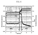
- FIG. 6 is a graph showing a result of a SIMS analysis on a sample in which a silicon dioxide film is formed by thermally oxidizing an upper part of SiC.
- the transition layer is herein a region at the interface between the SiC layer and the oxide film (including a film containing oxygen such as an oxynitride film) in which the content of carbon varies.
- the transition layer 8 is a region between a falling point A of the 18 O intensity and the maximum point B of the 13 C intensity.
- each of the contents of the three components, Si, O and C changes continuously.
- This region includes a large amount of defects causing interface traps.
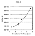
- FIG. 7 is a graph showing a correlation between the thickness of the transition layer and the total number of interface traps.
- data for the transition layer thickness of 3 nm or more was obtained by a conventional method.
- the number of interface traps was calculated by forming an MOS diode using the same oxide film as that used in the measurement in FIG. 6 and performing a CV analysis.
- the thermal oxide film was formed on a (0001) plane of 4H-SiC.
- the thickness of the transition layer 8 in the SiC-thermal oxide film interface portion is 1 nm or less, and the total trap number is 7 ⁇ 10 11 cm -2 . Accordingly, the electric characteristics in the SiC-thermal oxide film interface portion are improved, so that the channel mobility is increased. In this case, the channel mobility has a value of 60 cm 2 /(V ⁇ s).
- the oxide film is formed on the 4H-SiC (0001) plane in this embodiment.
- an oxide film having an excellent SiC-oxide film interface can be formed on other crystal planes.
- the first insulating film 2 is made thin, so that the thickness of the transition layer 8 formed on the SiC substrate 1 is kept small. Accordingly, the number of traps can be reduced.
- the number of traps can be further reduced.
- a thermal oxide film containing a trace amount (e.g., mole fraction of 0.1 % or less) of nitrogen is used as the first insulating film 2, the number of traps can be further reduced.
- the band in the transition layer 8 changes continuously.
- the thickness of the transition layer 8 is about 0.5 nm. In other words, the distance of transition from the nonconduction region to the conduction region in the SiC-insulating film interface portion is about 0.5 nm or more.
- the first cap layer 3 prevents oxygen from diffusing into the first insulating film 2 and the SiC layer 1 in subsequent heat treatment. If the first cap layer 3 is an oxynitride film having a N content of about 10 to 50 %, the occurrence of a stress in the oxynitride film is suppressed, so that the defect density is reduced.
- the first cap layer 3 preferably has a thickness of 0.5 to 10 nm. Then, the function as a cap is exhibited, and in addition, it is possible to suppress the increase of the influence of defects due to an excessive large thickness.
- the second insulating film 4 is formed by a CVD process so that the insulating films have a thickness of about 150 nm or more.
- the second insulating film 4 suppresses the occurrence of leakage current, thus ensuring the reliability of the device.
- the second insulating film 4 preferably has a thickness of 50 to 200 nm.
- the second insulating film 4 may be made of an oxynitride film, a nitride film or a high-dielectric-constant material, other than an oxide film. If the second insulating film 4 is made of a high-dielectric-constant material, leakage current is suppressed. In addition, the capacitance of the insulating film increases with high reliability maintained, so that the value of transconductance increases.
- the second cap layer 5 is preferably a nitride film with a thickness of 0.5 to 10 nm. Then, it is possible to prevent an impurity from diffusing in a region extending from the gate electrode 7 to the second insulating film 4 , during the formation of the gate electrode 7 .
- This impurity is a metal in a case where the gate electrode is made of a metal, and is boron (B) or phosphorus (P) in a case where the gate electrode is made of polysilicon.
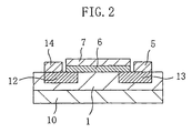
- FIG. 2 is a cross-sectional view showing a structure of the semiconductor device of the first embodiment.
- the semiconductor device of this embodiment includes: an SiC substrate 10 ; a p-type SiC layer 1 formed in an upper part of the SiC substrate 10 ; a gate insulating film 6 formed over the SiC layer 1 with a transition layer 8 interposed therebetween; a gate electrode 7 formed on the gate insulating film 6 ; source and drain regions 12 and 13 respectively formed below the sides of the gate insulating 6 and the gate electrode 7 ; and source and drain electrodes 14 and 15 formed on the source and drain regions 12 and 13 , respectively.
- the SiC substrate 10 may be either a p-type semiconductor or an n-type semiconductor.
- a substrate made of an insulator may be used instead of the SiC substrate 10 .
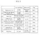
- FIG. 3 is a table showing conditions for a process of forming the gate insulating film of the semiconductor device of the first embodiment.
- step ST1 the temperature of the SiC layer 1 is increased to 1300 °C under a reduced-pressure atmosphere with silane introduced.
- the temperature may be increased without the introduction of silane because the sublimation rate of SiC is relatively low under a reduced-pressure atmosphere.
- step ST2 oxygen is supplied at 1.4 ⁇ 10 2 Pa or less onto the SiC layer 1, thereby forming a first insulating film 2 which is a thermal oxide film with a thickness of about 5 nm.
- the partial pressure of oxygen is set at 1.4 ⁇ 10 2 Pa or less, so that the first insulating film can be formed with its thickness controlled sufficiently even at a high temperature of about 1300 °C. If the first insulating film 2 is formed by an MBE process, the interface portion is controlled easily, so that atom layers are also controlled easily.
- a first insulating film having a nitrogen content of 10 % or less can be formed. In this manner, by having a trace amount of nitrogen contained in the thermal oxide film, it is possible to prevent defects from occurring in the oxide film.
- the upper part of the SiC substrate 1 may be exposed to an atmosphere containing an oxidizing gas and silane at a partial pressure of 1.4 ⁇ 10 Pa or less controlled into a pulse form, using CVD apparatus.
- the first insulating film 2 having an interface portion with sharp change between the SiC substrate 1 and the first insulating film 2 can be formed.
- Si can be supplied onto the SiC substrate by introducing silane, so that a thermal oxide film with good quality can be formed without excessively oxidizing the upper part of the SiC substrate 1 during the thermal oxidation.
- An UV ozone cleaning process may be performed on the surface of the SiC layer 1 at a temperature of 800 to 1000 °C before the formation of the first insulating film 2 .
- step ST3 annealing is performed at a temperature of 1300 °C on the substrate under a carbon monoxide atmosphere or an oxygen atmosphere at 3.9 ⁇ 10 4 Pa, thus improving the quality of the interface portion.
- the annealing is performed at a temperature of 600 to 1400 °C with carbon monoxide or oxygen at atmospheric pressure or less supplied for three hours or less, thus suppressing the occurrence of defects.
- step ST4 the substrate is placed in CVD apparatus, and silane and ammonia at 66.5 Pa are supplied onto the first insulating film 2 at a temperature of 900 °C for 10 minutes, thereby forming a first cap layer 3 which is a nitride film with a thickness of about 5 nm.
- the temperature is set within the range from 600 to 1000 °C and lower than the temperature for forming the first insulating film shown in step ST2, and the partial pressure of silane is set at 1.4 ⁇ 10 2 Pa or less. In this manner, the number of defects occurring in the insulating film is reduced to a minimum. In this step, in order to prevent the occurrence of defects, the temperature in the apparatus is not returned to room temperature.
- nitrous oxide having a flow rate of 10 % or less of the total flow rate is added to the silane gas and the ammoniacal gas, an oxynitride film having a nitrogen content of 10 to 30 % can be formed.
- step ST5 dichlorosilane and nitrous oxide at 6.65 ⁇ 10 Pa are supplied onto the first cap layer 3 by a CVD process at a temperature of 800 °C for 30 minutes, thereby forming a second insulating film 4 which is an oxide film deposited to a thickness of about 130 nm.
- the second insulating film 4 may be made of a material as a combination of SiO 2 , Si 3 N 4 , SrTiO 3 , Al 2 O 3 , Y 2 O 3 , La 2 O 3 , TaO 5 , TiO 2 , HfO 2 , and ZrO 2 , for example, or another material may be contained therein.
- the second insulating film 4 may be formed at a temperature in the range from 600 to 800 °C and lower than the temperature for forming the first cap layer 3 and the annealing temperature, the quality of the insulating films can be maintained.
- step ST6 heat treatment is performed at a temperature of 800 °C in a nitrogen monoxide atmosphere at 3.4 ⁇ 10 4 Pa for an hour.
- step ST7 silane and ammonia at 1.4 ⁇ 10 Pa are supplied onto the second insulating film 4 at a temperature of 800 °C for 10 minutes, thereby forming a second cap layer 5 which is a nitride film with a thickness of about 10 nm.
- step ST8 the temperature of the substrate is reduced to room temperature, thereby obtaining a gate insulating film 6 made up of the first insulating film 2 , the first cap layer 3 , the second insulating film 4 and the second cap layer 5.
- the gate insulating film 6 includes: the first insulating film 2 with a thickness of 0.5 nm to 20 nm obtained by thermal oxidation of the SiC layer 1; and the second insulating film 4 with a thickness of 5 nm to 200 nm deposited by, for example, a CVD process.
- the first insulating film 2 has a thickness smaller than that of a conventional thermal oxide film. Accordingly, the interface portion between the SiC layer 1 and the first insulating film 2 is controlled more easily than in a conventional device. Accordingly, the thickness of the transition layer in the interface portion between the SiC layer 1 and the first insulating film 2 can be reduced to 1 nm or less, thus suppressing the occurrence of interface state.
- the POA process such as the annealing shown in step ST4 makes it easier to clean carbon remaining in the first insulating film 2 and near the interface portion between the SiC layer 1 and the first insulating film 2 for uniformity in the interface portion.
- the second insulating film 4 allows the total thickness of the gate insulating film 6 to be about 150 nm or more which is necessary as the thickness of a gate insulating film of a low-loss power semiconductor device.
- FIG. 4 is a cross-sectional view showing a structure of the portion including the gate insulating film and its vicinity in the semiconductor device of the second embodiment.
- an n-channel region 28 is defined in an upper part of an p-type SiC layer 21 , a gate insulating film 26 including: a first insulating film 22, which is a thermal oxide film with a thickness of about 5 nm; a first cap layer 23, which is an oxynitride film with a thickness of about 5 nm; a second insulating film 24 , which is an oxide film deposited to a thickness of about 130 nm; and a second cap layer 25, which is an oxynitride film with a thickness of about 5 nm, is formed on the n-channel region 28, and a gate electrode 27 is formed on the gate insulating film 26.
- a transition layer 29 with a thickness of 1 nm or less is interposed between the SiC layer 1 and the first insulating film 2 .
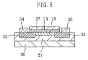
- FIG. 5 is a cross-sectional view showing a structure of the semiconductor device of the second embodiment.
- the semiconductor device of this embodiment includes: an n-type SiC substrate 20 ; the p-type SiC layer 21 formed in an upper part of the SiC substrate 20; an n-channel region 28 defined in an upper part of the SiC layer 21; the gate insulating film 26 formed over the channel region 28 with the transition layer 29 interposed therebetween; the gate electrode 27 formed on the gate insulating film 26 ; source and drain regions 32 and 33 formed in the SiC substrate 20 respectively located below the sides of the gate insulating 26 and the gate electrode 27 ; and source and drain electrodes 34 and 35 formed on the source and drain regions 32 and 33 , respectively.
- a method for forming the semiconductor device of this embodiment is the same as that described in the first embodiment except that the n-channel region 28 is formed in the upper part of the p-type SiC layer 21 .
- the effects obtained by forming the gate insulating film are the same as in the first embodiment.
- This embodiment is characterized in that the gate insulating film described in the first embodiment is formed on the ⁇ -doped layer.
- the structure of this gate insulating film is the same as in the first embodiment, and thus the description thereof will be herein omitted.
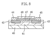
- FIG. 8 is a cross-sectional view showing a structure of a semiconductor device according to this third embodiment.
- the semiconductor device of this embodiment includes: an n-type SiC substrate 40 ; a p-type SiC layer 41 formed in an upper part of the SiC substrate 40; a channel region 46 defined in an upper part of the p-type SiC layer 41 and having a ⁇ -doped layer; a gate insulating film 47 formed on the channel region 46 ; a gate electrode 48 formed on the gate insulating film 47 ; source and drain regions 42 and 43 formed in the SiC layer 41 respectively located below the sides of the gate insulating 47 and the gate electrode 48 ; and source and drain electrodes 44 and 45 formed on the source and drain regions 42 and 43 , respectively.
- a method for forming a semiconductor device is the same as that of the first embodiment except that the channel region 46 having the ⁇ -doped layer is formed in the upper part of the p-type SiC layer 41 .
- the effects obtained by forming the gate insulating film are the same as in the first embodiment.
- This embodiment is characterized in that the gate insulating film described in the first embodiment is used as a gate insulating film of a vertical MISFET.
- the structure of this gate insulating film is the same as in the first embodiment, and thus the description thereof will be herein omitted.
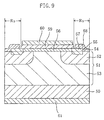
- FIG. 9 is a cross-sectional view showing a structure of a vertical accumulation-type enhancement-mode MISFET according to this fourth embodiment.
- a first SiC layer 51 is formed on a SiC substrate 50.
- P-well regions 52 containing an impurity of a second conductivity type are defined in upper parts of the first SiC layer 51 .
- a drift region 53 containing an impurity of a first conductivity type (n-type) is defined in part of the first SiC layer 51 to surround the p-well regions 52.
- a second SiC layer 54 having contact holes (grooves) 55 is provided over part of the first SiC layer 51 including the drift region 53 and the two mutually separated p-well regions 52 .
- An accumulation-type channel layer 56 containing an impurity of the first conductivity type is provided in the second SiC layer 54 except for both ends thereof.
- a contact region 57 containing an impurity of the first conductivity type is defined in each of the both ends of the second SiC layer 54 to extend to part of the first SiC layer 51 located under the associated end.
- a first ohmic electrode (source electrode) 58 is provided on the contact region 57 to extend to the surface of each of the p-well regions 52 exposed at the bottom of the associated one of the contact holes 55 .
- a gate insulating film 59 is provided on the accumulation-type channel layer 56 in the second SiC layer 54 to cover part of the contact region 57 including the boundary between the contact region 57 and the accumulation-type channel layer 56 .
- the gate insulating film 59 has the same configuration as that in the first embodiment.
- a gate electrode 60 is provided on the gate insulating film 59 .
- a second ohmic electrode (drain electrode) 61 is provided on a face (bottom face) of the SiC substrate 50 opposite to the principal surface thereof.
- the semiconductor device of this embodiment can be formed by a well-known fabrication method except for the process of forming the gate insulating film 59 .
- the method for forming the gate insulating film 59 is the same as in the first embodiment.
- the effects obtained by forming the gate insulating film 59 are the same as in the first embodiment.
- the accumulation-type enhancement-mode transistor is described as an example of a vertical MISFET.
- the present invention is also applicable to inversion-type enhancement-mode transistors.
- a thermal oxide film is formed by wet oxidation of a SiC layer
- the SiC layer is exposed to an oxygen atmosphere containing water vapor at a high concentration.
- the interface state density is suppressed to 5 ⁇ 10 11 cm -2 eV -1 or less.
- the resultant thermal oxide film contains hydrogen at a high concentration and has a low density, so that the dielectric breakdown voltage thereof is low. Accordingly, it is considered that the thermal oxide film obtained by wet oxidation lacks reliability.
- a thermal oxide film is formed by performing dry oxidation on a SiC layer
- no water vapor is introduced and the SiC layer is exposed to an oxygen atmosphere having a water vapor partial pressure of 20 % or less of the total pressure.
- the SiC layer is preferably exposed to an atmosphere having a water vapor pressure of 10 % or less of the total pressure.
- the thermal oxide film thus formed has a low concentration of hydrogen and has a high density. Accordingly, the thermal oxide film obtained by dry oxidation has a film property superior to that obtained by wet oxidation. However, in the thermal oxide film obtained by dry oxidation, a high concentration of carbon remains in an interface region between the thermal oxide film and the SiC substrate, so that the interface state density is larger than or equal to 1 ⁇ 10 12 cm -2 eV -1 .
- the thermal oxide film formed by dry oxidation is oxidized again in a wet atmosphere at a temperature lower than a temperature for dry oxidation, the density of interface state formed in the vicinity of the conduction band in the band gap can be reduced.
- a thermal oxide film is formed by performing dry oxidation on an upper part of a SiC layer, it is difficult to reduce the thickness of a transition layer at the interface between the thermal oxide film and silicon carbide.
- the oxide film formed by dry oxidation is dense and has a low defect density, this film is suitable for a gate insulating film.
- the present inventors invented a method for reducing the thickness of the transition layer by forming an oxide film having an excellent film property through dry oxidation of an upper portion of a SiC layer and then thermally oxidizing the oxide film under given conditions.
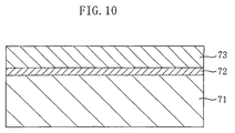
- FIG. 10 is a cross-sectional view showing a structure of the portion including the gate insulating film and its vicinity in the semiconductor device of the fifth embodiment.
- a thermal oxide film 73 is formed on a SiC substrate 71 with a transition layer 72 interposed therebetween.
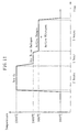
- FIG. 11 is a timing chart showing conditions for forming the gate insulating film of the semiconductor device and for performing annealing, in the fifth embodiment.
- the SiC substrate 71 (shown in FIG. 10 ) is placed in an oxygen atmosphere at a temperature of 500 °C with a 4H-SiC (0001) Si-face oriented as the principal surface. Then, the temperature of the SiC substrate 71 is increased to a temperature of 1300 °C and then thermal oxidation (dry oxidation) is performed for two hours. As a result, a thermal oxide film 73 with a thickness of 40 nm serving as a gate insulating film is formed on the 4H-SiC (0001) Si-face of the SiC substrate 71 . Then, preannealing is performed under a hydrogen atmosphere at a temperature of 1000 °C for an hour. By performing the preannealing, carbon remaining in the transition layer 72 and its vicinity can be released therefrom. Subsequently, the temperature is decreased to 900 °C with the hydrogen atmosphere maintained.
- the substrate is exposed to an atmosphere containing molecules including oxygen at a temperature of 900 °C for three hours, thereby performing annealing.
- the active oxygen is herein oxygen radicals or reactive molecules including oxygen such as nitride monoxide.
- the oxygen radicals can be generated by irradiating molecules including oxygen such as ozone with UV light or introducing the molecules into plasma.
- the active nitrogen is herein nitrogen radicals or reactive molecules including nitrogen such as nitride monoxide.
- the nitrogen radicals can be generated by irradiating nitrogen molecules or molecules including nitrogen such as ammonia with UV light or introducing the molecules into plasma.
- the active nitrogen exhibits a nitrogen passivation effect.
- the transition layer 72 With a thickness of 1 nm or less is formed between the SiC substrate 71 and the thermal oxide film 73 as shown in FIG. 10 .
- the transition layer 72 has a thickness smaller than the conventional film, so that the change in the interface between the SiC substrate 71 and the thermal oxide film 73 becomes sharper.
- the thermal oxide film as described above can be used as a gate insulating film of an inversion-type enhancement-mode semiconductor device as shown in FIG. 2 , an accumulation-type enhancement-mode semiconductor device as shown in FIG. 5, a semiconductor device using a ⁇ -doped layer as shown in FIG. 8 , and a vertical semiconductor device as shown in FIG. 9 .
- the structures of these semiconductor devices except for the gate insulating film are the same as those described in the first through fourth embodiments, and the description thereof is omitted.
- the thermal oxide film of this embodiment is formed on a 4H-SiC (0001) Si-face and is used as a gate insulating film of an inversion-type enhancement-mode insulated-gate silicon-carbide MOSFET, the effective channel mobility is increased to 50 cm 2 /(V ⁇ s) or more.
- the thickness of the transition layer can be kept at 1 nm or less.
- the concentration of hydrogen contained in the gate insulating film can be lowered, so that the density of the gate insulating film can be increased. Accordingly, a low-loss semiconductor device exhibiting a high breakdown voltage, high reliability, high channel conductance and a low ON resistance can be obtained.
- the heat treatment in this embodiment is preferably applied to a thermal oxide film with a thickness of 20 nm or less.
- a thermal oxide film with a thickness of 20 nm or less is formed by dry oxidation and then is subjected to given heat treatment, and then an oxide and a nitride are deposited to necessary thicknesses on the thermal oxide film.
- the gate insulating film thus formed can enhance the reliability and improve the quality.
- preannealing is performed in an atmosphere containing halogen, instead of a hydrogen atmosphere used in the fifth embodiment.
- This preannealing is performed at a temperature of 1000 °C for 30 minutes. The temperature is decreased to 900 °C with the halogen-containing atmosphere maintained.
- halogen radicals may be generated as active halogen, or a gas containing halogen such as silicon tetrachloride, trichlorosilane and dichlorosilane may be used.
- the thermal oxide film of this embodiment is formed on a 4H-SiC (0001) Si-face and is used as a gate insulating film of an inversion-type enhancement-mode insulated-gate silicon-carbide MOSFET, the effective channel mobility is increased to 50 cm 2 /(V ⁇ s) or more.
- the thermal oxide film as described above can be used as a gate insulating film of an inversion-type enhancement-mode semiconductor device as shown in FIG. 2 , an accumulation-type enhancement-mode semiconductor device as shown in FIG. 5 , a semiconductor device using a ⁇ -doped layer as shown in FIG. 8 , and a vertical semiconductor device as shown in FIG. 9 .
- the structures of these semiconductor devices except for the gate insulating film are the same as those described above, and the description of the structure of the semiconductor device and the fabrication method will be herein omitted.
- the thickness of the transition layer can be kept at 1 nm or less.
- the concentration of hydrogen contained in the gate insulating film can be lowered, so that the density of the gate insulating film can be increased. Accordingly, a low-loss semiconductor device exhibiting a high breakdown strength, high reliability, high channel conductance and a low ON resistance can be obtained.
- the thermal oxide film of this embodiment is formed on a 4H-SiC (0001) Si-face and is used as a gate insulating film of an inversion-type enhancement-mode insulated-gate silicon-carbide MOSFET, the effective channel mobility is increased to 50 cm 2 /(V ⁇ s) or more.
- the heat treatment in this embodiment is preferably performed on a thermal oxide film with a thickness of 20 nm or less.
- a thermal oxide film with a thickness of 20 nm or less is formed by dry oxidation and then is subjected to given heat treatment, and then an oxide and a nitride are deposited to necessary thicknesses on the thermal oxide film.
- the gate insulating film thus formed can enhance the reliability and improve the quality.
- an insulated-gate transistor for use as a commercial power device is designed to have various structures for the purpose of withstanding an inverse voltage, or passing rated current with a low ON resistance. Therefore, the insulated-gate transistor of the present invention is not limited to the structures described in the first through sixth embodiments.
- the present invention is applicable to an insulated-gate transistor having a planar RESURF structure, a vertical insulated-gate transistor and a trench-gate-type insulated-gate transistor. In the case of these transistors, the same effects as those obtained with the gate insulating films of the first through sixth embodiments are also obtained.
- the present invention is also applicable to insulated-gate semiconductor devices such as a DMIS, a trench-isolation-type MISFET and an IGBT (insulated-gate bipolar transistor) as well as the semiconductor devices described in the first through sixth embodiments.
- insulated-gate semiconductor devices such as a DMIS, a trench-isolation-type MISFET and an IGBT (insulated-gate bipolar transistor) as well as the semiconductor devices described in the first through sixth embodiments.
- the gate insulating film is made up of the first insulating film, the second insulating film, the first cap layer and the second cap layer.
- the second cap layer is not formed, if the second insulating film is an oxynitride film in particular, the second insulating film prevents metal from diffusing during the formation of the gate electrode. Accordingly, the same effects as in the case where the second cap layer is formed are attained.
- the second insulating film of the first through fourth embodiments is formed by a plasma CVD process, the same effects as in the first through fourth embodiments are attained.
- An inventive semiconductor device and an inventive method for fabricating the device are used as/for a power device incorporated in electronic equipment and, in particular, are applied to devices such as a planar MISFET, a MISFET having a ⁇ -doped layer or a vertical MISFET and a method for fabricating the devices.
Landscapes
- Formation Of Insulating Films (AREA)
- Insulated Gate Type Field-Effect Transistor (AREA)
Applications Claiming Priority (3)
| Application Number | Priority Date | Filing Date | Title |
|---|---|---|---|
| JP2001366767 | 2001-11-30 | ||
| JP2001366767 | 2001-11-30 | ||
| PCT/JP2002/012396 WO2003047000A1 (en) | 2001-11-30 | 2002-11-27 | Semiconductor device and production method therefor |
Publications (3)
| Publication Number | Publication Date |
|---|---|
| EP1463121A1 true EP1463121A1 (de) | 2004-09-29 |
| EP1463121A4 EP1463121A4 (de) | 2008-02-20 |
| EP1463121B1 EP1463121B1 (de) | 2011-04-20 |
Family
ID=19176619
Family Applications (1)
| Application Number | Title | Priority Date | Filing Date |
|---|---|---|---|
| EP02783666A Expired - Lifetime EP1463121B1 (de) | 2001-11-30 | 2002-11-27 | Halbleiterbauelement und herstellungsverfahren dafür |
Country Status (7)
| Country | Link |
|---|---|
| US (1) | US7816688B2 (de) |
| EP (1) | EP1463121B1 (de) |
| JP (1) | JP4647211B2 (de) |
| CN (1) | CN1599961A (de) |
| AU (1) | AU2002349589A1 (de) |
| DE (1) | DE60239828D1 (de) |
| WO (1) | WO2003047000A1 (de) |
Cited By (4)
| Publication number | Priority date | Publication date | Assignee | Title |
|---|---|---|---|---|
| WO2007040709A1 (en) * | 2005-09-16 | 2007-04-12 | Cree, Inc. | Methods of fabricating oxide layers on silicon carbide layers utilizing atomic oxygen |
| EP2884524A4 (de) * | 2012-08-07 | 2016-04-20 | Sumitomo Electric Industries | Siliciumcarbid-halbleiterbauelement und herstellungsverfahren dafür |
| EP3223300A1 (de) * | 2010-03-12 | 2017-09-27 | Sumitomo Electric Industries, Ltd. | Siliciumcarbid-halbleiterbauelement und verfahren zur herstellung davon |
| FR3091618A1 (fr) * | 2019-01-09 | 2020-07-10 | Soitec | Procédé de fabrication d’un substrat receveur pour une structure de type semi-conducteur sur isolant pour applications radiofrequences et procédé de fabrication d’une telle structure |
Families Citing this family (370)
| Publication number | Priority date | Publication date | Assignee | Title |
|---|---|---|---|---|
| US8546884B2 (en) * | 2002-10-29 | 2013-10-01 | Avago Technologies General Ip (Singapore) Pte. Ltd. | High value resistors in gallium arsenide |
| JP2005041835A (ja) * | 2003-07-24 | 2005-02-17 | Fuji Xerox Co Ltd | カーボンナノチューブ構造体、その製造方法、カーボンナノチューブ転写体および溶液 |
| US7709403B2 (en) | 2003-10-09 | 2010-05-04 | Panasonic Corporation | Silicon carbide-oxide layered structure, production method thereof, and semiconductor device |
| JP4676694B2 (ja) * | 2003-12-15 | 2011-04-27 | ルネサスエレクトロニクス株式会社 | 積層構造体並びに半導体装置及びその製造方法 |
| JP4549167B2 (ja) * | 2004-11-25 | 2010-09-22 | 三菱電機株式会社 | 炭化珪素半導体装置の製造方法 |
| JP2007012684A (ja) * | 2005-06-28 | 2007-01-18 | Mitsubishi Electric Corp | 半導体装置とゲート酸化膜の製造方法 |
| KR101245899B1 (ko) * | 2006-01-30 | 2013-03-20 | 스미토모덴키고교가부시키가이샤 | 탄화규소 반도체 장치의 제조 방법 |
| JP5519901B2 (ja) * | 2007-07-04 | 2014-06-11 | 三菱電機株式会社 | 炭化珪素電界効果型トランジスタ及びその製造方法 |
| JP5057903B2 (ja) * | 2007-09-06 | 2012-10-24 | 三菱電機株式会社 | 炭化珪素半導体装置の製造方法 |
| JP5100329B2 (ja) * | 2007-11-22 | 2012-12-19 | 三菱電機株式会社 | 半導体装置 |
| JP2010003868A (ja) * | 2008-06-20 | 2010-01-07 | Sanyo Electric Co Ltd | 撮像装置 |
| US9394608B2 (en) | 2009-04-06 | 2016-07-19 | Asm America, Inc. | Semiconductor processing reactor and components thereof |
| JP5197474B2 (ja) * | 2009-04-17 | 2013-05-15 | 三菱電機株式会社 | 炭化珪素半導体装置の製造方法 |
| US8802201B2 (en) * | 2009-08-14 | 2014-08-12 | Asm America, Inc. | Systems and methods for thin-film deposition of metal oxides using excited nitrogen-oxygen species |
| CN106098539B (zh) | 2009-09-07 | 2019-02-22 | 罗姆股份有限公司 | 半导体装置 |
| US8242030B2 (en) * | 2009-09-25 | 2012-08-14 | International Business Machines Corporation | Activation of graphene buffer layers on silicon carbide by ultra low temperature oxidation |
| JP5126240B2 (ja) * | 2010-01-15 | 2013-01-23 | 三菱電機株式会社 | 炭化珪素半導体装置の製造方法 |
| JP5584823B2 (ja) * | 2011-03-29 | 2014-09-03 | 株式会社日立製作所 | 炭化珪素半導体装置 |
| US9312155B2 (en) | 2011-06-06 | 2016-04-12 | Asm Japan K.K. | High-throughput semiconductor-processing apparatus equipped with multiple dual-chamber modules |
| JP5733623B2 (ja) | 2011-06-10 | 2015-06-10 | 国立大学法人九州大学 | 半導体装置の製造方法 |
| JP2013008894A (ja) * | 2011-06-27 | 2013-01-10 | Saitama Univ | 炭化珪素半導体を用いたmos構造およびその酸化膜形成方法 |
| US10854498B2 (en) | 2011-07-15 | 2020-12-01 | Asm Ip Holding B.V. | Wafer-supporting device and method for producing same |
| US20130023129A1 (en) | 2011-07-20 | 2013-01-24 | Asm America, Inc. | Pressure transmitter for a semiconductor processing environment |
| US9017481B1 (en) | 2011-10-28 | 2015-04-28 | Asm America, Inc. | Process feed management for semiconductor substrate processing |
| WO2013145023A1 (ja) * | 2012-03-30 | 2013-10-03 | 株式会社日立製作所 | 電界効果型炭化珪素トランジスタ |
| US10714315B2 (en) | 2012-10-12 | 2020-07-14 | Asm Ip Holdings B.V. | Semiconductor reaction chamber showerhead |
| JP6024962B2 (ja) * | 2012-10-29 | 2016-11-16 | 株式会社明電舎 | 半導体装置製造方法 |
| JP6088804B2 (ja) * | 2012-11-16 | 2017-03-01 | 富士電機株式会社 | 炭化珪素半導体装置および炭化珪素半導体装置の製造方法 |
| US20160376700A1 (en) | 2013-02-01 | 2016-12-29 | Asm Ip Holding B.V. | System for treatment of deposition reactor |
| JP6168945B2 (ja) * | 2013-09-20 | 2017-07-26 | 株式会社東芝 | 半導体装置およびその製造方法 |
| JP2015115374A (ja) * | 2013-12-09 | 2015-06-22 | 富士電機株式会社 | 炭化珪素半導体装置の製造方法 |
| CN104810368B (zh) * | 2014-01-28 | 2017-12-29 | 中芯国际集成电路制造(上海)有限公司 | Cmos晶体管及其形成方法 |
| US10683571B2 (en) | 2014-02-25 | 2020-06-16 | Asm Ip Holding B.V. | Gas supply manifold and method of supplying gases to chamber using same |
| US10167557B2 (en) | 2014-03-18 | 2019-01-01 | Asm Ip Holding B.V. | Gas distribution system, reactor including the system, and methods of using the same |
| US11015245B2 (en) | 2014-03-19 | 2021-05-25 | Asm Ip Holding B.V. | Gas-phase reactor and system having exhaust plenum and components thereof |
| US10858737B2 (en) | 2014-07-28 | 2020-12-08 | Asm Ip Holding B.V. | Showerhead assembly and components thereof |
| US9890456B2 (en) | 2014-08-21 | 2018-02-13 | Asm Ip Holding B.V. | Method and system for in situ formation of gas-phase compounds |
| US9657845B2 (en) | 2014-10-07 | 2017-05-23 | Asm Ip Holding B.V. | Variable conductance gas distribution apparatus and method |
| US10941490B2 (en) | 2014-10-07 | 2021-03-09 | Asm Ip Holding B.V. | Multiple temperature range susceptor, assembly, reactor and system including the susceptor, and methods of using the same |
| JP6335334B2 (ja) * | 2015-01-09 | 2018-05-30 | 株式会社日立製作所 | パワー半導体素子、パワーモジュール、および電力変換装置 |
| CN104658903A (zh) * | 2015-01-30 | 2015-05-27 | 株洲南车时代电气股份有限公司 | 一种制备SiC MOSFET栅氧化层的方法 |
| CN104637801A (zh) * | 2015-01-30 | 2015-05-20 | 株洲南车时代电气股份有限公司 | 一种制备SiC MOSFET栅氧化层的方法 |
| US10276355B2 (en) | 2015-03-12 | 2019-04-30 | Asm Ip Holding B.V. | Multi-zone reactor, system including the reactor, and method of using the same |
| JP6526549B2 (ja) * | 2015-03-24 | 2019-06-05 | 株式会社東芝 | 半導体装置、インバータ回路、駆動装置、車両、及び、昇降機 |
| US10458018B2 (en) | 2015-06-26 | 2019-10-29 | Asm Ip Holding B.V. | Structures including metal carbide material, devices including the structures, and methods of forming same |
| US10600673B2 (en) | 2015-07-07 | 2020-03-24 | Asm Ip Holding B.V. | Magnetic susceptor to baseplate seal |
| US10211308B2 (en) | 2015-10-21 | 2019-02-19 | Asm Ip Holding B.V. | NbMC layers |
| US11139308B2 (en) | 2015-12-29 | 2021-10-05 | Asm Ip Holding B.V. | Atomic layer deposition of III-V compounds to form V-NAND devices |
| US10529554B2 (en) | 2016-02-19 | 2020-01-07 | Asm Ip Holding B.V. | Method for forming silicon nitride film selectively on sidewalls or flat surfaces of trenches |
| US10343920B2 (en) | 2016-03-18 | 2019-07-09 | Asm Ip Holding B.V. | Aligned carbon nanotubes |
| US10190213B2 (en) | 2016-04-21 | 2019-01-29 | Asm Ip Holding B.V. | Deposition of metal borides |
| US10865475B2 (en) | 2016-04-21 | 2020-12-15 | Asm Ip Holding B.V. | Deposition of metal borides and silicides |
| US10032628B2 (en) | 2016-05-02 | 2018-07-24 | Asm Ip Holding B.V. | Source/drain performance through conformal solid state doping |
| US10367080B2 (en) | 2016-05-02 | 2019-07-30 | Asm Ip Holding B.V. | Method of forming a germanium oxynitride film |
| US11453943B2 (en) | 2016-05-25 | 2022-09-27 | Asm Ip Holding B.V. | Method for forming carbon-containing silicon/metal oxide or nitride film by ALD using silicon precursor and hydrocarbon precursor |
| JP6667809B2 (ja) | 2016-05-30 | 2020-03-18 | 株式会社東芝 | 半導体装置、インバータ回路、駆動装置、車両、及び、昇降機 |
| JP2016178336A (ja) * | 2016-06-10 | 2016-10-06 | 住友電気工業株式会社 | 半導体装置の製造方法 |
| US9859151B1 (en) | 2016-07-08 | 2018-01-02 | Asm Ip Holding B.V. | Selective film deposition method to form air gaps |
| US10612137B2 (en) | 2016-07-08 | 2020-04-07 | Asm Ip Holdings B.V. | Organic reactants for atomic layer deposition |
| US10714385B2 (en) | 2016-07-19 | 2020-07-14 | Asm Ip Holding B.V. | Selective deposition of tungsten |
| US9887082B1 (en) | 2016-07-28 | 2018-02-06 | Asm Ip Holding B.V. | Method and apparatus for filling a gap |
| KR102532607B1 (ko) | 2016-07-28 | 2023-05-15 | 에이에스엠 아이피 홀딩 비.브이. | 기판 가공 장치 및 그 동작 방법 |
| US9812320B1 (en) | 2016-07-28 | 2017-11-07 | Asm Ip Holding B.V. | Method and apparatus for filling a gap |
| US10643826B2 (en) | 2016-10-26 | 2020-05-05 | Asm Ip Holdings B.V. | Methods for thermally calibrating reaction chambers |
| US11532757B2 (en) | 2016-10-27 | 2022-12-20 | Asm Ip Holding B.V. | Deposition of charge trapping layers |
| US10229833B2 (en) | 2016-11-01 | 2019-03-12 | Asm Ip Holding B.V. | Methods for forming a transition metal nitride film on a substrate by atomic layer deposition and related semiconductor device structures |
| US10714350B2 (en) | 2016-11-01 | 2020-07-14 | ASM IP Holdings, B.V. | Methods for forming a transition metal niobium nitride film on a substrate by atomic layer deposition and related semiconductor device structures |
| US10643904B2 (en) | 2016-11-01 | 2020-05-05 | Asm Ip Holdings B.V. | Methods for forming a semiconductor device and related semiconductor device structures |
| US10134757B2 (en) | 2016-11-07 | 2018-11-20 | Asm Ip Holding B.V. | Method of processing a substrate and a device manufactured by using the method |
| KR102546317B1 (ko) | 2016-11-15 | 2023-06-21 | 에이에스엠 아이피 홀딩 비.브이. | 기체 공급 유닛 및 이를 포함하는 기판 처리 장치 |
| KR102762543B1 (ko) | 2016-12-14 | 2025-02-05 | 에이에스엠 아이피 홀딩 비.브이. | 기판 처리 장치 |
| US11447861B2 (en) | 2016-12-15 | 2022-09-20 | Asm Ip Holding B.V. | Sequential infiltration synthesis apparatus and a method of forming a patterned structure |
| US11581186B2 (en) | 2016-12-15 | 2023-02-14 | Asm Ip Holding B.V. | Sequential infiltration synthesis apparatus |
| KR102700194B1 (ko) | 2016-12-19 | 2024-08-28 | 에이에스엠 아이피 홀딩 비.브이. | 기판 처리 장치 |
| US10269558B2 (en) | 2016-12-22 | 2019-04-23 | Asm Ip Holding B.V. | Method of forming a structure on a substrate |
| US10867788B2 (en) | 2016-12-28 | 2020-12-15 | Asm Ip Holding B.V. | Method of forming a structure on a substrate |
| US11390950B2 (en) | 2017-01-10 | 2022-07-19 | Asm Ip Holding B.V. | Reactor system and method to reduce residue buildup during a film deposition process |
| KR102427555B1 (ko) * | 2017-01-17 | 2022-08-01 | 젯트에프 프리드리히스하펜 아게 | 규소 탄화물 상에 절연 층을 제조하는 방법 |
| US10655221B2 (en) | 2017-02-09 | 2020-05-19 | Asm Ip Holding B.V. | Method for depositing oxide film by thermal ALD and PEALD |
| US10468261B2 (en) | 2017-02-15 | 2019-11-05 | Asm Ip Holding B.V. | Methods for forming a metallic film on a substrate by cyclical deposition and related semiconductor device structures |
| US10529563B2 (en) | 2017-03-29 | 2020-01-07 | Asm Ip Holdings B.V. | Method for forming doped metal oxide films on a substrate by cyclical deposition and related semiconductor device structures |
| USD876504S1 (en) | 2017-04-03 | 2020-02-25 | Asm Ip Holding B.V. | Exhaust flow control ring for semiconductor deposition apparatus |
| KR102457289B1 (ko) | 2017-04-25 | 2022-10-21 | 에이에스엠 아이피 홀딩 비.브이. | 박막 증착 방법 및 반도체 장치의 제조 방법 |
| US10770286B2 (en) | 2017-05-08 | 2020-09-08 | Asm Ip Holdings B.V. | Methods for selectively forming a silicon nitride film on a substrate and related semiconductor device structures |
| US10892156B2 (en) | 2017-05-08 | 2021-01-12 | Asm Ip Holding B.V. | Methods for forming a silicon nitride film on a substrate and related semiconductor device structures |
| US12040200B2 (en) | 2017-06-20 | 2024-07-16 | Asm Ip Holding B.V. | Semiconductor processing apparatus and methods for calibrating a semiconductor processing apparatus |
| US11306395B2 (en) | 2017-06-28 | 2022-04-19 | Asm Ip Holding B.V. | Methods for depositing a transition metal nitride film on a substrate by atomic layer deposition and related deposition apparatus |
| US10685834B2 (en) | 2017-07-05 | 2020-06-16 | Asm Ip Holdings B.V. | Methods for forming a silicon germanium tin layer and related semiconductor device structures |
| KR20190009245A (ko) | 2017-07-18 | 2019-01-28 | 에이에스엠 아이피 홀딩 비.브이. | 반도체 소자 구조물 형성 방법 및 관련된 반도체 소자 구조물 |
| US11018002B2 (en) | 2017-07-19 | 2021-05-25 | Asm Ip Holding B.V. | Method for selectively depositing a Group IV semiconductor and related semiconductor device structures |
| US10541333B2 (en) | 2017-07-19 | 2020-01-21 | Asm Ip Holding B.V. | Method for depositing a group IV semiconductor and related semiconductor device structures |
| US11374112B2 (en) | 2017-07-19 | 2022-06-28 | Asm Ip Holding B.V. | Method for depositing a group IV semiconductor and related semiconductor device structures |
| US10590535B2 (en) | 2017-07-26 | 2020-03-17 | Asm Ip Holdings B.V. | Chemical treatment, deposition and/or infiltration apparatus and method for using the same |
| TWI815813B (zh) | 2017-08-04 | 2023-09-21 | 荷蘭商Asm智慧財產控股公司 | 用於分配反應腔內氣體的噴頭總成 |
| US10692741B2 (en) | 2017-08-08 | 2020-06-23 | Asm Ip Holdings B.V. | Radiation shield |
| US10770336B2 (en) | 2017-08-08 | 2020-09-08 | Asm Ip Holding B.V. | Substrate lift mechanism and reactor including same |
| US11139191B2 (en) | 2017-08-09 | 2021-10-05 | Asm Ip Holding B.V. | Storage apparatus for storing cassettes for substrates and processing apparatus equipped therewith |
| US11769682B2 (en) | 2017-08-09 | 2023-09-26 | Asm Ip Holding B.V. | Storage apparatus for storing cassettes for substrates and processing apparatus equipped therewith |
| US10249524B2 (en) | 2017-08-09 | 2019-04-02 | Asm Ip Holding B.V. | Cassette holder assembly for a substrate cassette and holding member for use in such assembly |
| USD900036S1 (en) | 2017-08-24 | 2020-10-27 | Asm Ip Holding B.V. | Heater electrical connector and adapter |
| US11830730B2 (en) | 2017-08-29 | 2023-11-28 | Asm Ip Holding B.V. | Layer forming method and apparatus |
| KR102491945B1 (ko) | 2017-08-30 | 2023-01-26 | 에이에스엠 아이피 홀딩 비.브이. | 기판 처리 장치 |
| US11056344B2 (en) | 2017-08-30 | 2021-07-06 | Asm Ip Holding B.V. | Layer forming method |
| US11295980B2 (en) | 2017-08-30 | 2022-04-05 | Asm Ip Holding B.V. | Methods for depositing a molybdenum metal film over a dielectric surface of a substrate by a cyclical deposition process and related semiconductor device structures |
| KR102401446B1 (ko) | 2017-08-31 | 2022-05-24 | 에이에스엠 아이피 홀딩 비.브이. | 기판 처리 장치 |
| KR102630301B1 (ko) | 2017-09-21 | 2024-01-29 | 에이에스엠 아이피 홀딩 비.브이. | 침투성 재료의 순차 침투 합성 방법 처리 및 이를 이용하여 형성된 구조물 및 장치 |
| US10844484B2 (en) | 2017-09-22 | 2020-11-24 | Asm Ip Holding B.V. | Apparatus for dispensing a vapor phase reactant to a reaction chamber and related methods |
| US10658205B2 (en) | 2017-09-28 | 2020-05-19 | Asm Ip Holdings B.V. | Chemical dispensing apparatus and methods for dispensing a chemical to a reaction chamber |
| US10403504B2 (en) | 2017-10-05 | 2019-09-03 | Asm Ip Holding B.V. | Method for selectively depositing a metallic film on a substrate |
| US10319588B2 (en) | 2017-10-10 | 2019-06-11 | Asm Ip Holding B.V. | Method for depositing a metal chalcogenide on a substrate by cyclical deposition |
| US10923344B2 (en) | 2017-10-30 | 2021-02-16 | Asm Ip Holding B.V. | Methods for forming a semiconductor structure and related semiconductor structures |
| US10910262B2 (en) | 2017-11-16 | 2021-02-02 | Asm Ip Holding B.V. | Method of selectively depositing a capping layer structure on a semiconductor device structure |
| KR102443047B1 (ko) | 2017-11-16 | 2022-09-14 | 에이에스엠 아이피 홀딩 비.브이. | 기판 처리 장치 방법 및 그에 의해 제조된 장치 |
| US11022879B2 (en) | 2017-11-24 | 2021-06-01 | Asm Ip Holding B.V. | Method of forming an enhanced unexposed photoresist layer |
| TWI791689B (zh) | 2017-11-27 | 2023-02-11 | 荷蘭商Asm智慧財產控股私人有限公司 | 包括潔淨迷你環境之裝置 |
| JP7214724B2 (ja) | 2017-11-27 | 2023-01-30 | エーエスエム アイピー ホールディング ビー.ブイ. | バッチ炉で利用されるウェハカセットを収納するための収納装置 |
| US10629749B2 (en) | 2017-11-30 | 2020-04-21 | Taiwan Semiconductor Manufacturing Co., Ltd. | Method of treating interfacial layer on silicon germanium |
| US10872771B2 (en) | 2018-01-16 | 2020-12-22 | Asm Ip Holding B. V. | Method for depositing a material film on a substrate within a reaction chamber by a cyclical deposition process and related device structures |
| KR102695659B1 (ko) | 2018-01-19 | 2024-08-14 | 에이에스엠 아이피 홀딩 비.브이. | 플라즈마 보조 증착에 의해 갭 충진 층을 증착하는 방법 |
| TWI799494B (zh) | 2018-01-19 | 2023-04-21 | 荷蘭商Asm 智慧財產控股公司 | 沈積方法 |
| USD903477S1 (en) | 2018-01-24 | 2020-12-01 | Asm Ip Holdings B.V. | Metal clamp |
| US11018047B2 (en) | 2018-01-25 | 2021-05-25 | Asm Ip Holding B.V. | Hybrid lift pin |
| USD880437S1 (en) | 2018-02-01 | 2020-04-07 | Asm Ip Holding B.V. | Gas supply plate for semiconductor manufacturing apparatus |
| US11081345B2 (en) | 2018-02-06 | 2021-08-03 | Asm Ip Holding B.V. | Method of post-deposition treatment for silicon oxide film |
| US11685991B2 (en) | 2018-02-14 | 2023-06-27 | Asm Ip Holding B.V. | Method for depositing a ruthenium-containing film on a substrate by a cyclical deposition process |
| US10896820B2 (en) | 2018-02-14 | 2021-01-19 | Asm Ip Holding B.V. | Method for depositing a ruthenium-containing film on a substrate by a cyclical deposition process |
| US10731249B2 (en) | 2018-02-15 | 2020-08-04 | Asm Ip Holding B.V. | Method of forming a transition metal containing film on a substrate by a cyclical deposition process, a method for supplying a transition metal halide compound to a reaction chamber, and related vapor deposition apparatus |
| US10658181B2 (en) | 2018-02-20 | 2020-05-19 | Asm Ip Holding B.V. | Method of spacer-defined direct patterning in semiconductor fabrication |
| KR102636427B1 (ko) | 2018-02-20 | 2024-02-13 | 에이에스엠 아이피 홀딩 비.브이. | 기판 처리 방법 및 장치 |
| US10975470B2 (en) | 2018-02-23 | 2021-04-13 | Asm Ip Holding B.V. | Apparatus for detecting or monitoring for a chemical precursor in a high temperature environment |
| JP7056232B2 (ja) * | 2018-02-28 | 2022-04-19 | 富士電機株式会社 | 炭化珪素半導体装置および炭化珪素半導体装置の製造方法 |
| US11473195B2 (en) | 2018-03-01 | 2022-10-18 | Asm Ip Holding B.V. | Semiconductor processing apparatus and a method for processing a substrate |
| US11629406B2 (en) | 2018-03-09 | 2023-04-18 | Asm Ip Holding B.V. | Semiconductor processing apparatus comprising one or more pyrometers for measuring a temperature of a substrate during transfer of the substrate |
| US11114283B2 (en) | 2018-03-16 | 2021-09-07 | Asm Ip Holding B.V. | Reactor, system including the reactor, and methods of manufacturing and using same |
| KR102646467B1 (ko) | 2018-03-27 | 2024-03-11 | 에이에스엠 아이피 홀딩 비.브이. | 기판 상에 전극을 형성하는 방법 및 전극을 포함하는 반도체 소자 구조 |
| US11230766B2 (en) | 2018-03-29 | 2022-01-25 | Asm Ip Holding B.V. | Substrate processing apparatus and method |
| US11088002B2 (en) | 2018-03-29 | 2021-08-10 | Asm Ip Holding B.V. | Substrate rack and a substrate processing system and method |
| KR102501472B1 (ko) | 2018-03-30 | 2023-02-20 | 에이에스엠 아이피 홀딩 비.브이. | 기판 처리 방법 |
| DE102018107966B4 (de) | 2018-04-04 | 2022-02-17 | Infineon Technologies Ag | Verfahren zum Bilden eines Breiter-Bandabstand-Halbleiter-Bauelements |
| KR102600229B1 (ko) | 2018-04-09 | 2023-11-10 | 에이에스엠 아이피 홀딩 비.브이. | 기판 지지 장치, 이를 포함하는 기판 처리 장치 및 기판 처리 방법 |
| TWI843623B (zh) | 2018-05-08 | 2024-05-21 | 荷蘭商Asm Ip私人控股有限公司 | 藉由循環沉積製程於基板上沉積氧化物膜之方法及相關裝置結構 |
| US12025484B2 (en) | 2018-05-08 | 2024-07-02 | Asm Ip Holding B.V. | Thin film forming method |
| US12272527B2 (en) | 2018-05-09 | 2025-04-08 | Asm Ip Holding B.V. | Apparatus for use with hydrogen radicals and method of using same |
| KR20190129718A (ko) | 2018-05-11 | 2019-11-20 | 에이에스엠 아이피 홀딩 비.브이. | 기판 상에 피도핑 금속 탄화물 막을 형성하는 방법 및 관련 반도체 소자 구조 |
| KR102596988B1 (ko) | 2018-05-28 | 2023-10-31 | 에이에스엠 아이피 홀딩 비.브이. | 기판 처리 방법 및 그에 의해 제조된 장치 |
| TWI840362B (zh) | 2018-06-04 | 2024-05-01 | 荷蘭商Asm Ip私人控股有限公司 | 水氣降低的晶圓處置腔室 |
| US11718913B2 (en) | 2018-06-04 | 2023-08-08 | Asm Ip Holding B.V. | Gas distribution system and reactor system including same |
| US11286562B2 (en) | 2018-06-08 | 2022-03-29 | Asm Ip Holding B.V. | Gas-phase chemical reactor and method of using same |
| KR102568797B1 (ko) | 2018-06-21 | 2023-08-21 | 에이에스엠 아이피 홀딩 비.브이. | 기판 처리 시스템 |
| US10797133B2 (en) | 2018-06-21 | 2020-10-06 | Asm Ip Holding B.V. | Method for depositing a phosphorus doped silicon arsenide film and related semiconductor device structures |
| TWI871083B (zh) | 2018-06-27 | 2025-01-21 | 荷蘭商Asm Ip私人控股有限公司 | 用於形成含金屬材料之循環沉積製程 |
| US11499222B2 (en) | 2018-06-27 | 2022-11-15 | Asm Ip Holding B.V. | Cyclic deposition methods for forming metal-containing material and films and structures including the metal-containing material |
| KR102686758B1 (ko) | 2018-06-29 | 2024-07-18 | 에이에스엠 아이피 홀딩 비.브이. | 박막 증착 방법 및 반도체 장치의 제조 방법 |
| US10612136B2 (en) | 2018-06-29 | 2020-04-07 | ASM IP Holding, B.V. | Temperature-controlled flange and reactor system including same |
| US10755922B2 (en) | 2018-07-03 | 2020-08-25 | Asm Ip Holding B.V. | Method for depositing silicon-free carbon-containing film as gap-fill layer by pulse plasma-assisted deposition |
| US10388513B1 (en) | 2018-07-03 | 2019-08-20 | Asm Ip Holding B.V. | Method for depositing silicon-free carbon-containing film as gap-fill layer by pulse plasma-assisted deposition |
| US10767789B2 (en) | 2018-07-16 | 2020-09-08 | Asm Ip Holding B.V. | Diaphragm valves, valve components, and methods for forming valve components |
| US11053591B2 (en) | 2018-08-06 | 2021-07-06 | Asm Ip Holding B.V. | Multi-port gas injection system and reactor system including same |
| US10883175B2 (en) | 2018-08-09 | 2021-01-05 | Asm Ip Holding B.V. | Vertical furnace for processing substrates and a liner for use therein |
| US10829852B2 (en) | 2018-08-16 | 2020-11-10 | Asm Ip Holding B.V. | Gas distribution device for a wafer processing apparatus |
| US11430674B2 (en) | 2018-08-22 | 2022-08-30 | Asm Ip Holding B.V. | Sensor array, apparatus for dispensing a vapor phase reactant to a reaction chamber and related methods |
| KR102707956B1 (ko) | 2018-09-11 | 2024-09-19 | 에이에스엠 아이피 홀딩 비.브이. | 박막 증착 방법 |
| US11024523B2 (en) | 2018-09-11 | 2021-06-01 | Asm Ip Holding B.V. | Substrate processing apparatus and method |
| US11049751B2 (en) | 2018-09-14 | 2021-06-29 | Asm Ip Holding B.V. | Cassette supply system to store and handle cassettes and processing apparatus equipped therewith |
| CN110970344B (zh) | 2018-10-01 | 2024-10-25 | Asmip控股有限公司 | 衬底保持设备、包含所述设备的系统及其使用方法 |
| US11232963B2 (en) | 2018-10-03 | 2022-01-25 | Asm Ip Holding B.V. | Substrate processing apparatus and method |
| KR102592699B1 (ko) | 2018-10-08 | 2023-10-23 | 에이에스엠 아이피 홀딩 비.브이. | 기판 지지 유닛 및 이를 포함하는 박막 증착 장치와 기판 처리 장치 |
| US10847365B2 (en) | 2018-10-11 | 2020-11-24 | Asm Ip Holding B.V. | Method of forming conformal silicon carbide film by cyclic CVD |
| US10811256B2 (en) | 2018-10-16 | 2020-10-20 | Asm Ip Holding B.V. | Method for etching a carbon-containing feature |
| KR102546322B1 (ko) | 2018-10-19 | 2023-06-21 | 에이에스엠 아이피 홀딩 비.브이. | 기판 처리 장치 및 기판 처리 방법 |
| KR102605121B1 (ko) | 2018-10-19 | 2023-11-23 | 에이에스엠 아이피 홀딩 비.브이. | 기판 처리 장치 및 기판 처리 방법 |
| USD948463S1 (en) | 2018-10-24 | 2022-04-12 | Asm Ip Holding B.V. | Susceptor for semiconductor substrate supporting apparatus |
| US12378665B2 (en) | 2018-10-26 | 2025-08-05 | Asm Ip Holding B.V. | High temperature coatings for a preclean and etch apparatus and related methods |
| CN109411343A (zh) * | 2018-10-31 | 2019-03-01 | 秦皇岛京河科学技术研究院有限公司 | 一种SiC MOSFET栅氧化层退火方法 |
| US11087997B2 (en) | 2018-10-31 | 2021-08-10 | Asm Ip Holding B.V. | Substrate processing apparatus for processing substrates |
| CN109461646B (zh) * | 2018-10-31 | 2020-11-17 | 秦皇岛京河科学技术研究院有限公司 | 一种SiC MOSFET栅氧化层退火方法 |
| KR102748291B1 (ko) | 2018-11-02 | 2024-12-31 | 에이에스엠 아이피 홀딩 비.브이. | 기판 지지 유닛 및 이를 포함하는 기판 처리 장치 |
| US11572620B2 (en) | 2018-11-06 | 2023-02-07 | Asm Ip Holding B.V. | Methods for selectively depositing an amorphous silicon film on a substrate |
| US11031242B2 (en) | 2018-11-07 | 2021-06-08 | Asm Ip Holding B.V. | Methods for depositing a boron doped silicon germanium film |
| US10818758B2 (en) | 2018-11-16 | 2020-10-27 | Asm Ip Holding B.V. | Methods for forming a metal silicate film on a substrate in a reaction chamber and related semiconductor device structures |
| US10847366B2 (en) | 2018-11-16 | 2020-11-24 | Asm Ip Holding B.V. | Methods for depositing a transition metal chalcogenide film on a substrate by a cyclical deposition process |
| US10559458B1 (en) | 2018-11-26 | 2020-02-11 | Asm Ip Holding B.V. | Method of forming oxynitride film |
| US12040199B2 (en) | 2018-11-28 | 2024-07-16 | Asm Ip Holding B.V. | Substrate processing apparatus for processing substrates |
| US11217444B2 (en) | 2018-11-30 | 2022-01-04 | Asm Ip Holding B.V. | Method for forming an ultraviolet radiation responsive metal oxide-containing film |
| KR102636428B1 (ko) | 2018-12-04 | 2024-02-13 | 에이에스엠 아이피 홀딩 비.브이. | 기판 처리 장치를 세정하는 방법 |
| US11158513B2 (en) | 2018-12-13 | 2021-10-26 | Asm Ip Holding B.V. | Methods for forming a rhenium-containing film on a substrate by a cyclical deposition process and related semiconductor device structures |
| JP7504584B2 (ja) | 2018-12-14 | 2024-06-24 | エーエスエム・アイピー・ホールディング・ベー・フェー | 窒化ガリウムの選択的堆積を用いてデバイス構造体を形成する方法及びそのためのシステム |
| TWI866480B (zh) | 2019-01-17 | 2024-12-11 | 荷蘭商Asm Ip 私人控股有限公司 | 藉由循環沈積製程於基板上形成含過渡金屬膜之方法 |
| KR102727227B1 (ko) | 2019-01-22 | 2024-11-07 | 에이에스엠 아이피 홀딩 비.브이. | 기판 처리 장치 |
| CN111524788B (zh) | 2019-02-01 | 2023-11-24 | Asm Ip私人控股有限公司 | 氧化硅的拓扑选择性膜形成的方法 |
| TWI873122B (zh) | 2019-02-20 | 2025-02-21 | 荷蘭商Asm Ip私人控股有限公司 | 填充一基板之一表面內所形成的一凹槽的方法、根據其所形成之半導體結構、及半導體處理設備 |
| TWI845607B (zh) | 2019-02-20 | 2024-06-21 | 荷蘭商Asm Ip私人控股有限公司 | 用來填充形成於基材表面內之凹部的循環沉積方法及設備 |
| KR20200102357A (ko) | 2019-02-20 | 2020-08-31 | 에이에스엠 아이피 홀딩 비.브이. | 3-d nand 응용의 플러그 충진체 증착용 장치 및 방법 |
| KR102626263B1 (ko) | 2019-02-20 | 2024-01-16 | 에이에스엠 아이피 홀딩 비.브이. | 처리 단계를 포함하는 주기적 증착 방법 및 이를 위한 장치 |
| TWI842826B (zh) | 2019-02-22 | 2024-05-21 | 荷蘭商Asm Ip私人控股有限公司 | 基材處理設備及處理基材之方法 |
| KR102782593B1 (ko) | 2019-03-08 | 2025-03-14 | 에이에스엠 아이피 홀딩 비.브이. | SiOC 층을 포함한 구조체 및 이의 형성 방법 |
| KR102762833B1 (ko) | 2019-03-08 | 2025-02-04 | 에이에스엠 아이피 홀딩 비.브이. | SiOCN 층을 포함한 구조체 및 이의 형성 방법 |
| KR102858005B1 (ko) | 2019-03-08 | 2025-09-09 | 에이에스엠 아이피 홀딩 비.브이. | 실리콘 질화물 층을 선택적으로 증착하는 방법, 및 선택적으로 증착된 실리콘 질화물 층을 포함하는 구조체 |
| JP7204547B2 (ja) | 2019-03-15 | 2023-01-16 | 株式会社東芝 | 半導体装置 |
| JP2020155698A (ja) * | 2019-03-22 | 2020-09-24 | 株式会社豊田中央研究所 | 炭化珪素半導体装置 |
| JP2020167398A (ja) | 2019-03-28 | 2020-10-08 | エーエスエム・アイピー・ホールディング・ベー・フェー | ドアオープナーおよびドアオープナーが提供される基材処理装置 |
| KR102809999B1 (ko) | 2019-04-01 | 2025-05-19 | 에이에스엠 아이피 홀딩 비.브이. | 반도체 소자를 제조하는 방법 |
| KR102897355B1 (ko) | 2019-04-19 | 2025-12-08 | 에이에스엠 아이피 홀딩 비.브이. | 층 형성 방법 및 장치 |
| KR20200125453A (ko) | 2019-04-24 | 2020-11-04 | 에이에스엠 아이피 홀딩 비.브이. | 기상 반응기 시스템 및 이를 사용하는 방법 |
| KR102869364B1 (ko) | 2019-05-07 | 2025-10-10 | 에이에스엠 아이피 홀딩 비.브이. | 비정질 탄소 중합체 막을 개질하는 방법 |
| KR102929471B1 (ko) | 2019-05-07 | 2026-02-20 | 에이에스엠 아이피 홀딩 비.브이. | 딥 튜브가 있는 화학물질 공급원 용기 |
| KR102929472B1 (ko) | 2019-05-10 | 2026-02-20 | 에이에스엠 아이피 홀딩 비.브이. | 표면 상에 재료를 증착하는 방법 및 본 방법에 따라 형성된 구조 |
| JP7598201B2 (ja) | 2019-05-16 | 2024-12-11 | エーエスエム・アイピー・ホールディング・ベー・フェー | ウェハボートハンドリング装置、縦型バッチ炉および方法 |
| JP7612342B2 (ja) | 2019-05-16 | 2025-01-14 | エーエスエム・アイピー・ホールディング・ベー・フェー | ウェハボートハンドリング装置、縦型バッチ炉および方法 |
| USD947913S1 (en) | 2019-05-17 | 2022-04-05 | Asm Ip Holding B.V. | Susceptor shaft |
| USD975665S1 (en) | 2019-05-17 | 2023-01-17 | Asm Ip Holding B.V. | Susceptor shaft |
| USD935572S1 (en) | 2019-05-24 | 2021-11-09 | Asm Ip Holding B.V. | Gas channel plate |
| USD922229S1 (en) | 2019-06-05 | 2021-06-15 | Asm Ip Holding B.V. | Device for controlling a temperature of a gas supply unit |
| KR20200141002A (ko) | 2019-06-06 | 2020-12-17 | 에이에스엠 아이피 홀딩 비.브이. | 배기 가스 분석을 포함한 기상 반응기 시스템을 사용하는 방법 |
| KR102918757B1 (ko) | 2019-06-10 | 2026-01-28 | 에이에스엠 아이피 홀딩 비.브이. | 석영 에피택셜 챔버를 세정하는 방법 |
| KR20200143254A (ko) | 2019-06-11 | 2020-12-23 | 에이에스엠 아이피 홀딩 비.브이. | 개질 가스를 사용하여 전자 구조를 형성하는 방법, 상기 방법을 수행하기 위한 시스템, 및 상기 방법을 사용하여 형성되는 구조 |
| USD944946S1 (en) | 2019-06-14 | 2022-03-01 | Asm Ip Holding B.V. | Shower plate |
| USD931978S1 (en) | 2019-06-27 | 2021-09-28 | Asm Ip Holding B.V. | Showerhead vacuum transport |
| KR102911421B1 (ko) | 2019-07-03 | 2026-01-12 | 에이에스엠 아이피 홀딩 비.브이. | 기판 처리 장치용 온도 제어 조립체 및 이를 사용하는 방법 |
| JP7499079B2 (ja) | 2019-07-09 | 2024-06-13 | エーエスエム・アイピー・ホールディング・ベー・フェー | 同軸導波管を用いたプラズマ装置、基板処理方法 |
| CN112216646B (zh) | 2019-07-10 | 2026-02-10 | Asmip私人控股有限公司 | 基板支撑组件及包括其的基板处理装置 |
| KR102895115B1 (ko) | 2019-07-16 | 2025-12-03 | 에이에스엠 아이피 홀딩 비.브이. | 기판 처리 장치 |
| KR102860110B1 (ko) | 2019-07-17 | 2025-09-16 | 에이에스엠 아이피 홀딩 비.브이. | 실리콘 게르마늄 구조를 형성하는 방법 |
| TWI826704B (zh) | 2019-07-17 | 2023-12-21 | 荷蘭商Asm Ip私人控股有限公司 | 自由基輔助引燃電漿系統和方法 |
| US11643724B2 (en) | 2019-07-18 | 2023-05-09 | Asm Ip Holding B.V. | Method of forming structures using a neutral beam |
| KR102903090B1 (ko) | 2019-07-19 | 2025-12-19 | 에이에스엠 아이피 홀딩 비.브이. | 토폴로지-제어된 비정질 탄소 중합체 막을 형성하는 방법 |
| TWI839544B (zh) | 2019-07-19 | 2024-04-21 | 荷蘭商Asm Ip私人控股有限公司 | 形成形貌受控的非晶碳聚合物膜之方法 |
| CN112309843B (zh) | 2019-07-29 | 2026-01-23 | Asmip私人控股有限公司 | 实现高掺杂剂掺入的选择性沉积方法 |
| CN112309899B (zh) | 2019-07-30 | 2025-11-14 | Asmip私人控股有限公司 | 基板处理设备 |
| CN112309900B (zh) | 2019-07-30 | 2025-11-04 | Asmip私人控股有限公司 | 基板处理设备 |
| KR20210015655A (ko) | 2019-07-30 | 2021-02-10 | 에이에스엠 아이피 홀딩 비.브이. | 기판 처리 장치 및 방법 |
| US11587814B2 (en) | 2019-07-31 | 2023-02-21 | Asm Ip Holding B.V. | Vertical batch furnace assembly |
| US11587815B2 (en) | 2019-07-31 | 2023-02-21 | Asm Ip Holding B.V. | Vertical batch furnace assembly |
| US11227782B2 (en) | 2019-07-31 | 2022-01-18 | Asm Ip Holding B.V. | Vertical batch furnace assembly |
| KR20210018759A (ko) | 2019-08-05 | 2021-02-18 | 에이에스엠 아이피 홀딩 비.브이. | 화학물질 공급원 용기를 위한 액체 레벨 센서 |
| KR20210018761A (ko) | 2019-08-09 | 2021-02-18 | 에이에스엠 아이피 홀딩 비.브이. | 냉각 장치를 포함한 히터 어셈블리 및 이를 사용하는 방법 |
| USD965044S1 (en) | 2019-08-19 | 2022-09-27 | Asm Ip Holding B.V. | Susceptor shaft |
| USD965524S1 (en) | 2019-08-19 | 2022-10-04 | Asm Ip Holding B.V. | Susceptor support |
| JP7810514B2 (ja) | 2019-08-21 | 2026-02-03 | エーエスエム・アイピー・ホールディング・ベー・フェー | 成膜原料混合ガス生成装置及び成膜装置 |
| KR20210024423A (ko) | 2019-08-22 | 2021-03-05 | 에이에스엠 아이피 홀딩 비.브이. | 홀을 구비한 구조체를 형성하기 위한 방법 |
| USD979506S1 (en) | 2019-08-22 | 2023-02-28 | Asm Ip Holding B.V. | Insulator |
| USD940837S1 (en) | 2019-08-22 | 2022-01-11 | Asm Ip Holding B.V. | Electrode |
| USD949319S1 (en) | 2019-08-22 | 2022-04-19 | Asm Ip Holding B.V. | Exhaust duct |
| USD930782S1 (en) | 2019-08-22 | 2021-09-14 | Asm Ip Holding B.V. | Gas distributor |
| US11286558B2 (en) | 2019-08-23 | 2022-03-29 | Asm Ip Holding B.V. | Methods for depositing a molybdenum nitride film on a surface of a substrate by a cyclical deposition process and related semiconductor device structures including a molybdenum nitride film |
| KR102928101B1 (ko) | 2019-08-23 | 2026-02-13 | 에이에스엠 아이피 홀딩 비.브이. | 비스(디에틸아미노)실란을 사용하여 peald에 의해 개선된 품질을 갖는 실리콘 산화물 막을 증착하기 위한 방법 |
| KR102868968B1 (ko) | 2019-09-03 | 2025-10-10 | 에이에스엠 아이피 홀딩 비.브이. | 칼코지나이드 막 및 상기 막을 포함한 구조체를 증착하기 위한 방법 및 장치 |
| KR102806450B1 (ko) | 2019-09-04 | 2025-05-12 | 에이에스엠 아이피 홀딩 비.브이. | 희생 캡핑 층을 이용한 선택적 증착 방법 |
| KR102733104B1 (ko) | 2019-09-05 | 2024-11-22 | 에이에스엠 아이피 홀딩 비.브이. | 기판 처리 장치 |
| US12469693B2 (en) | 2019-09-17 | 2025-11-11 | Asm Ip Holding B.V. | Method of forming a carbon-containing layer and structure including the layer |
| US11562901B2 (en) | 2019-09-25 | 2023-01-24 | Asm Ip Holding B.V. | Substrate processing method |
| CN112593212B (zh) | 2019-10-02 | 2023-12-22 | Asm Ip私人控股有限公司 | 通过循环等离子体增强沉积工艺形成拓扑选择性氧化硅膜的方法 |
| TWI846953B (zh) | 2019-10-08 | 2024-07-01 | 荷蘭商Asm Ip私人控股有限公司 | 基板處理裝置 |
| KR102948143B1 (ko) | 2019-10-08 | 2026-04-07 | 에이에스엠 아이피 홀딩 비.브이. | 활성 종을 이용하기 위한 가스 분배 어셈블리를 포함한 반응기 시스템 및 이를 사용하는 방법 |
| TW202128273A (zh) | 2019-10-08 | 2021-08-01 | 荷蘭商Asm Ip私人控股有限公司 | 氣體注入系統、及將材料沉積於反應室內之基板表面上的方法 |
| TWI846966B (zh) | 2019-10-10 | 2024-07-01 | 荷蘭商Asm Ip私人控股有限公司 | 形成光阻底層之方法及包括光阻底層之結構 |
| US12009241B2 (en) | 2019-10-14 | 2024-06-11 | Asm Ip Holding B.V. | Vertical batch furnace assembly with detector to detect cassette |
| TWI834919B (zh) | 2019-10-16 | 2024-03-11 | 荷蘭商Asm Ip私人控股有限公司 | 氧化矽之拓撲選擇性膜形成之方法 |
| US11637014B2 (en) | 2019-10-17 | 2023-04-25 | Asm Ip Holding B.V. | Methods for selective deposition of doped semiconductor material |
| KR102845724B1 (ko) | 2019-10-21 | 2025-08-13 | 에이에스엠 아이피 홀딩 비.브이. | 막을 선택적으로 에칭하기 위한 장치 및 방법 |
| US11996292B2 (en) | 2019-10-25 | 2024-05-28 | Asm Ip Holding B.V. | Methods for filling a gap feature on a substrate surface and related semiconductor structures |
| US11646205B2 (en) | 2019-10-29 | 2023-05-09 | Asm Ip Holding B.V. | Methods of selectively forming n-type doped material on a surface, systems for selectively forming n-type doped material, and structures formed using same |
| KR102890638B1 (ko) | 2019-11-05 | 2025-11-25 | 에이에스엠 아이피 홀딩 비.브이. | 도핑된 반도체 층을 갖는 구조체 및 이를 형성하기 위한 방법 및 시스템 |
| US11501968B2 (en) | 2019-11-15 | 2022-11-15 | Asm Ip Holding B.V. | Method for providing a semiconductor device with silicon filled gaps |
| KR102861314B1 (ko) | 2019-11-20 | 2025-09-17 | 에이에스엠 아이피 홀딩 비.브이. | 기판의 표면 상에 탄소 함유 물질을 증착하는 방법, 상기 방법을 사용하여 형성된 구조물, 및 상기 구조물을 형성하기 위한 시스템 |
| CN112951697B (zh) | 2019-11-26 | 2025-07-29 | Asmip私人控股有限公司 | 基板处理设备 |
| KR20210065848A (ko) | 2019-11-26 | 2021-06-04 | 에이에스엠 아이피 홀딩 비.브이. | 제1 유전체 표면과 제2 금속성 표면을 포함한 기판 상에 타겟 막을 선택적으로 형성하기 위한 방법 |
| CN120432376A (zh) | 2019-11-29 | 2025-08-05 | Asm Ip私人控股有限公司 | 基板处理设备 |
| CN112885692B (zh) | 2019-11-29 | 2025-08-15 | Asmip私人控股有限公司 | 基板处理设备 |
| JP7527928B2 (ja) | 2019-12-02 | 2024-08-05 | エーエスエム・アイピー・ホールディング・ベー・フェー | 基板処理装置、基板処理方法 |
| KR20210070898A (ko) | 2019-12-04 | 2021-06-15 | 에이에스엠 아이피 홀딩 비.브이. | 기판 처리 장치 |
| US11885013B2 (en) | 2019-12-17 | 2024-01-30 | Asm Ip Holding B.V. | Method of forming vanadium nitride layer and structure including the vanadium nitride layer |
| KR102943768B1 (ko) | 2019-12-19 | 2026-03-26 | 에이에스엠 아이피 홀딩 비.브이. | 기판 상의 갭 피처를 충진하는 방법 및 이와 관련된 반도체 소자 구조 |
| JP7730637B2 (ja) | 2020-01-06 | 2025-08-28 | エーエスエム・アイピー・ホールディング・ベー・フェー | ガス供給アセンブリ、その構成要素、およびこれを含む反応器システム |
| TWI887322B (zh) | 2020-01-06 | 2025-06-21 | 荷蘭商Asm Ip私人控股有限公司 | 反應器系統、抬升銷、及處理方法 |
| US11993847B2 (en) | 2020-01-08 | 2024-05-28 | Asm Ip Holding B.V. | Injector |
| KR102882467B1 (ko) | 2020-01-16 | 2025-11-05 | 에이에스엠 아이피 홀딩 비.브이. | 고 종횡비 피처를 형성하는 방법 |
| KR102675856B1 (ko) | 2020-01-20 | 2024-06-17 | 에이에스엠 아이피 홀딩 비.브이. | 박막 형성 방법 및 박막 표면 개질 방법 |
| TWI889744B (zh) | 2020-01-29 | 2025-07-11 | 荷蘭商Asm Ip私人控股有限公司 | 污染物捕集系統、及擋板堆疊 |
| TW202513845A (zh) | 2020-02-03 | 2025-04-01 | 荷蘭商Asm Ip私人控股有限公司 | 半導體裝置結構及其形成方法 |
| KR20210100010A (ko) | 2020-02-04 | 2021-08-13 | 에이에스엠 아이피 홀딩 비.브이. | 대형 물품의 투과율 측정을 위한 방법 및 장치 |
| US11776846B2 (en) | 2020-02-07 | 2023-10-03 | Asm Ip Holding B.V. | Methods for depositing gap filling fluids and related systems and devices |
| KR20210103953A (ko) | 2020-02-13 | 2021-08-24 | 에이에스엠 아이피 홀딩 비.브이. | 가스 분배 어셈블리 및 이를 사용하는 방법 |
| KR102916725B1 (ko) | 2020-02-13 | 2026-01-23 | 에이에스엠 아이피 홀딩 비.브이. | 수광 장치를 포함하는 기판 처리 장치 및 수광 장치의 교정 방법 |
| US11781243B2 (en) | 2020-02-17 | 2023-10-10 | Asm Ip Holding B.V. | Method for depositing low temperature phosphorous-doped silicon |
| TWI895326B (zh) | 2020-02-28 | 2025-09-01 | 荷蘭商Asm Ip私人控股有限公司 | 專用於零件清潔的系統 |
| KR102943116B1 (ko) | 2020-03-04 | 2026-03-23 | 에이에스엠 아이피 홀딩 비.브이. | 반응기 시스템용 정렬 고정구 |
| KR20210116240A (ko) | 2020-03-11 | 2021-09-27 | 에이에스엠 아이피 홀딩 비.브이. | 조절성 접합부를 갖는 기판 핸들링 장치 |
| US11876356B2 (en) | 2020-03-11 | 2024-01-16 | Asm Ip Holding B.V. | Lockout tagout assembly and system and method of using same |
| KR102775390B1 (ko) | 2020-03-12 | 2025-02-28 | 에이에스엠 아이피 홀딩 비.브이. | 타겟 토폴로지 프로파일을 갖는 층 구조를 제조하기 위한 방법 |
| US12173404B2 (en) | 2020-03-17 | 2024-12-24 | Asm Ip Holding B.V. | Method of depositing epitaxial material, structure formed using the method, and system for performing the method |
| KR102755229B1 (ko) | 2020-04-02 | 2025-01-14 | 에이에스엠 아이피 홀딩 비.브이. | 박막 형성 방법 |
| TWI887376B (zh) | 2020-04-03 | 2025-06-21 | 荷蘭商Asm Ip私人控股有限公司 | 半導體裝置的製造方法 |
| TWI888525B (zh) | 2020-04-08 | 2025-07-01 | 荷蘭商Asm Ip私人控股有限公司 | 用於選擇性蝕刻氧化矽膜之設備及方法 |
| KR20210128343A (ko) | 2020-04-15 | 2021-10-26 | 에이에스엠 아이피 홀딩 비.브이. | 크롬 나이트라이드 층을 형성하는 방법 및 크롬 나이트라이드 층을 포함하는 구조 |
| US11821078B2 (en) | 2020-04-15 | 2023-11-21 | Asm Ip Holding B.V. | Method for forming precoat film and method for forming silicon-containing film |
| US11996289B2 (en) | 2020-04-16 | 2024-05-28 | Asm Ip Holding B.V. | Methods of forming structures including silicon germanium and silicon layers, devices formed using the methods, and systems for performing the methods |
| KR102901748B1 (ko) | 2020-04-21 | 2025-12-17 | 에이에스엠 아이피 홀딩 비.브이. | 기판을 처리하기 위한 방법 |
| TW202539998A (zh) | 2020-04-24 | 2025-10-16 | 荷蘭商Asm Ip私人控股有限公司 | 包含釩化合物之組成物與容器及用於穩定釩化合物之方法及系統 |
| CN113555279A (zh) | 2020-04-24 | 2021-10-26 | Asm Ip私人控股有限公司 | 形成含氮化钒的层的方法及包含其的结构 |
| KR20210132600A (ko) | 2020-04-24 | 2021-11-04 | 에이에스엠 아이피 홀딩 비.브이. | 바나듐, 질소 및 추가 원소를 포함한 층을 증착하기 위한 방법 및 시스템 |
| KR102934380B1 (ko) | 2020-04-24 | 2026-03-05 | 에이에스엠 아이피 홀딩 비.브이. | 바나듐 보라이드 및 바나듐 포스파이드 층을 포함한 구조체를 형성하는 방법 |
| KR102866804B1 (ko) | 2020-04-24 | 2025-09-30 | 에이에스엠 아이피 홀딩 비.브이. | 냉각 가스 공급부를 포함한 수직형 배치 퍼니스 어셈블리 |
| KR102783898B1 (ko) | 2020-04-29 | 2025-03-18 | 에이에스엠 아이피 홀딩 비.브이. | 고체 소스 전구체 용기 |
| KR20210134869A (ko) | 2020-05-01 | 2021-11-11 | 에이에스엠 아이피 홀딩 비.브이. | Foup 핸들러를 이용한 foup의 빠른 교환 |
| JP7726664B2 (ja) | 2020-05-04 | 2025-08-20 | エーエスエム・アイピー・ホールディング・ベー・フェー | 基板を処理するための基板処理システム |
| JP7736446B2 (ja) | 2020-05-07 | 2025-09-09 | エーエスエム・アイピー・ホールディング・ベー・フェー | 同調回路を備える反応器システム |
| KR102788543B1 (ko) | 2020-05-13 | 2025-03-27 | 에이에스엠 아이피 홀딩 비.브이. | 반응기 시스템용 레이저 정렬 고정구 |
| KR102936676B1 (ko) | 2020-05-15 | 2026-03-10 | 에이에스엠 아이피 홀딩 비.브이. | 다중 전구체를 사용하여 실리콘 게르마늄 균일도를 제어하기 위한 방법 |
| KR102905441B1 (ko) | 2020-05-19 | 2025-12-30 | 에이에스엠 아이피 홀딩 비.브이. | 기판 처리 장치 |
| KR20210145079A (ko) | 2020-05-21 | 2021-12-01 | 에이에스엠 아이피 홀딩 비.브이. | 기판을 처리하기 위한 플랜지 및 장치 |
| KR102795476B1 (ko) | 2020-05-21 | 2025-04-11 | 에이에스엠 아이피 홀딩 비.브이. | 다수의 탄소 층을 포함한 구조체 및 이를 형성하고 사용하는 방법 |
| TWI873343B (zh) | 2020-05-22 | 2025-02-21 | 荷蘭商Asm Ip私人控股有限公司 | 用於在基材上形成薄膜之反應系統 |
| KR20210146802A (ko) | 2020-05-26 | 2021-12-06 | 에이에스엠 아이피 홀딩 비.브이. | 붕소 및 갈륨을 함유한 실리콘 게르마늄 층을 증착하는 방법 |
| TWI876048B (zh) | 2020-05-29 | 2025-03-11 | 荷蘭商Asm Ip私人控股有限公司 | 基板處理方法 |
| TW202212620A (zh) | 2020-06-02 | 2022-04-01 | 荷蘭商Asm Ip私人控股有限公司 | 處理基板之設備、形成膜之方法、及控制用於處理基板之設備之方法 |
| KR20210156219A (ko) | 2020-06-16 | 2021-12-24 | 에이에스엠 아이피 홀딩 비.브이. | 붕소를 함유한 실리콘 게르마늄 층을 증착하는 방법 |
| TWI908816B (zh) | 2020-06-24 | 2025-12-21 | 荷蘭商Asm Ip私人控股有限公司 | 形成含矽層之方法 |
| TWI873359B (zh) | 2020-06-30 | 2025-02-21 | 荷蘭商Asm Ip私人控股有限公司 | 基板處理方法 |
| US12431354B2 (en) | 2020-07-01 | 2025-09-30 | Asm Ip Holding B.V. | Silicon nitride and silicon oxide deposition methods using fluorine inhibitor |
| KR102707957B1 (ko) | 2020-07-08 | 2024-09-19 | 에이에스엠 아이피 홀딩 비.브이. | 기판 처리 방법 |
| CN111834447A (zh) * | 2020-07-16 | 2020-10-27 | 深圳市瑞之辰科技有限公司 | HfO2基栅介质层材料及其制备方法和半导体器件 |
| KR20220010438A (ko) | 2020-07-17 | 2022-01-25 | 에이에스엠 아이피 홀딩 비.브이. | 포토리소그래피에 사용하기 위한 구조체 및 방법 |
| KR20220011092A (ko) | 2020-07-20 | 2022-01-27 | 에이에스엠 아이피 홀딩 비.브이. | 전이 금속층을 포함하는 구조체를 형성하기 위한 방법 및 시스템 |
| TWI878570B (zh) | 2020-07-20 | 2025-04-01 | 荷蘭商Asm Ip私人控股有限公司 | 用於沉積鉬層之方法及系統 |
| TW202219303A (zh) | 2020-07-27 | 2022-05-16 | 荷蘭商Asm Ip私人控股有限公司 | 薄膜沉積製程 |
| KR20220020210A (ko) | 2020-08-11 | 2022-02-18 | 에이에스엠 아이피 홀딩 비.브이. | 기판 상에 티타늄 알루미늄 카바이드 막 구조체 및 관련 반도체 구조체를 증착하는 방법 |
| KR102915124B1 (ko) | 2020-08-14 | 2026-01-19 | 에이에스엠 아이피 홀딩 비.브이. | 기판 처리 방법 |
| US12040177B2 (en) | 2020-08-18 | 2024-07-16 | Asm Ip Holding B.V. | Methods for forming a laminate film by cyclical plasma-enhanced deposition processes |
| TWI911263B (zh) | 2020-08-25 | 2026-01-11 | 荷蘭商Asm Ip私人控股有限公司 | 清潔基板的方法、選擇性沉積的方法、及反應器系統 |
| TW202534193A (zh) | 2020-08-26 | 2025-09-01 | 荷蘭商Asm Ip私人控股有限公司 | 形成金屬氧化矽層及金屬氮氧化矽層的方法 |
| TWI911265B (zh) | 2020-08-27 | 2026-01-11 | 荷蘭商Asm Ip私人控股有限公司 | 形成圖案化結構的方法、操控機械特性的方法、及裝置結構 |
| TWI904232B (zh) | 2020-09-10 | 2025-11-11 | 荷蘭商Asm Ip私人控股有限公司 | 沉積間隙填充流體之方法及相關系統和裝置 |
| USD990534S1 (en) | 2020-09-11 | 2023-06-27 | Asm Ip Holding B.V. | Weighted lift pin |
| KR20220036866A (ko) | 2020-09-16 | 2022-03-23 | 에이에스엠 아이피 홀딩 비.브이. | 실리콘 산화물 증착 방법 |
| USD1012873S1 (en) | 2020-09-24 | 2024-01-30 | Asm Ip Holding B.V. | Electrode for semiconductor processing apparatus |
| TWI889903B (zh) | 2020-09-25 | 2025-07-11 | 荷蘭商Asm Ip私人控股有限公司 | 基板處理方法 |
| US12009224B2 (en) | 2020-09-29 | 2024-06-11 | Asm Ip Holding B.V. | Apparatus and method for etching metal nitrides |
| TW202229612A (zh) | 2020-10-06 | 2022-08-01 | 荷蘭商Asm Ip私人控股有限公司 | 在部件的側壁上形成氮化矽的方法及系統 |
| KR20220045900A (ko) | 2020-10-06 | 2022-04-13 | 에이에스엠 아이피 홀딩 비.브이. | 실리콘 함유 재료를 증착하기 위한 증착 방법 및 장치 |
| CN114293174A (zh) | 2020-10-07 | 2022-04-08 | Asm Ip私人控股有限公司 | 气体供应单元和包括气体供应单元的衬底处理设备 |
| KR102855834B1 (ko) | 2020-10-14 | 2025-09-04 | 에이에스엠 아이피 홀딩 비.브이. | 단차형 구조 상에 재료를 증착하는 방법 |
| KR102873665B1 (ko) | 2020-10-15 | 2025-10-17 | 에이에스엠 아이피 홀딩 비.브이. | 반도체 소자의 제조 방법, 및 ether-cat을 사용하는 기판 처리 장치 |
| TW202217037A (zh) | 2020-10-22 | 2022-05-01 | 荷蘭商Asm Ip私人控股有限公司 | 沉積釩金屬的方法、結構、裝置及沉積總成 |
| TW202223136A (zh) | 2020-10-28 | 2022-06-16 | 荷蘭商Asm Ip私人控股有限公司 | 用於在基板上形成層之方法、及半導體處理系統 |
| TW202229620A (zh) | 2020-11-12 | 2022-08-01 | 特文特大學 | 沉積系統、用於控制反應條件之方法、沉積方法 |
| TW202229795A (zh) | 2020-11-23 | 2022-08-01 | 荷蘭商Asm Ip私人控股有限公司 | 具注入器之基板處理設備 |
| TW202235649A (zh) | 2020-11-24 | 2022-09-16 | 荷蘭商Asm Ip私人控股有限公司 | 填充間隙之方法與相關之系統及裝置 |
| TW202235675A (zh) | 2020-11-30 | 2022-09-16 | 荷蘭商Asm Ip私人控股有限公司 | 注入器、及基板處理設備 |
| KR20220077875A (ko) | 2020-12-02 | 2022-06-09 | 에이에스엠 아이피 홀딩 비.브이. | 샤워헤드 어셈블리용 세정 고정구 |
| US12255053B2 (en) | 2020-12-10 | 2025-03-18 | Asm Ip Holding B.V. | Methods and systems for depositing a layer |
| US12159788B2 (en) | 2020-12-14 | 2024-12-03 | Asm Ip Holding B.V. | Method of forming structures for threshold voltage control |
| CN114639631A (zh) | 2020-12-16 | 2022-06-17 | Asm Ip私人控股有限公司 | 跳动和摆动测量固定装置 |
| TW202232639A (zh) | 2020-12-18 | 2022-08-16 | 荷蘭商Asm Ip私人控股有限公司 | 具有可旋轉台的晶圓處理設備 |
| KR20220090438A (ko) | 2020-12-22 | 2022-06-29 | 에이에스엠 아이피 홀딩 비.브이. | 전이금속 증착 방법 |
| KR20220090435A (ko) | 2020-12-22 | 2022-06-29 | 에이에스엠 아이피 홀딩 비.브이. | 전구체 캡슐, 용기 및 방법 |
| TW202226899A (zh) | 2020-12-22 | 2022-07-01 | 荷蘭商Asm Ip私人控股有限公司 | 具匹配器的電漿處理裝置 |
| CN113035709B (zh) * | 2021-03-01 | 2022-11-08 | 同辉电子科技股份有限公司 | 一种改善SiC器件界面特征的方法 |
| CN113223940B (zh) * | 2021-04-28 | 2024-06-04 | 大连理工大学 | 利用含氯元素的氧化后退火技术改进SiC MOSFET器件性能的方法 |
| USD1023959S1 (en) | 2021-05-11 | 2024-04-23 | Asm Ip Holding B.V. | Electrode for substrate processing apparatus |
| USD980813S1 (en) | 2021-05-11 | 2023-03-14 | Asm Ip Holding B.V. | Gas flow control plate for substrate processing apparatus |
| USD980814S1 (en) | 2021-05-11 | 2023-03-14 | Asm Ip Holding B.V. | Gas distributor for substrate processing apparatus |
| USD981973S1 (en) | 2021-05-11 | 2023-03-28 | Asm Ip Holding B.V. | Reactor wall for substrate processing apparatus |
| US12477809B2 (en) | 2021-09-01 | 2025-11-18 | Kabushiki Kaisha Toshiba | Semiconductor device and method for manufacturing semiconductor device |
| USD990441S1 (en) | 2021-09-07 | 2023-06-27 | Asm Ip Holding B.V. | Gas flow control plate |
| USD1099184S1 (en) | 2021-11-29 | 2025-10-21 | Asm Ip Holding B.V. | Weighted lift pin |
| USD1060598S1 (en) | 2021-12-03 | 2025-02-04 | Asm Ip Holding B.V. | Split showerhead cover |
| CN114300350B (zh) * | 2021-12-27 | 2026-02-06 | 浙江大学杭州国际科创中心 | 一种SiC功率器件的制备方法和SiC功率器件 |
| EP4324961A1 (de) * | 2022-08-17 | 2024-02-21 | SiCrystal GmbH | Verfahren zur herstellung eines massiven sic-einkristalls mit verbesserter qualität unter verwendung eines sic-impfkristalls mit einer temporären schutzoxidschicht und sic-impfkristall mit schutzoxidschicht |
| KR102758455B1 (ko) * | 2023-01-19 | 2025-01-22 | (주)이큐테크플러스 | 고온 산화 공정 시 계면의 결함 증가를 최소화 하는 박막의 생성 방법 |
Family Cites Families (18)
| Publication number | Priority date | Publication date | Assignee | Title |
|---|---|---|---|---|
| JP3068270B2 (ja) | 1991-09-24 | 2000-07-24 | 日本電気株式会社 | Mos型電界効果トランジスタ及びその製造方法 |
| FR2711275B1 (fr) * | 1993-10-15 | 1996-10-31 | Intel Corp | Procédé automatiquement aligné de contact en fabrication de semi-conducteurs et dispositifs produits. |
| JPH08172091A (ja) | 1994-12-20 | 1996-07-02 | Sony Corp | 絶縁膜の形成方法 |
| US5972801A (en) * | 1995-11-08 | 1999-10-26 | Cree Research, Inc. | Process for reducing defects in oxide layers on silicon carbide |
| JPH10163338A (ja) | 1996-11-28 | 1998-06-19 | Ricoh Co Ltd | 半導体装置とその製造方法 |
| JP3143670B2 (ja) * | 1997-08-13 | 2001-03-07 | 工業技術院長 | 酸化薄膜形成方法 |
| SE9704150D0 (sv) * | 1997-11-13 | 1997-11-13 | Abb Research Ltd | Semiconductor device of SiC with insulating layer a refractory metal nitride layer |
| JP3855019B2 (ja) * | 1998-02-10 | 2006-12-06 | 独立行政法人 日本原子力研究開発機構 | 金属、酸化膜及び炭化珪素半導体からなる積層構造体 |
| JPH11297712A (ja) | 1998-04-10 | 1999-10-29 | Sanyo Electric Co Ltd | 化合物膜の形成方法及び半導体素子の製造方法 |
| US6972436B2 (en) | 1998-08-28 | 2005-12-06 | Cree, Inc. | High voltage, high temperature capacitor and interconnection structures |
| US6246076B1 (en) * | 1998-08-28 | 2001-06-12 | Cree, Inc. | Layered dielectric on silicon carbide semiconductor structures |
| US6204203B1 (en) * | 1998-10-14 | 2001-03-20 | Applied Materials, Inc. | Post deposition treatment of dielectric films for interface control |
| JP2000286258A (ja) | 1999-03-29 | 2000-10-13 | Sanyo Electric Co Ltd | 半導体デバイスの製造方法、mosデバイス、半導体製造装置 |
| JP3551909B2 (ja) * | 1999-11-18 | 2004-08-11 | 株式会社デンソー | 炭化珪素半導体装置の製造方法 |
| JP4510997B2 (ja) | 2000-01-18 | 2010-07-28 | シルトロニック・ジャパン株式会社 | シリコン半導体基板およびその製造方法 |
| JP4196517B2 (ja) | 2000-03-28 | 2008-12-17 | 三菱電機株式会社 | 半導体素子製造方法 |
| US6767843B2 (en) * | 2000-10-03 | 2004-07-27 | Cree, Inc. | Method of N2O growth of an oxide layer on a silicon carbide layer |
| US6610366B2 (en) * | 2000-10-03 | 2003-08-26 | Cree, Inc. | Method of N2O annealing an oxide layer on a silicon carbide layer |
-
2002
- 2002-11-27 WO PCT/JP2002/012396 patent/WO2003047000A1/ja not_active Ceased
- 2002-11-27 DE DE60239828T patent/DE60239828D1/de not_active Expired - Lifetime
- 2002-11-27 EP EP02783666A patent/EP1463121B1/de not_active Expired - Lifetime
- 2002-11-27 JP JP2003548317A patent/JP4647211B2/ja not_active Expired - Fee Related
- 2002-11-27 AU AU2002349589A patent/AU2002349589A1/en not_active Abandoned
- 2002-11-27 CN CNA028239806A patent/CN1599961A/zh active Pending
- 2002-11-27 US US10/494,616 patent/US7816688B2/en not_active Expired - Fee Related
Cited By (9)
| Publication number | Priority date | Publication date | Assignee | Title |
|---|---|---|---|---|
| WO2007040709A1 (en) * | 2005-09-16 | 2007-04-12 | Cree, Inc. | Methods of fabricating oxide layers on silicon carbide layers utilizing atomic oxygen |
| US7572741B2 (en) | 2005-09-16 | 2009-08-11 | Cree, Inc. | Methods of fabricating oxide layers on silicon carbide layers utilizing atomic oxygen |
| EP2259290A3 (de) * | 2005-09-16 | 2011-01-05 | Cree, Inc. | Verfahren zum Herstellen von Oxidschichten auf Siliciumcarbidschichten unter Verwendung von atomischem Sauerstoff |
| EP3223300A1 (de) * | 2010-03-12 | 2017-09-27 | Sumitomo Electric Industries, Ltd. | Siliciumcarbid-halbleiterbauelement und verfahren zur herstellung davon |
| EP2884524A4 (de) * | 2012-08-07 | 2016-04-20 | Sumitomo Electric Industries | Siliciumcarbid-halbleiterbauelement und herstellungsverfahren dafür |
| US9425263B2 (en) | 2012-08-07 | 2016-08-23 | Sumitomo Electric Industries, Ltd. | Silicon carbide semiconductor device and method for manufacturing same |
| US9627488B2 (en) | 2012-08-07 | 2017-04-18 | Sumitomo Electric Industries, Ltd. | Silicon carbide semiconductor device and method for manufacturing same |
| FR3091618A1 (fr) * | 2019-01-09 | 2020-07-10 | Soitec | Procédé de fabrication d’un substrat receveur pour une structure de type semi-conducteur sur isolant pour applications radiofrequences et procédé de fabrication d’une telle structure |
| WO2020144438A1 (fr) * | 2019-01-09 | 2020-07-16 | Soitec | Procede de fabrication d'un substrat receveur pour une structure de type semi-conducteur sur isolant pour applications radiofrequences et procédé de fabrication d' une telle structure |
Also Published As
| Publication number | Publication date |
|---|---|
| CN1599961A (zh) | 2005-03-23 |
| DE60239828D1 (de) | 2011-06-01 |
| AU2002349589A1 (en) | 2003-06-10 |
| JPWO2003047000A1 (ja) | 2005-04-14 |
| EP1463121A4 (de) | 2008-02-20 |
| US7816688B2 (en) | 2010-10-19 |
| US20050017272A1 (en) | 2005-01-27 |
| EP1463121B1 (de) | 2011-04-20 |
| WO2003047000A1 (en) | 2003-06-05 |
| JP4647211B2 (ja) | 2011-03-09 |
Similar Documents
| Publication | Publication Date | Title |
|---|---|---|
| US7816688B2 (en) | Semiconductor device and production method therefor | |
| US7709403B2 (en) | Silicon carbide-oxide layered structure, production method thereof, and semiconductor device | |
| US6841436B2 (en) | Method of fabricating SiC semiconductor device | |
| JP5452062B2 (ja) | 炭化珪素半導体装置の製造方法 | |
| US9000448B2 (en) | Silicon carbide semiconductor device | |
| KR102324000B1 (ko) | 실리콘 탄화물 반도체 디바이스 및 그 제조 방법 | |
| JP2003243653A (ja) | 炭化珪素半導体装置の製造方法 | |
| JP2005136386A5 (de) | ||
| JP2005136386A (ja) | 炭化珪素−酸化物積層体,その製造方法及び半導体装置 | |
| JP2006216918A (ja) | 半導体素子の製造方法 | |
| JP2006210818A (ja) | 半導体素子およびその製造方法 | |
| CN105047539A (zh) | 提高SiC MOSFET沟道迁移率的方法 | |
| US8932926B2 (en) | Method for forming gate oxide film of sic semiconductor device using two step oxidation process | |
| US7939396B2 (en) | Base oxide engineering for high-K gate stacks | |
| JP2008117878A (ja) | 半導体装置の製造方法 | |
| JP2016213414A (ja) | 半導体装置および半導体装置の製造方法 | |
| JP7259139B2 (ja) | 絶縁ゲート構造、それを伴うワイドバンドギャップ材料パワーデバイス、およびその製造方法 | |
| KR100788361B1 (ko) | 모스펫 소자의 형성 방법 | |
| JP3950959B2 (ja) | 半導体装置の製造方法 | |
| EP1734586A1 (de) | Verfahren zur herstellung eines halbleiterbauelements | |
| JPWO2005074037A1 (ja) | 半導体装置の製造方法 | |
| Huang et al. | Interface Trap Density Reduction Due to AlGeO Interfacial Layer Formation by Al Capping on Al 2 O 3/GeO x/Ge Stack | |
| JP6270667B2 (ja) | 半導体装置及びその製造方法 | |
| JP2021005663A (ja) | 炭化珪素半導体装置および炭化珪素半導体装置の製造方法 | |
| US20170278935A1 (en) | Method of manufacturing semiconductor device, and semiconductor device |
Legal Events
| Date | Code | Title | Description |
|---|---|---|---|
| PUAI | Public reference made under article 153(3) epc to a published international application that has entered the european phase |
Free format text: ORIGINAL CODE: 0009012 |
|
| 17P | Request for examination filed |
Effective date: 20040622 |
|
| AK | Designated contracting states |
Kind code of ref document: A1 Designated state(s): AT BE BG CH CY CZ DE DK EE ES FI FR GB GR IE IT LI LU MC NL PT SE SK TR |
|
| AX | Request for extension of the european patent |
Extension state: AL LT LV MK RO SI |
|
| A4 | Supplementary search report drawn up and despatched |
Effective date: 20080121 |
|
| RAP1 | Party data changed (applicant data changed or rights of an application transferred) |
Owner name: PANASONIC CORPORATION |
|
| 17Q | First examination report despatched |
Effective date: 20100414 |
|
| GRAP | Despatch of communication of intention to grant a patent |
Free format text: ORIGINAL CODE: EPIDOSNIGR1 |
|
| GRAS | Grant fee paid |
Free format text: ORIGINAL CODE: EPIDOSNIGR3 |
|
| GRAA | (expected) grant |
Free format text: ORIGINAL CODE: 0009210 |
|
| AK | Designated contracting states |
Kind code of ref document: B1 Designated state(s): DE FR GB |
|
| REG | Reference to a national code |
Ref country code: GB Ref legal event code: FG4D |
|
| REF | Corresponds to: |
Ref document number: 60239828 Country of ref document: DE Date of ref document: 20110601 Kind code of ref document: P |
|
| REG | Reference to a national code |
Ref country code: DE Ref legal event code: R096 Ref document number: 60239828 Country of ref document: DE Effective date: 20110601 |
|
| PLBE | No opposition filed within time limit |
Free format text: ORIGINAL CODE: 0009261 |
|
| STAA | Information on the status of an ep patent application or granted ep patent |
Free format text: STATUS: NO OPPOSITION FILED WITHIN TIME LIMIT |
|
| 26N | No opposition filed |
Effective date: 20120123 |
|
| REG | Reference to a national code |
Ref country code: DE Ref legal event code: R097 Ref document number: 60239828 Country of ref document: DE Effective date: 20120123 |
|
| GBPC | Gb: european patent ceased through non-payment of renewal fee |
Effective date: 20111127 |
|
| REG | Reference to a national code |
Ref country code: FR Ref legal event code: ST Effective date: 20120731 |
|
| PG25 | Lapsed in a contracting state [announced via postgrant information from national office to epo] |
Ref country code: GB Free format text: LAPSE BECAUSE OF NON-PAYMENT OF DUE FEES Effective date: 20111127 |
|
| PG25 | Lapsed in a contracting state [announced via postgrant information from national office to epo] |
Ref country code: FR Free format text: LAPSE BECAUSE OF NON-PAYMENT OF DUE FEES Effective date: 20111130 |
|
| PGFP | Annual fee paid to national office [announced via postgrant information from national office to epo] |
Ref country code: DE Payment date: 20121121 Year of fee payment: 11 |
|
| PG25 | Lapsed in a contracting state [announced via postgrant information from national office to epo] |
Ref country code: DE Free format text: LAPSE BECAUSE OF NON-PAYMENT OF DUE FEES Effective date: 20140603 |
|
| REG | Reference to a national code |
Ref country code: DE Ref legal event code: R119 Ref document number: 60239828 Country of ref document: DE Effective date: 20140603 |