EP1463128A2 - Verfahren zur Herstellung einer photovoltaischen Vorrichtung - Google Patents
Verfahren zur Herstellung einer photovoltaischen Vorrichtung Download PDFInfo
- Publication number
- EP1463128A2 EP1463128A2 EP04007128A EP04007128A EP1463128A2 EP 1463128 A2 EP1463128 A2 EP 1463128A2 EP 04007128 A EP04007128 A EP 04007128A EP 04007128 A EP04007128 A EP 04007128A EP 1463128 A2 EP1463128 A2 EP 1463128A2
- Authority
- EP
- European Patent Office
- Prior art keywords
- zinc oxide
- oxide layer
- layer
- substrate
- chamber
- Prior art date
- Legal status (The legal status is an assumption and is not a legal conclusion. Google has not performed a legal analysis and makes no representation as to the accuracy of the status listed.)
- Withdrawn
Links
- 238000000034 method Methods 0.000 title claims abstract description 35
- XLOMVQKBTHCTTD-UHFFFAOYSA-N Zinc monoxide Chemical compound [Zn]=O XLOMVQKBTHCTTD-UHFFFAOYSA-N 0.000 claims abstract description 310
- 239000011787 zinc oxide Substances 0.000 claims abstract description 155
- 239000000758 substrate Substances 0.000 claims abstract description 119
- 230000008021 deposition Effects 0.000 claims abstract description 85
- 239000007789 gas Substances 0.000 claims abstract description 74
- 239000004065 semiconductor Substances 0.000 claims abstract description 66
- 238000009832 plasma treatment Methods 0.000 claims abstract description 41
- IJGRMHOSHXDMSA-UHFFFAOYSA-N Atomic nitrogen Chemical compound N#N IJGRMHOSHXDMSA-UHFFFAOYSA-N 0.000 claims abstract description 17
- 229910001873 dinitrogen Inorganic materials 0.000 claims abstract description 15
- 229910052739 hydrogen Inorganic materials 0.000 claims abstract description 11
- UFHFLCQGNIYNRP-UHFFFAOYSA-N Hydrogen Chemical compound [H][H] UFHFLCQGNIYNRP-UHFFFAOYSA-N 0.000 claims abstract description 7
- 239000001257 hydrogen Substances 0.000 claims abstract description 7
- 239000002210 silicon-based material Substances 0.000 claims abstract description 6
- 229910021421 monocrystalline silicon Inorganic materials 0.000 claims abstract description 5
- 238000000151 deposition Methods 0.000 claims description 98
- 238000004544 sputter deposition Methods 0.000 claims description 25
- 230000003449 preventive effect Effects 0.000 claims description 11
- 238000001179 sorption measurement Methods 0.000 claims description 11
- 229910052734 helium Inorganic materials 0.000 claims description 5
- 229910052786 argon Inorganic materials 0.000 claims description 4
- 229910052743 krypton Inorganic materials 0.000 claims description 3
- 229910052754 neon Inorganic materials 0.000 claims description 3
- 239000010410 layer Substances 0.000 description 230
- 239000010408 film Substances 0.000 description 60
- 230000000052 comparative effect Effects 0.000 description 34
- XLYOFNOQVPJJNP-UHFFFAOYSA-N water Substances O XLYOFNOQVPJJNP-UHFFFAOYSA-N 0.000 description 33
- 239000007864 aqueous solution Substances 0.000 description 16
- 238000006243 chemical reaction Methods 0.000 description 16
- 238000001035 drying Methods 0.000 description 16
- 239000000463 material Substances 0.000 description 16
- 229910052751 metal Inorganic materials 0.000 description 16
- 239000002184 metal Substances 0.000 description 16
- 230000006866 deterioration Effects 0.000 description 15
- 239000010409 thin film Substances 0.000 description 11
- 230000000694 effects Effects 0.000 description 9
- 230000003287 optical effect Effects 0.000 description 9
- 230000008569 process Effects 0.000 description 9
- 238000012360 testing method Methods 0.000 description 9
- 230000001276 controlling effect Effects 0.000 description 8
- 238000010438 heat treatment Methods 0.000 description 7
- 238000004519 manufacturing process Methods 0.000 description 7
- -1 nitric acid ion Chemical class 0.000 description 7
- 238000005268 plasma chemical vapour deposition Methods 0.000 description 7
- 239000010935 stainless steel Substances 0.000 description 7
- 229910001220 stainless steel Inorganic materials 0.000 description 7
- 229910021424 microcrystalline silicon Inorganic materials 0.000 description 6
- 229910052709 silver Inorganic materials 0.000 description 6
- 239000011701 zinc Substances 0.000 description 6
- HCHKCACWOHOZIP-UHFFFAOYSA-N Zinc Chemical compound [Zn] HCHKCACWOHOZIP-UHFFFAOYSA-N 0.000 description 5
- PTFCDOFLOPIGGS-UHFFFAOYSA-N Zinc dication Chemical compound [Zn+2] PTFCDOFLOPIGGS-UHFFFAOYSA-N 0.000 description 5
- 229910021417 amorphous silicon Inorganic materials 0.000 description 5
- 230000015572 biosynthetic process Effects 0.000 description 5
- 239000013078 crystal Substances 0.000 description 5
- 230000001965 increasing effect Effects 0.000 description 5
- 150000002500 ions Chemical class 0.000 description 5
- 229910017604 nitric acid Inorganic materials 0.000 description 5
- 230000002829 reductive effect Effects 0.000 description 5
- 229910052725 zinc Inorganic materials 0.000 description 5
- BQCADISMDOOEFD-UHFFFAOYSA-N Silver Chemical compound [Ag] BQCADISMDOOEFD-UHFFFAOYSA-N 0.000 description 4
- CZMRCDWAGMRECN-UGDNZRGBSA-N Sucrose Chemical compound O[C@H]1[C@H](O)[C@@H](CO)O[C@@]1(CO)O[C@@H]1[C@H](O)[C@@H](O)[C@H](O)[C@@H](CO)O1 CZMRCDWAGMRECN-UGDNZRGBSA-N 0.000 description 4
- 229930006000 Sucrose Natural products 0.000 description 4
- 125000004429 atom Chemical group 0.000 description 4
- QVGXLLKOCUKJST-UHFFFAOYSA-N atomic oxygen Chemical compound [O] QVGXLLKOCUKJST-UHFFFAOYSA-N 0.000 description 4
- 235000013681 dietary sucrose Nutrition 0.000 description 4
- 238000010790 dilution Methods 0.000 description 4
- 239000012895 dilution Substances 0.000 description 4
- 239000008151 electrolyte solution Substances 0.000 description 4
- 239000001301 oxygen Substances 0.000 description 4
- 229910052760 oxygen Inorganic materials 0.000 description 4
- 239000004332 silver Substances 0.000 description 4
- 229960004793 sucrose Drugs 0.000 description 4
- 238000002834 transmittance Methods 0.000 description 4
- 229920001353 Dextrin Polymers 0.000 description 3
- 239000004375 Dextrin Substances 0.000 description 3
- BLRPTPMANUNPDV-UHFFFAOYSA-N Silane Chemical compound [SiH4] BLRPTPMANUNPDV-UHFFFAOYSA-N 0.000 description 3
- XUIMIQQOPSSXEZ-UHFFFAOYSA-N Silicon Chemical compound [Si] XUIMIQQOPSSXEZ-UHFFFAOYSA-N 0.000 description 3
- 238000011109 contamination Methods 0.000 description 3
- 235000019425 dextrin Nutrition 0.000 description 3
- 230000007613 environmental effect Effects 0.000 description 3
- 238000001704 evaporation Methods 0.000 description 3
- 229910052737 gold Inorganic materials 0.000 description 3
- 239000010931 gold Substances 0.000 description 3
- 230000006872 improvement Effects 0.000 description 3
- PJXISJQVUVHSOJ-UHFFFAOYSA-N indium(III) oxide Inorganic materials [O-2].[O-2].[O-2].[In+3].[In+3] PJXISJQVUVHSOJ-UHFFFAOYSA-N 0.000 description 3
- 238000005259 measurement Methods 0.000 description 3
- 239000000203 mixture Substances 0.000 description 3
- 238000010248 power generation Methods 0.000 description 3
- 238000012545 processing Methods 0.000 description 3
- 229910052710 silicon Inorganic materials 0.000 description 3
- 239000010703 silicon Substances 0.000 description 3
- 239000000243 solution Substances 0.000 description 3
- 238000001228 spectrum Methods 0.000 description 3
- XOLBLPGZBRYERU-UHFFFAOYSA-N tin dioxide Chemical compound O=[Sn]=O XOLBLPGZBRYERU-UHFFFAOYSA-N 0.000 description 3
- XKRFYHLGVUSROY-UHFFFAOYSA-N Argon Chemical compound [Ar] XKRFYHLGVUSROY-UHFFFAOYSA-N 0.000 description 2
- MYMOFIZGZYHOMD-UHFFFAOYSA-N Dioxygen Chemical compound O=O MYMOFIZGZYHOMD-UHFFFAOYSA-N 0.000 description 2
- 229910000577 Silicon-germanium Inorganic materials 0.000 description 2
- OLBVUFHMDRJKTK-UHFFFAOYSA-N [N].[O] Chemical compound [N].[O] OLBVUFHMDRJKTK-UHFFFAOYSA-N 0.000 description 2
- 229910045601 alloy Inorganic materials 0.000 description 2
- 239000000956 alloy Substances 0.000 description 2
- 239000012300 argon atmosphere Substances 0.000 description 2
- 239000012298 atmosphere Substances 0.000 description 2
- 210000000988 bone and bone Anatomy 0.000 description 2
- 238000004140 cleaning Methods 0.000 description 2
- 150000001875 compounds Chemical class 0.000 description 2
- 239000000470 constituent Substances 0.000 description 2
- 238000010276 construction Methods 0.000 description 2
- 229910052802 copper Inorganic materials 0.000 description 2
- 239000010949 copper Substances 0.000 description 2
- 230000007423 decrease Effects 0.000 description 2
- 230000003247 decreasing effect Effects 0.000 description 2
- 229910001882 dioxygen Inorganic materials 0.000 description 2
- 230000008020 evaporation Effects 0.000 description 2
- 239000001307 helium Substances 0.000 description 2
- SWQJXJOGLNCZEY-UHFFFAOYSA-N helium atom Chemical compound [He] SWQJXJOGLNCZEY-UHFFFAOYSA-N 0.000 description 2
- 239000012535 impurity Substances 0.000 description 2
- 230000001678 irradiating effect Effects 0.000 description 2
- 230000007246 mechanism Effects 0.000 description 2
- 150000002739 metals Chemical class 0.000 description 2
- 238000002156 mixing Methods 0.000 description 2
- 230000036961 partial effect Effects 0.000 description 2
- 230000001681 protective effect Effects 0.000 description 2
- 230000001105 regulatory effect Effects 0.000 description 2
- 238000007738 vacuum evaporation Methods 0.000 description 2
- 238000004804 winding Methods 0.000 description 2
- 229910052724 xenon Inorganic materials 0.000 description 2
- ONDPHDOFVYQSGI-UHFFFAOYSA-N zinc nitrate Chemical compound [Zn+2].[O-][N+]([O-])=O.[O-][N+]([O-])=O ONDPHDOFVYQSGI-UHFFFAOYSA-N 0.000 description 2
- RYGMFSIKBFXOCR-UHFFFAOYSA-N Copper Chemical compound [Cu] RYGMFSIKBFXOCR-UHFFFAOYSA-N 0.000 description 1
- 208000005156 Dehydration Diseases 0.000 description 1
- 239000004642 Polyimide Substances 0.000 description 1
- 229910004014 SiF4 Inorganic materials 0.000 description 1
- 229910000831 Steel Inorganic materials 0.000 description 1
- 238000010521 absorption reaction Methods 0.000 description 1
- 230000002411 adverse Effects 0.000 description 1
- 229910052782 aluminium Inorganic materials 0.000 description 1
- XAGFODPZIPBFFR-UHFFFAOYSA-N aluminium Chemical compound [Al] XAGFODPZIPBFFR-UHFFFAOYSA-N 0.000 description 1
- 230000002547 anomalous effect Effects 0.000 description 1
- 239000004760 aramid Substances 0.000 description 1
- 229920003235 aromatic polyamide Polymers 0.000 description 1
- 229910001423 beryllium ion Inorganic materials 0.000 description 1
- 150000001720 carbohydrates Chemical class 0.000 description 1
- 235000014633 carbohydrates Nutrition 0.000 description 1
- 229910052799 carbon Inorganic materials 0.000 description 1
- 239000000919 ceramic Substances 0.000 description 1
- 229910052804 chromium Inorganic materials 0.000 description 1
- 239000011248 coating agent Substances 0.000 description 1
- 238000000576 coating method Methods 0.000 description 1
- 239000004020 conductor Substances 0.000 description 1
- 230000010485 coping Effects 0.000 description 1
- 230000007797 corrosion Effects 0.000 description 1
- 238000005260 corrosion Methods 0.000 description 1
- 230000007547 defect Effects 0.000 description 1
- 230000018044 dehydration Effects 0.000 description 1
- 238000006297 dehydration reaction Methods 0.000 description 1
- 238000011161 development Methods 0.000 description 1
- 230000018109 developmental process Effects 0.000 description 1
- 239000002019 doping agent Substances 0.000 description 1
- 230000005611 electricity Effects 0.000 description 1
- 238000003912 environmental pollution Methods 0.000 description 1
- 229910052732 germanium Inorganic materials 0.000 description 1
- 239000011521 glass Substances 0.000 description 1
- PCHJSUWPFVWCPO-UHFFFAOYSA-N gold Chemical compound [Au] PCHJSUWPFVWCPO-UHFFFAOYSA-N 0.000 description 1
- 125000005843 halogen group Chemical group 0.000 description 1
- 150000002431 hydrogen Chemical class 0.000 description 1
- 238000007654 immersion Methods 0.000 description 1
- 229910003437 indium oxide Inorganic materials 0.000 description 1
- MRNHPUHPBOKKQT-UHFFFAOYSA-N indium;tin;hydrate Chemical compound O.[In].[Sn] MRNHPUHPBOKKQT-UHFFFAOYSA-N 0.000 description 1
- 230000001939 inductive effect Effects 0.000 description 1
- 239000011261 inert gas Substances 0.000 description 1
- 238000002347 injection Methods 0.000 description 1
- 239000007924 injection Substances 0.000 description 1
- 238000011835 investigation Methods 0.000 description 1
- 238000011068 loading method Methods 0.000 description 1
- 238000001755 magnetron sputter deposition Methods 0.000 description 1
- 238000012544 monitoring process Methods 0.000 description 1
- 229910052757 nitrogen Inorganic materials 0.000 description 1
- 239000004745 nonwoven fabric Substances 0.000 description 1
- 229920001721 polyimide Polymers 0.000 description 1
- 238000007639 printing Methods 0.000 description 1
- 239000011241 protective layer Substances 0.000 description 1
- 238000010926 purge Methods 0.000 description 1
- 230000005855 radiation Effects 0.000 description 1
- 230000009257 reactivity Effects 0.000 description 1
- 230000002787 reinforcement Effects 0.000 description 1
- 238000011160 research Methods 0.000 description 1
- 239000011347 resin Substances 0.000 description 1
- 229920005989 resin Polymers 0.000 description 1
- 230000002441 reversible effect Effects 0.000 description 1
- ABTOQLMXBSRXSM-UHFFFAOYSA-N silicon tetrafluoride Chemical compound F[Si](F)(F)F ABTOQLMXBSRXSM-UHFFFAOYSA-N 0.000 description 1
- 150000003378 silver Chemical group 0.000 description 1
- 239000010944 silver (metal) Substances 0.000 description 1
- 229910000679 solder Inorganic materials 0.000 description 1
- 239000007921 spray Substances 0.000 description 1
- 239000010959 steel Substances 0.000 description 1
- 238000003756 stirring Methods 0.000 description 1
- 239000000126 substance Substances 0.000 description 1
- 229910001887 tin oxide Inorganic materials 0.000 description 1
- 230000000007 visual effect Effects 0.000 description 1
- 238000010792 warming Methods 0.000 description 1
Images
Classifications
-
- H—ELECTRICITY
- H10—SEMICONDUCTOR DEVICES; ELECTRIC SOLID-STATE DEVICES NOT OTHERWISE PROVIDED FOR
- H10F—INORGANIC SEMICONDUCTOR DEVICES SENSITIVE TO INFRARED RADIATION, LIGHT, ELECTROMAGNETIC RADIATION OF SHORTER WAVELENGTH OR CORPUSCULAR RADIATION
- H10F71/00—Manufacture or treatment of devices covered by this subclass
-
- C—CHEMISTRY; METALLURGY
- C25—ELECTROLYTIC OR ELECTROPHORETIC PROCESSES; APPARATUS THEREFOR
- C25D—PROCESSES FOR THE ELECTROLYTIC OR ELECTROPHORETIC PRODUCTION OF COATINGS; ELECTROFORMING; APPARATUS THEREFOR
- C25D9/00—Electrolytic coating other than with metals
- C25D9/04—Electrolytic coating other than with metals with inorganic materials
-
- H—ELECTRICITY
- H10—SEMICONDUCTOR DEVICES; ELECTRIC SOLID-STATE DEVICES NOT OTHERWISE PROVIDED FOR
- H10F—INORGANIC SEMICONDUCTOR DEVICES SENSITIVE TO INFRARED RADIATION, LIGHT, ELECTROMAGNETIC RADIATION OF SHORTER WAVELENGTH OR CORPUSCULAR RADIATION
- H10F77/00—Constructional details of devices covered by this subclass
- H10F77/40—Optical elements or arrangements
- H10F77/42—Optical elements or arrangements directly associated or integrated with photovoltaic cells, e.g. light-reflecting means or light-concentrating means
- H10F77/48—Back surface reflectors [BSR]
-
- Y—GENERAL TAGGING OF NEW TECHNOLOGICAL DEVELOPMENTS; GENERAL TAGGING OF CROSS-SECTIONAL TECHNOLOGIES SPANNING OVER SEVERAL SECTIONS OF THE IPC; TECHNICAL SUBJECTS COVERED BY FORMER USPC CROSS-REFERENCE ART COLLECTIONS [XRACs] AND DIGESTS
- Y02—TECHNOLOGIES OR APPLICATIONS FOR MITIGATION OR ADAPTATION AGAINST CLIMATE CHANGE
- Y02E—REDUCTION OF GREENHOUSE GAS [GHG] EMISSIONS, RELATED TO ENERGY GENERATION, TRANSMISSION OR DISTRIBUTION
- Y02E10/00—Energy generation through renewable energy sources
- Y02E10/50—Photovoltaic [PV] energy
- Y02E10/52—PV systems with concentrators
Definitions
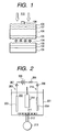
- the electrically conductive substrate 203 is used the above-described substrate 101 with a metal layer 102 formed thereon.
- the counter electrode 204 of the apparatus is a buffed zinc plate and used as an anode.
- the zinc content in the zinc plate is preferably 90% or more and more preferably 99% or more.
- microwave (MW) plasma CVD or high frequency (RF, VHF) CVD is suitably used.
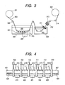
- the counter electrode 307 includes one or more square zinc plates of 99.99% purity.
- the DC power source 308 is controlled so that a voltage is applied across the substrate in a continuous length 303, as a cathode, and the counter electrode 307, as an anode, to keep current flow constant.
- the substrate strip 508 is, for example, a conductive substrate strip of stainless steel sheet 0.13 mm thick and 36 cm wide. While the substrate strip is being wound off from the feeding chamber 505, continuously conveyed to pass through 4 deposition chambers 504, 501, 502 and 503 and wound up into the wind-up chamber 506, an adsorption preventive layer and a three-layered nip (or pin) structure silicon non-single crystal semiconductor film for a photovoltaic device are formed on the surface of the substrate strip.
- the plasma treatment with a rare gas or nitrogen gas is carried out by plasma CVD, just as is done the semiconductor deposition; therefore, the treatment chamber is easy to place in the front portion of the semiconductor deposition apparatus.
- the treatment temperature is preferably the same as the temperature at which the doped layer adjacent to the zinc oxide layer is deposited and the treatment pressure is preferably 10 to 2,500 Pa.
- the making power is suitably in the range of 0.1 to 2.0 W, though it varies depending on the frequency of the high-frequency power source, the distance between the substrate and the cathode and the pressure in the chamber.
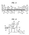
- a zinc oxide film was formed on a substrate in the same manner as in Example 1, and then the substrate 602 was introduced into a heat treatment chamber 601 shown in FIG. 6 and dehydrated for 10 minutes while increasing the temperature of the object to be treated (substrate) from room temperature up to 200°C in increments of 2.0°C/min and, after completing the temperature increase, controlling the same with a heater output system 606 so as to keep the object to be treated at 200°C.
- a heater output system 606 so as to keep the object to be treated at 200°C.
- each substrate was set in the substrate holder 425 and set on the rail 424 of the load chamber 401. Then the load chamber 401 was evacuated to a vacuum degree of several hundreds Pa or less.
Landscapes
- Chemical & Material Sciences (AREA)
- Inorganic Chemistry (AREA)
- Engineering & Computer Science (AREA)
- Chemical Kinetics & Catalysis (AREA)
- Electrochemistry (AREA)
- Materials Engineering (AREA)
- Metallurgy (AREA)
- Organic Chemistry (AREA)
- Photovoltaic Devices (AREA)
Applications Claiming Priority (4)
| Application Number | Priority Date | Filing Date | Title |
|---|---|---|---|
| JP2003085880 | 2003-03-26 | ||
| JP2003085880 | 2003-03-26 | ||
| JP2004066561A JP2004311965A (ja) | 2003-03-26 | 2004-03-10 | 光起電力素子の製造方法 |
| JP2004066561 | 2004-03-10 |
Publications (1)
| Publication Number | Publication Date |
|---|---|
| EP1463128A2 true EP1463128A2 (de) | 2004-09-29 |
Family
ID=32829045
Family Applications (1)
| Application Number | Title | Priority Date | Filing Date |
|---|---|---|---|
| EP04007128A Withdrawn EP1463128A2 (de) | 2003-03-26 | 2004-03-24 | Verfahren zur Herstellung einer photovoltaischen Vorrichtung |
Country Status (5)
| Country | Link |
|---|---|
| US (1) | US20040191950A1 (de) |
| EP (1) | EP1463128A2 (de) |
| JP (1) | JP2004311965A (de) |
| CN (1) | CN1534799A (de) |
| AU (1) | AU2004201229A1 (de) |
Cited By (1)
| Publication number | Priority date | Publication date | Assignee | Title |
|---|---|---|---|---|
| US10186619B2 (en) | 2009-11-20 | 2019-01-22 | Semiconductor Energy Laboratory Co., Ltd. | Method for manufacturing semiconductor device |
Families Citing this family (28)
| Publication number | Priority date | Publication date | Assignee | Title |
|---|---|---|---|---|
| JP2006269607A (ja) * | 2005-03-23 | 2006-10-05 | Canon Inc | 光起電力素子の製造方法 |
| JP5037808B2 (ja) | 2005-10-20 | 2012-10-03 | キヤノン株式会社 | アモルファス酸化物を用いた電界効果型トランジスタ、及び該トランジスタを用いた表示装置 |
| US20080308147A1 (en) * | 2007-06-12 | 2008-12-18 | Yiwei Lu | Rear electrode structure for use in photovoltaic device such as CIGS/CIS photovoltaic device and method of making same |
| US8071179B2 (en) | 2007-06-29 | 2011-12-06 | Stion Corporation | Methods for infusing one or more materials into nano-voids if nanoporous or nanostructured materials |
| US7687300B2 (en) * | 2007-10-22 | 2010-03-30 | Applied Materials, Inc. | Method of dynamic temperature control during microcrystalline SI growth |
| KR100870837B1 (ko) * | 2008-03-04 | 2008-11-28 | 한국철강 주식회사 | 산화아연 박막의 수분 제거 방법 |
| US8044594B2 (en) * | 2008-07-31 | 2011-10-25 | Advanced Energy Industries, Inc. | Power supply ignition system and method |
| US20100089318A1 (en) * | 2008-09-12 | 2010-04-15 | Ovshinsky Stanford R | Remote Plasma Apparatus for Manufacturing Solar Cells |
| US7947524B2 (en) | 2008-09-30 | 2011-05-24 | Stion Corporation | Humidity control and method for thin film photovoltaic materials |
| US8741689B2 (en) * | 2008-10-01 | 2014-06-03 | Stion Corporation | Thermal pre-treatment process for soda lime glass substrate for thin film photovoltaic materials |
| US20110018103A1 (en) * | 2008-10-02 | 2011-01-27 | Stion Corporation | System and method for transferring substrates in large scale processing of cigs and/or cis devices |
| US8395078B2 (en) * | 2008-12-05 | 2013-03-12 | Advanced Energy Industries, Inc | Arc recovery with over-voltage protection for plasma-chamber power supplies |
| EP2790205B1 (de) | 2009-02-17 | 2018-04-04 | Solvix GmbH | Stromversorgungsvorrichtung zur Plasmabearbeitung |
| US8241943B1 (en) | 2009-05-08 | 2012-08-14 | Stion Corporation | Sodium doping method and system for shaped CIGS/CIS based thin film solar cells |
| US8372684B1 (en) | 2009-05-14 | 2013-02-12 | Stion Corporation | Method and system for selenization in fabricating CIGS/CIS solar cells |
| US8507786B1 (en) | 2009-06-27 | 2013-08-13 | Stion Corporation | Manufacturing method for patterning CIGS/CIS solar cells |
| KR101460868B1 (ko) | 2009-07-10 | 2014-11-11 | 가부시키가이샤 한도오따이 에네루기 켄큐쇼 | 반도체 장치 |
| KR101127491B1 (ko) * | 2009-07-29 | 2012-03-23 | 삼성코닝정밀소재 주식회사 | 태양전지 기판 제조방법 |
| JP5224470B2 (ja) * | 2009-07-31 | 2013-07-03 | 国立大学法人東北大学 | 光電変換部材 |
| US8398772B1 (en) | 2009-08-18 | 2013-03-19 | Stion Corporation | Method and structure for processing thin film PV cells with improved temperature uniformity |
| US8859880B2 (en) * | 2010-01-22 | 2014-10-14 | Stion Corporation | Method and structure for tiling industrial thin-film solar devices |
| US9096930B2 (en) | 2010-03-29 | 2015-08-04 | Stion Corporation | Apparatus for manufacturing thin film photovoltaic devices |
| US8142521B2 (en) * | 2010-03-29 | 2012-03-27 | Stion Corporation | Large scale MOCVD system for thin film photovoltaic devices |
| US8361229B2 (en) * | 2010-04-22 | 2013-01-29 | Primestar Solar, Inc. | Seal configuration for a system for continuous deposition of a thin film layer on a substrate |
| US8461061B2 (en) | 2010-07-23 | 2013-06-11 | Stion Corporation | Quartz boat method and apparatus for thin film thermal treatment |
| US8552665B2 (en) | 2010-08-20 | 2013-10-08 | Advanced Energy Industries, Inc. | Proactive arc management of a plasma load |
| CN103173829A (zh) * | 2013-04-19 | 2013-06-26 | 济南大学 | 一种电化学沉积制备碲化镉半导体薄膜的方法 |
| CN114342090A (zh) * | 2019-08-30 | 2022-04-12 | 京浜乐梦金属科技株式会社 | 积层结构体及积层结构体的制造方法 |
Family Cites Families (21)
| Publication number | Priority date | Publication date | Assignee | Title |
|---|---|---|---|---|
| US5180434A (en) * | 1991-03-11 | 1993-01-19 | United Solar Systems Corporation | Interfacial plasma bars for photovoltaic deposition apparatus |
| US5769963A (en) * | 1995-08-31 | 1998-06-23 | Canon Kabushiki Kaisha | Photovoltaic device |
| DE69702277T2 (de) * | 1996-03-06 | 2001-03-01 | Canon K.K., Tokio/Tokyo | Verfahren zur Herstellung einer Dünnzinkoxidfilm und Verfahren zur Herstellung eines Substrats einer Halbleiteranordnung und Verfahren zur Herstellung einer photoelektrischen Umwandlungsvorrichtung unter Verwendung dieser Film |
| US6172296B1 (en) * | 1996-05-17 | 2001-01-09 | Canon Kabushiki Kaisha | Photovoltaic cell |
| US6123824A (en) * | 1996-12-13 | 2000-09-26 | Canon Kabushiki Kaisha | Process for producing photo-electricity generating device |
| JPH10335684A (ja) * | 1997-05-30 | 1998-12-18 | Canon Inc | 光電気変換体の製造方法 |
| JPH1146006A (ja) * | 1997-07-25 | 1999-02-16 | Canon Inc | 光起電力素子およびその製造方法 |
| JPH11233801A (ja) * | 1998-02-17 | 1999-08-27 | Canon Inc | 微結晶シリコン膜の形成方法、および光起電力素子 |
| JP4208281B2 (ja) * | 1998-02-26 | 2009-01-14 | キヤノン株式会社 | 積層型光起電力素子 |
| US6303945B1 (en) * | 1998-03-16 | 2001-10-16 | Canon Kabushiki Kaisha | Semiconductor element having microcrystalline semiconductor material |
| US6344608B2 (en) * | 1998-06-30 | 2002-02-05 | Canon Kabushiki Kaisha | Photovoltaic element |
| US6472248B2 (en) * | 1999-07-04 | 2002-10-29 | Canon Kabushiki Kaisha | Microcrystalline series photovoltaic element and process for fabrication of same |
| JP4171162B2 (ja) * | 2000-05-30 | 2008-10-22 | 三洋電機株式会社 | 光起電力素子およびその製造方法 |
| JP2002206168A (ja) * | 2000-10-24 | 2002-07-26 | Canon Inc | シリコン系薄膜の形成方法、シリコン系半導体層の形成方法及び光起電力素子 |
| JP2002134772A (ja) * | 2000-10-24 | 2002-05-10 | Canon Inc | シリコン系薄膜及び光起電力素子 |
| JP2002237606A (ja) * | 2000-12-04 | 2002-08-23 | Canon Inc | 太陽電池用基板、それを用いた太陽電池及び太陽電池の製造方法 |
| JP2002305315A (ja) * | 2001-01-31 | 2002-10-18 | Canon Inc | 半導体素子の形成方法及び半導体素子 |
| US6706336B2 (en) * | 2001-02-02 | 2004-03-16 | Canon Kabushiki Kaisha | Silicon-based film, formation method therefor and photovoltaic element |
| US6858308B2 (en) * | 2001-03-12 | 2005-02-22 | Canon Kabushiki Kaisha | Semiconductor element, and method of forming silicon-based film |
| JP2003007629A (ja) * | 2001-04-03 | 2003-01-10 | Canon Inc | シリコン系膜の形成方法、シリコン系膜および半導体素子 |
| JP2003046496A (ja) * | 2001-07-31 | 2003-02-14 | Canon Inc | 情報管理方法、情報管理システム及び処理装置 |
-
2004
- 2004-03-10 JP JP2004066561A patent/JP2004311965A/ja not_active Withdrawn
- 2004-03-23 US US10/806,157 patent/US20040191950A1/en not_active Abandoned
- 2004-03-24 AU AU2004201229A patent/AU2004201229A1/en not_active Abandoned
- 2004-03-24 EP EP04007128A patent/EP1463128A2/de not_active Withdrawn
- 2004-03-25 CN CNA2004100085877A patent/CN1534799A/zh active Pending
Cited By (1)
| Publication number | Priority date | Publication date | Assignee | Title |
|---|---|---|---|---|
| US10186619B2 (en) | 2009-11-20 | 2019-01-22 | Semiconductor Energy Laboratory Co., Ltd. | Method for manufacturing semiconductor device |
Also Published As
| Publication number | Publication date |
|---|---|
| CN1534799A (zh) | 2004-10-06 |
| JP2004311965A (ja) | 2004-11-04 |
| AU2004201229A1 (en) | 2004-10-14 |
| US20040191950A1 (en) | 2004-09-30 |
Similar Documents
| Publication | Publication Date | Title |
|---|---|---|
| EP1463128A2 (de) | Verfahren zur Herstellung einer photovoltaischen Vorrichtung | |
| US7282132B2 (en) | Zinc oxide film treatment method and method of manufacturing photovoltaic device utilizing the same | |
| EP0895291B1 (de) | Photovoltaisches Bauelement und Verfahren zu dessen Herstellung | |
| US6331672B1 (en) | Photovoltaic cell and method for manufacturing the same | |
| US6576112B2 (en) | Method of forming zinc oxide film and process for producing photovoltaic device using it | |
| EP1463126A2 (de) | Gestapeltes photovoltaisches Bauelement | |
| US6812499B2 (en) | Silicon-based film and photovoltaic element | |
| US7445952B2 (en) | Method of forming laminate and method of manufacturing photovoltaic device | |
| Takano et al. | Light-weight and large-area solar cell production technology | |
| US6653165B2 (en) | Methods of forming semiconductor element, and semiconductor elements | |
| KR101179443B1 (ko) | 박막 태양 전지를 대량 생산하기 위한 보호층 | |
| JP3027670B2 (ja) | 光起電力素子 | |
| US20030085129A1 (en) | Method of forming zinc oxide film, method of producing semiconductor element substrate using same, and method of producing photovoltaic element | |
| US20050150773A1 (en) | Method for forming deposition film and method for producing photovoltaic device | |
| JP2006269607A (ja) | 光起電力素子の製造方法 | |
| JP2000004036A (ja) | 微結晶半導体層の形成方法、および光起電力素子 | |
| JP2001358350A (ja) | 光起電力素子 | |
| JP2002134773A (ja) | 光起電力素子 | |
| JP4012106B2 (ja) | 光起電力素子形成方法 | |
| JP2713847B2 (ja) | 薄膜太陽電池 | |
| JPH0969640A (ja) | 光起電力素子 | |
| JPH11274540A (ja) | 光起電力素子及びその製造方法 | |
| JP3017421B2 (ja) | 光起電力素子 | |
| JP3072831B2 (ja) | 光起電力素子 | |
| JP2003158085A (ja) | 堆積膜形成方法 |
Legal Events
| Date | Code | Title | Description |
|---|---|---|---|
| PUAI | Public reference made under article 153(3) epc to a published international application that has entered the european phase |
Free format text: ORIGINAL CODE: 0009012 |
|
| AK | Designated contracting states |
Kind code of ref document: A2 Designated state(s): AT BE BG CH CY CZ DE DK EE ES FI FR GB GR HU IE IT LI LU MC NL PL PT RO SE SI SK TR |
|
| AX | Request for extension of the european patent |
Extension state: AL LT LV MK |
|
| STAA | Information on the status of an ep patent application or granted ep patent |
Free format text: STATUS: THE APPLICATION HAS BEEN WITHDRAWN |
|
| 18W | Application withdrawn |
Effective date: 20060713 |