EP1465200B1 - Statische Direktzugriffspeicherzelle (SRAM) und Speichereinheit die diese enthält mit extrem niedrigem Leistungsverbrauch - Google Patents
Statische Direktzugriffspeicherzelle (SRAM) und Speichereinheit die diese enthält mit extrem niedrigem Leistungsverbrauch Download PDFInfo
- Publication number
- EP1465200B1 EP1465200B1 EP04290885A EP04290885A EP1465200B1 EP 1465200 B1 EP1465200 B1 EP 1465200B1 EP 04290885 A EP04290885 A EP 04290885A EP 04290885 A EP04290885 A EP 04290885A EP 1465200 B1 EP1465200 B1 EP 1465200B1
- Authority
- EP
- European Patent Office
- Prior art keywords
- transistors
- memory cell
- bit line
- access
- charge
- Prior art date
- Legal status (The legal status is an assumption and is not a legal conclusion. Google has not performed a legal analysis and makes no representation as to the accuracy of the status listed.)
- Expired - Lifetime
Links
- 230000015654 memory Effects 0.000 title claims abstract description 64
- 230000003068 static effect Effects 0.000 title claims abstract description 9
- 230000000295 complement effect Effects 0.000 claims abstract description 18
- 239000000758 substrate Substances 0.000 claims abstract description 13
- 238000007667 floating Methods 0.000 claims abstract description 12
- 229910044991 metal oxide Inorganic materials 0.000 claims abstract description 3
- 150000004706 metal oxides Chemical class 0.000 claims abstract description 3
- 239000004065 semiconductor Substances 0.000 claims abstract description 3
- 238000005516 engineering process Methods 0.000 claims description 26
- 239000012212 insulator Substances 0.000 claims description 3
- XUIMIQQOPSSXEZ-UHFFFAOYSA-N Silicon Chemical compound [Si] XUIMIQQOPSSXEZ-UHFFFAOYSA-N 0.000 claims 1
- 230000006870 function Effects 0.000 description 13
- 238000003860 storage Methods 0.000 description 11
- 230000002123 temporal effect Effects 0.000 description 7
- 230000014759 maintenance of location Effects 0.000 description 6
- 230000008901 benefit Effects 0.000 description 5
- 230000010354 integration Effects 0.000 description 4
- 230000008878 coupling Effects 0.000 description 3
- 238000010168 coupling process Methods 0.000 description 3
- 238000005859 coupling reaction Methods 0.000 description 3
- 238000010586 diagram Methods 0.000 description 3
- 238000000034 method Methods 0.000 description 3
- 230000008569 process Effects 0.000 description 3
- 230000003213 activating effect Effects 0.000 description 2
- 238000012423 maintenance Methods 0.000 description 2
- 239000011159 matrix material Substances 0.000 description 2
- 230000004913 activation Effects 0.000 description 1
- 230000000903 blocking effect Effects 0.000 description 1
- 230000008094 contradictory effect Effects 0.000 description 1
- 238000005265 energy consumption Methods 0.000 description 1
- 230000036039 immunity Effects 0.000 description 1
- 230000006872 improvement Effects 0.000 description 1
- 238000004519 manufacturing process Methods 0.000 description 1
- 230000007246 mechanism Effects 0.000 description 1
- 230000000704 physical effect Effects 0.000 description 1
- 230000035945 sensitivity Effects 0.000 description 1
- 229910052710 silicon Inorganic materials 0.000 description 1
- 239000010703 silicon Substances 0.000 description 1
- 238000004513 sizing Methods 0.000 description 1
Images


Classifications
-
- H—ELECTRICITY
- H10—SEMICONDUCTOR DEVICES; ELECTRIC SOLID-STATE DEVICES NOT OTHERWISE PROVIDED FOR
- H10B—ELECTRONIC MEMORY DEVICES
- H10B10/00—Static random access memory [SRAM] devices
- H10B10/12—Static random access memory [SRAM] devices comprising a MOSFET load element
- H10B10/125—Static random access memory [SRAM] devices comprising a MOSFET load element the MOSFET being a thin film transistor [TFT]
-
- H—ELECTRICITY
- H10—SEMICONDUCTOR DEVICES; ELECTRIC SOLID-STATE DEVICES NOT OTHERWISE PROVIDED FOR
- H10B—ELECTRONIC MEMORY DEVICES
- H10B10/00—Static random access memory [SRAM] devices
Definitions
- the present invention relates to a static random access memory cell (SRAM) operating at ultra-low voltage for ultra-low power consumption. It also relates to an ultra low consumption memory unit made from such cells.
- SRAM static random access memory cell
- Memory cells of type 4T-2R already exist. These cells require a high cell ratio to provide stability and exhibit a high quiescent leakage current.
- 4T-2TFT type memory cells are compatible with CMOS technologies and their resistance modulated allows an improvement of the compromise between the idle current (Ioff) and the charge current of the cell (Ion).
- the 6T PMOS LOAD memory cells are compatible with CMOS technologies and their active pull-up structure ensures cell stability and good immunity to errors. These memory cells have a low leakage current at rest. However, writing in these cells is more difficult than in 4T-2R / TFT cells. In addition, their dimensions are larger than those of 4T-2R / TFT cells by a factor of 1.5 to 2.
- memory cells with new architectures such as the HITACHI source-line control cell architecture
- HITACHI source-line control cell architecture has been developed and disclosed in the article entitled “Driving Source-Line Cell Architecture for High-Speed Low-Power Applications Sub-1V” published in the journal “IEEE Journal Solid-State Circuits” Vol. 31, No. 4, April 1996 .
- This cell architecture which is suitable for low voltage applications and therefore low power, requires the generation of additional signals and in particular a negative voltage source.
- SL Vss, while in read, SL ⁇ 0, and write, SL is floating.
- CMOS 4T cell architecture proposed by NEC and disclosed in the article entitled “A 16-Mb 400-MHz Loadless CMOS Four-Transistor SRAM Macro” published in the journal “IEEE Journal of Solid-State Circuits” Vol.35, No.11, November 2000 .
- This cell is in practice the size of a 4T-2R type cell. However, it is sensitive to the mismatch of technology and temperature. Moreover, it requires circuits additional features to provide the cell refresh function and its reliability.
- CMOS 4T cell architectures with no conduction transistors patented by Texas Instrument (TI) and Monolithic System Technology (Mosys) in 2002, titled “Loadless 4T SRAM cell with PMOS drivers” and "High-density ratio- independent four-transistor RAM cell fabricated with conventional logic process and respective reference NO. US 2002/0051379 A1 and No. US 6,442,060 B1 .
- the architectures proposed in these two patents have been developed in CMOS BULK technology. Compared with the NEC architecture, the latter have the advantage of a better temperature stability due to the gate current of the PMOS type transistors, which are ten times smaller than those of the NMOS transistors.
- the cell TI has the disadvantage, in read mode, of activating the access transistors with a voltage on the word line equal to 90% of the supply voltage of the device to guarantee good stability of the device. memory cell in this state. This constraint limits the conduction current leaving the cell during a read cycle and affects the performance of the system.
- the IT architecture is sensitive to the mismatching of the technology.
- the Mosys architecture it also has the advantage of having a very high integration rate due to the minimum dimensioning of the transistors of the cell. The counterpart relates to the need for a substrate supply of the PMOS load transistors higher than the supply voltage of the device to increase their threshold voltage and reduce their leakage currents.
- the static memory cell of the invention is defined by claim 1.
- the purpose of the present invention is to propose an ultra-low power memory cell topology, which makes it possible to remedy the aforementioned drawbacks.
- the load and access transistors are made in silicon-on-insulator (SOI) technology.
- the load transistors have the function of ensuring and maintaining the load necessary for the establishment of a logic level '1', corresponding to the equal potential. at the supply voltage, to one or other of the nodes according to the stored logic value.
- the two access transistors whose substrates are left floating, have the function of authorizing, during a read or write cycle, access to the node potentials. Moreover, these access transistors contribute to maintaining the logic level '0' at the nodes as a function of the stored logic value. The maintenance of the logical level '0' is carried out by a system of self-regulation of the loads of the node.
- the charge transistors are of the PMOS type and have their respective sources connected to a source of supply voltage, whereas the access transistors are of the NMOS type and have their respective drains connected respectively to the first and second storage nodes.
- the first and second load transistors (T L1 , T L2 ) have their respective drains respectively defining said first and second storage nodes and respectively connected to respective gates of the second load transistor and the first transistor.
- the first and second access transistors (T A1 , T A2 ) have their respective sources respectively connected to the bit line (BLT) and the complementary bit line (BLC).
- the first and second charge transistors are preferably mounted using dynamic threshold metal oxide semiconductor (DTMOS ) technology.
- DTMOS dynamic threshold metal oxide semiconductor
- the electrical charges, at one or the other of the storage nodes (A, B) according to the state of the bit line (BLT), are self-regulating so that the potential of said node is maintained at logic level 0 .
- the load transistors (T L1 , T L2 ) operate as PMOS type PMOS-type conduction transistors and the access transistors (T A1 , T A2 ) are of NMOS type and floating substrate.
- bit line (BLT) and the complementary bit line (BLC) are then preloaded to the supply voltage (V SS ), and the word line (WL) is provided to control the access transistors (T A1 , T A2 ), either in blocking at 0 volts, or in activation at the supply voltage (V DD ).
- a memory cell according to the invention makes it possible to precharge the bit lines to 0 and does not require a large potential difference between these bit lines during a write or read operation, which contributes to minimizing the power consumption of the bit lines of the memory cell.
- the present invention provides both a very good stability, a very low consumption and a high integration rate.
- the memory cell according to the invention is designed to operate at ultra low voltage, i.e. equal to or less than the conduction voltage of a PN junction (0.7 V and below).
- the ratio of the width of an access transistor to the width of the load transistor connected to the access transistor is preferably equal to or greater than 1.5 depending on the technology used.
- This memory unit is characterized in that the load and access transistors are made in Silicon on Insulator (SOI) technology, these load transistors being of PMOS type and having their respective sources connected to a source of supply voltage, and said access transistors being of NMOS type and having their respective drains respectively connected to said first and second storage nodes.
- SOI Silicon on Insulator
- the reading means of each memory cell may be arranged to operate either in voltage or in current.
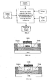
- a memory unit comprises, with reference to the figure 1 , an array of ultra-low power memory cells according to the invention, which are associated with an address register, a data input register, a clock, a write / read circuitry, and a data output register .
- the memory cells of the array which do not require a refresh cycle and have a very strong integration, are arranged in the form of a conventional matrix.
- the address register is intended to address or select a cell of the matrix. Its function is to decode the coordinates, that is to say the row and the column, of each cell from an address word of several bits.
- the function of the data input register is to provide the bits of a word that must be stored in the table during a write operation.
- the function of the data output register is to receive the bits of the stored word at the address defined in the address register during a read operation.
- the access transistors provided in a memory cell according to the invention have, with reference to the figure 2a , a floating substrate NMOS / SOI transistor structure, while the load transistors have, with reference to the figure 2b , a PMOS / SOI transistor structure mounted in DTMOS.
- Each memory cell includes, in the diagram of the figure 3 , two load transistors T L1 , T L2 PMOS / SOI type mounted in DTMOS, whose function is to ensure and maintain the load required to establish a logic level '1' corresponding to a potential equal to the supply voltage V dd .
- the respective sources of these two load transistors are connected to a line maintained at this supply voltage V dd , while their respective drains are connected to the respective gates of the opposite transistors and represent the two storage nodes A, B.
- Each memory cell further comprises two access transistors T A1 , T A2 whose function is to allow, during a read or write cycle, access to the potentials of the nodes A and B. Moreover, these two access transistors contribute, in retention mode, to maintain the logic level '0' at the nodes A or B as a function of the stored logic value. The maintenance of the logic level '0' is obtained by a self-regulating mechanism of the loads of the node which will be explained in the following.
- the respective drains of the two access transistors T A1 , T A2 are connected, at the nodes A and B, to the respective drains of the two load transistors, while their respective sources are respectively connected to a bit line BLT and to a line complementary bit BLC.
- the respective gates of the two access transistors T A1 , T A2 are connected to a word line WL.
- the new memory cell topology according to the invention offers the advantage of not requiring a refresh cycle and ensuring, thanks to a strong feedback between the two load transistors.
- T L1 , T L2 good logical levels.
- the word line WL and the bit lines BLT, BLC are polarized and held at zero potential.
- the access transistors T A1 , T A2 then have Grid-Source voltages V 0 equal to 0V, which conditions them in a blocked state. Drain-source currents, derived from these transistors, are leakage currents proportional to the V -source and V- drain-source voltages of each of them.
- the access transistor T A2 To maintain the potential of the node B close to 0V, it is necessary for the access transistor T A2 to conduct the current from the charge transistor T L2 in the complementary bit line BLC.
- the leakage current driven by the access transistor T A2 is a function of the potential of its floating substrate (body). If the potential V (B) at the node B increases, the potential of the floating substrate of the access transistor T A2 also increases by physical effects specific to the SOI technology and by a capacitive coupling C drain-body which exists between the drain and the floating substrate of the transistor. This results in an exponential increase of the current in the access transistor T A2 which rapidly becomes larger than the current supplied by the load transistor T L2 , thus limiting the load of the node B. At the same time, the decrease of the Voltage V Drain-Source of the charge transistor T L2 and the increase of the voltage V Drain-Source of the access transistor T A2 reinforce this evolution (decrease and linear increase of the current according to VDS).
- FIG 4 which represents the stability of a memory cell according to the invention by the variation of the voltage difference (V (A) -V (B)) between the node A and the node B as a function of the ratio r, it appears that the memory cell is stable as long as the voltage difference is positive.
- the stability study of a memory cell according to the invention was carried out in standard or typical operation and in limiting situations, in particular in the presence of process noise (in English: mismatch) between the transistors and in the presence of temperature.
- process noise in English: mismatch
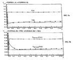
- the potential V (B) at the node B of a memory cell according to the invention tends towards a value of constant potential and of low amplitude, according to a self-regulation process of the potential of the node B.
- the dynamic charge of the floating substrate of the access transistors T A1 , T A2 via a Grille-Body capacitive coupling when switching the signal WL on the word line ( figure 6a ), as well as a very strong feedback of the load transistors T L1 , T L2 mounted in DTMOS, contribute to increasing the writing speed of the memory cells according to the invention which is intrinsically moderate because of a low supply voltage (of the order of half a volt and below). It should be noted that the maximum operating voltage is limited only by the conduction voltage of a PN junction, generally 0.6V.
- bit lines BLT and BLC are loaded in a complementary manner. If it is desired to write a logical '0' to node B and a logic '1' to node A, the bit line BLT and the complementary bit line BLC are respectively loaded to a potential corresponding to the logic high level and a zero potential which tends to half of the supply voltage V dd .
- the word line WL is turned on and off a few nanoseconds after and before the bit lines are themselves turned on and off.
- the Figures 6a to 6e illustrate a write cycle and highlight the dynamic loading of floating substrates of access transistors ( figure 6e ) as well as the feedback phenomenon of the load transistors ( figure 6d ).
- the very good feedback of the memory cell structure according to the invention is due to a very good ratio I on (current passing) / I off (leakage current in blocked mode) of the load transistors T L1 , T L2 mounted in DTMOS .
- the reading mode of a memory cell according to the invention can be achieved either in voltage or in current.
- Grid-Body capacitive coupling of the access transistors contributes to dynamically charging their substrate and boosting their ability to conduct current. Thanks to the very good I on / I off ratio of the load transistors T L1 , T L2 , the ratio of the current I drain-source of the first access transistor T A1 to the current I drain-source of the second access transistor T A2 is also very high, which gives a great advantage for a reading current.
Landscapes
- Semiconductor Memories (AREA)
- Static Random-Access Memory (AREA)
Claims (4)
- SRAM genannte statische Direktzugriffspeicherzelle, umfassend:- einen ersten und einen zweiten Ladungstransistor (TL1, TL2) der MOSFET-Technologie, die angeordnet sind, um die jeweiligen Potentiale eines ersten und eines zweiten Spelcherknotenpunkts (A, B) Im Verhältnis zu einer Spannungsreferenz zu steuern und halten, und- einen ersten und einen zweiten Zugriffstransistor (TA1, TA2), die In einer MOSFET-Technologle, die zu der der besagten Ladungstransistoren ergänzend ist, und die jeweils (i) zwischen einer Bitleitung (BLT) und dem besagten ersten Speicherknotenpunkt (A), und (ii) zwischen einer ergänzenden Bitleitung (BLC) und dem besagten zweiten Speicherknotenpunkt (B) angeordnet sind, wobei die Gates dieser Zugriffstransistoren jeweils mit einer Wortleitung (WL) verbunden sind,- wobei die jeweilige Drain-Anschlüsse des ersten und des zweiten Ladungstransistors (TL1, TL2) jeweils den besagten ersten und zweiten Speicherknotenpunkt definieren und jeweils mit den jeweiligen Gates des besagten zweiten Ladungstransistors und des besagten ersten Ladungstransistors verbunden sind, und die jeweilige Source-Anschlüsse des ersten und des zweiten Zugriffstransistors (TA1, TA2), jeweils mit der Bitleitung (BLT) und der ergänzenden Bitleitung (BLC) verbunden sind,- wobei die Ladungstransistoren (TL1, TL2) vom PMOS-Typ sind und ihre jeweiligen Source-Anschlüsse mit einer Versorgungsspannungsquelle (VDD) verbunden sind, und dabei die Zugriffstransistoren (TA1, TA2) vom NMOS-Typ sind und ihre jeweiligen Drain-Anschlüsse jeweils mit dem besagten ersten und zweiten Speicherknotenpunkt (A, B) verbunden sind,dadurch gekennzeichnet, dass:- die besagten Ladungstransistoren und die besagten Zugriffstransistoren in SOI genannte Silizium-auf-Isolator Technologie ausgebildet sind,- der erste und der zweite Ladungstransistor (TL1, TL2) gemäß der DTMOS-Konfiguration montiert werden, die Dynamic Threshold Metal Oxide Semiconductor oder Metaloxidhalbleiter mit dynamischer Schwelle genannt ist, und,- der erste und der zweite Zugriffstransistor (TA1, TA2) vom mit Schwimmsubstrat sind.
- Spelcherzelle gemäß Anspruch 1, dadurch gekennzeichnet, dass die Bitleitung (BLT) und die ergänzende Bitleitung (BLC) auf 0 V vorgeladen werden, und dass die Wortleitung (WL) dazu vorgesehen ist, die Zugriffstransistoren (TA1, TA2) zu steuern.
- Speicherzelle gemäß den Ansprüchen 1 und 2, dadurch gekennzeichnet, dass die Versorgungsspannungsquelle (VDD) gleich oder kleiner als die Leitungsspannung der PN-Übergänge der Transistoren der verwendeten Technologie ist.
- Speicherzelle, die ein Array von SRAM genannten statischen Direktzugriffspeicherzellen gemäß Anspruch 1 umfasst, dadurch gekennzeichnet, dass sle außerdem Registermittel für den Dateneingang, Registermittel für den Datenausgang, Registermittel für die Adresse und Schreib- /Lesemittel umfasst.
Applications Claiming Priority (2)
| Application Number | Priority Date | Filing Date | Title |
|---|---|---|---|
| FR0304127A FR2853445B1 (fr) | 2003-04-02 | 2003-04-02 | Cellule memoire statique a acces aleatoire(sram), et unite memoire a ultra basse consommation realisee a partir de telles cellules |
| FR0304127 | 2003-04-02 |
Publications (2)
| Publication Number | Publication Date |
|---|---|
| EP1465200A1 EP1465200A1 (de) | 2004-10-06 |
| EP1465200B1 true EP1465200B1 (de) | 2008-11-12 |
Family
ID=32843132
Family Applications (1)
| Application Number | Title | Priority Date | Filing Date |
|---|---|---|---|
| EP04290885A Expired - Lifetime EP1465200B1 (de) | 2003-04-02 | 2004-04-02 | Statische Direktzugriffspeicherzelle (SRAM) und Speichereinheit die diese enthält mit extrem niedrigem Leistungsverbrauch |
Country Status (4)
| Country | Link |
|---|---|
| EP (1) | EP1465200B1 (de) |
| AT (1) | ATE414318T1 (de) |
| DE (1) | DE602004017664D1 (de) |
| FR (1) | FR2853445B1 (de) |
Families Citing this family (8)
| Publication number | Priority date | Publication date | Assignee | Title |
|---|---|---|---|---|
| FR2898432B1 (fr) | 2006-03-10 | 2008-04-11 | Commissariat Energie Atomique | Cellules memoire en technologie cmos double-grille dotee de transistors a deux grilles independantes |
| FR2910999B1 (fr) | 2006-12-28 | 2009-04-03 | Commissariat Energie Atomique | Cellule memoire dotee de transistors double-grille, a grilles independantes et asymetriques |
| FR2911004B1 (fr) | 2006-12-28 | 2009-05-15 | Commissariat Energie Atomique | Procede de realisation de transistors a double-grille asymetriques permettant la realisation de transistors a double-grille asymetriques et symetriques sur un meme substrat |
| US7995251B2 (en) | 2007-03-30 | 2011-08-09 | Ricoh Company, Limited | Optical scanning device, optical scanning method, and image forming apparatus |
| FR2921508A1 (fr) | 2007-09-24 | 2009-03-27 | Commissariat Energie Atomique | Memoire sram a cellule de reference de polarisation |
| TWI423258B (zh) * | 2009-02-13 | 2014-01-11 | 寫入操作時提高寫入用字元線電壓位準之雙埠靜態隨機存取記憶體 | |
| US8213219B2 (en) * | 2009-07-29 | 2012-07-03 | GlobalFoundries, Inc. | Transistor-based memory cell and related operating methods |
| FR2958077B1 (fr) * | 2010-03-26 | 2013-11-15 | Commissariat Energie Atomique | Cellule memoire sram a quatre transistors munis d'une contre-electrode |
Family Cites Families (5)
| Publication number | Priority date | Publication date | Assignee | Title |
|---|---|---|---|---|
| US5943258A (en) * | 1997-12-24 | 1999-08-24 | Texas Instruments Incorporated | Memory with storage cells having SOI drive and access transistors with tied floating body connections |
| US6442060B1 (en) * | 2000-05-09 | 2002-08-27 | Monolithic System Technology, Inc. | High-density ratio-independent four-transistor RAM cell fabricated with a conventional logic process |
| US6731533B2 (en) * | 2000-10-31 | 2004-05-04 | Texas Instruments Incorporated | Loadless 4T SRAM cell with PMOS drivers |
| US20020112137A1 (en) * | 2000-12-31 | 2002-08-15 | Texas Instruments Incorporated | Partial trench body ties in sram cell |
| JP2002246600A (ja) * | 2001-02-13 | 2002-08-30 | Mitsubishi Electric Corp | 半導体装置及びその製造方法 |
-
2003
- 2003-04-02 FR FR0304127A patent/FR2853445B1/fr not_active Expired - Fee Related
-
2004
- 2004-04-02 DE DE602004017664T patent/DE602004017664D1/de not_active Expired - Lifetime
- 2004-04-02 EP EP04290885A patent/EP1465200B1/de not_active Expired - Lifetime
- 2004-04-02 AT AT04290885T patent/ATE414318T1/de not_active IP Right Cessation
Also Published As
| Publication number | Publication date |
|---|---|
| FR2853445B1 (fr) | 2005-10-14 |
| FR2853445A1 (fr) | 2004-10-08 |
| ATE414318T1 (de) | 2008-11-15 |
| DE602004017664D1 (de) | 2008-12-24 |
| EP1465200A1 (de) | 2004-10-06 |
Similar Documents
| Publication | Publication Date | Title |
|---|---|---|
| JP5822914B2 (ja) | 高性能スタティックメモリのリテイン・ティル・アクセスド(rta)省電力モード | |
| EP1833090B1 (de) | Speicherzellen der CMOS-Technologie mit Doppel-Gate, die mit Transistoren mit zwei unabhängigen Gates ausgestattet sind | |
| EP3217407B1 (de) | Sram-speicherzelle mit n-tfet und p-tfet | |
| US7742326B2 (en) | 8T SRAM cell with higher voltage on the read WL | |
| US6603345B2 (en) | Semiconductor device with reduced leakage of current | |
| US20110199837A1 (en) | High Voltage Word Line Driver | |
| JPH08235858A (ja) | 低電力及び低スレッショルドのcmosパストランジスタを使用し、漏れ電流を低減させた記憶セル | |
| FR2910999A1 (fr) | Cellule memoire dotee de transistors double-grille, a grilles independantes et asymetriques | |
| EP3010022B1 (de) | Speicherzelle mit lese-transistoren vom typ tfet und mosfet | |
| EP3002788B1 (de) | Vorrichtung mit sram-speicherzellen die mitteln zur polarisierung der wannen der speicherzelltransistoren umfasst | |
| FR2957449A1 (fr) | Micro-amplificateur de lecture pour memoire | |
| EP2040264B1 (de) | S-RAM-Speicher mit magnetischer Vergleichszelle | |
| EP3373303A1 (de) | Tfet-speicherlatch ohne aktualisierung | |
| EP1465200A1 (de) | Statische Direktzugriffspeicherzelle (SRAM) und Speichereinheit die diese enthält mit extrem niedrigem Leistungsverbrauch | |
| US20080031037A1 (en) | Semiconductor Memory Device | |
| FR2986652A1 (fr) | Memoire volatile a consommation reduite et capacite de stockage amelioree | |
| EP2003650B1 (de) | Asymmetrische SRAM-Speicherzelle mit 4 Doppelgate-Transistoren | |
| FR2878068A1 (fr) | Memoire a cellule de memorisation polarisee par groupe | |
| FR3130449A1 (fr) | Dispositif de pilotage de transistors et procédé de pilotage | |
| JP4075090B2 (ja) | 半導体装置 | |
| EP1103979A1 (de) | Dynamische Speicheranordnung mit wahlfreiem Zugriff (DRAM) sowie entsprechendes Leseverfahren | |
| FR3027442A1 (fr) | Cellule memoire a transistors tfet de memorisation polarises en inverse | |
| EP0910094B1 (de) | Dynamische Speicheranordnung mit verkürzter Auffrischungszeit und entsprechende Auffrischungsverfahren | |
| EP0910093A1 (de) | Dynamische Speicheranordnung | |
| FR2793341A1 (fr) | Memoire statique a quatre transistors desequilibres au niveau de leur courant de fuite et procede de commande d'une telle memoire |
Legal Events
| Date | Code | Title | Description |
|---|---|---|---|
| PUAI | Public reference made under article 153(3) epc to a published international application that has entered the european phase |
Free format text: ORIGINAL CODE: 0009012 |
|
| AK | Designated contracting states |
Kind code of ref document: A1 Designated state(s): AT BE BG CH CY CZ DE DK EE ES FI FR GB GR HU IE IT LI LU MC NL PL PT RO SE SI SK TR |
|
| AX | Request for extension of the european patent |
Extension state: AL HR LT LV MK |
|
| AKX | Designation fees paid | ||
| REG | Reference to a national code |
Ref country code: DE Ref legal event code: 8566 |
|
| 17P | Request for examination filed |
Effective date: 20050617 |
|
| RBV | Designated contracting states (corrected) |
Designated state(s): AT BE BG CH CY CZ DE DK EE ES FI FR GB GR HU IE IT LI LU MC NL PL PT RO SE SI SK TR |
|
| RAP1 | Party data changed (applicant data changed or rights of an application transferred) |
Owner name: COMMISSARIAT A L'ENERGIE ATOMIQUE ( CEA) |
|
| RIN1 | Information on inventor provided before grant (corrected) |
Inventor name: AMARA, AMARA Inventor name: THOMAS, OLIVIER |
|
| 17Q | First examination report despatched |
Effective date: 20070814 |
|
| GRAP | Despatch of communication of intention to grant a patent |
Free format text: ORIGINAL CODE: EPIDOSNIGR1 |
|
| GRAS | Grant fee paid |
Free format text: ORIGINAL CODE: EPIDOSNIGR3 |
|
| GRAA | (expected) grant |
Free format text: ORIGINAL CODE: 0009210 |
|
| AK | Designated contracting states |
Kind code of ref document: B1 Designated state(s): AT BE BG CH CY CZ DE DK EE ES FI FR GB GR HU IE IT LI LU MC NL PL PT RO SE SI SK TR |
|
| REG | Reference to a national code |
Ref country code: GB Ref legal event code: FG4D Free format text: NOT ENGLISH |
|
| REG | Reference to a national code |
Ref country code: CH Ref legal event code: EP |
|
| REG | Reference to a national code |
Ref country code: IE Ref legal event code: FG4D Free format text: LANGUAGE OF EP DOCUMENT: FRENCH |
|
| REF | Corresponds to: |
Ref document number: 602004017664 Country of ref document: DE Date of ref document: 20081224 Kind code of ref document: P |
|
| PG25 | Lapsed in a contracting state [announced via postgrant information from national office to epo] |
Ref country code: ES Free format text: LAPSE BECAUSE OF FAILURE TO SUBMIT A TRANSLATION OF THE DESCRIPTION OR TO PAY THE FEE WITHIN THE PRESCRIBED TIME-LIMIT Effective date: 20090223 Ref country code: AT Free format text: LAPSE BECAUSE OF FAILURE TO SUBMIT A TRANSLATION OF THE DESCRIPTION OR TO PAY THE FEE WITHIN THE PRESCRIBED TIME-LIMIT Effective date: 20081112 |
|
| NLV1 | Nl: lapsed or annulled due to failure to fulfill the requirements of art. 29p and 29m of the patents act | ||
| PG25 | Lapsed in a contracting state [announced via postgrant information from national office to epo] |
Ref country code: PL Free format text: LAPSE BECAUSE OF FAILURE TO SUBMIT A TRANSLATION OF THE DESCRIPTION OR TO PAY THE FEE WITHIN THE PRESCRIBED TIME-LIMIT Effective date: 20081112 Ref country code: NL Free format text: LAPSE BECAUSE OF FAILURE TO SUBMIT A TRANSLATION OF THE DESCRIPTION OR TO PAY THE FEE WITHIN THE PRESCRIBED TIME-LIMIT Effective date: 20081112 Ref country code: SI Free format text: LAPSE BECAUSE OF FAILURE TO SUBMIT A TRANSLATION OF THE DESCRIPTION OR TO PAY THE FEE WITHIN THE PRESCRIBED TIME-LIMIT Effective date: 20081112 Ref country code: FI Free format text: LAPSE BECAUSE OF FAILURE TO SUBMIT A TRANSLATION OF THE DESCRIPTION OR TO PAY THE FEE WITHIN THE PRESCRIBED TIME-LIMIT Effective date: 20081112 |
|
| REG | Reference to a national code |
Ref country code: IE Ref legal event code: FD4D |
|
| PG25 | Lapsed in a contracting state [announced via postgrant information from national office to epo] |
Ref country code: DK Free format text: LAPSE BECAUSE OF FAILURE TO SUBMIT A TRANSLATION OF THE DESCRIPTION OR TO PAY THE FEE WITHIN THE PRESCRIBED TIME-LIMIT Effective date: 20081112 Ref country code: BG Free format text: LAPSE BECAUSE OF FAILURE TO SUBMIT A TRANSLATION OF THE DESCRIPTION OR TO PAY THE FEE WITHIN THE PRESCRIBED TIME-LIMIT Effective date: 20090212 Ref country code: RO Free format text: LAPSE BECAUSE OF FAILURE TO SUBMIT A TRANSLATION OF THE DESCRIPTION OR TO PAY THE FEE WITHIN THE PRESCRIBED TIME-LIMIT Effective date: 20081112 Ref country code: EE Free format text: LAPSE BECAUSE OF FAILURE TO SUBMIT A TRANSLATION OF THE DESCRIPTION OR TO PAY THE FEE WITHIN THE PRESCRIBED TIME-LIMIT Effective date: 20081112 Ref country code: IE Free format text: LAPSE BECAUSE OF FAILURE TO SUBMIT A TRANSLATION OF THE DESCRIPTION OR TO PAY THE FEE WITHIN THE PRESCRIBED TIME-LIMIT Effective date: 20081112 |
|
| PG25 | Lapsed in a contracting state [announced via postgrant information from national office to epo] |
Ref country code: PT Free format text: LAPSE BECAUSE OF FAILURE TO SUBMIT A TRANSLATION OF THE DESCRIPTION OR TO PAY THE FEE WITHIN THE PRESCRIBED TIME-LIMIT Effective date: 20090413 Ref country code: SE Free format text: LAPSE BECAUSE OF FAILURE TO SUBMIT A TRANSLATION OF THE DESCRIPTION OR TO PAY THE FEE WITHIN THE PRESCRIBED TIME-LIMIT Effective date: 20090212 Ref country code: CZ Free format text: LAPSE BECAUSE OF FAILURE TO SUBMIT A TRANSLATION OF THE DESCRIPTION OR TO PAY THE FEE WITHIN THE PRESCRIBED TIME-LIMIT Effective date: 20081112 |
|
| PLBE | No opposition filed within time limit |
Free format text: ORIGINAL CODE: 0009261 |
|
| STAA | Information on the status of an ep patent application or granted ep patent |
Free format text: STATUS: NO OPPOSITION FILED WITHIN TIME LIMIT |
|
| PG25 | Lapsed in a contracting state [announced via postgrant information from national office to epo] |
Ref country code: SK Free format text: LAPSE BECAUSE OF FAILURE TO SUBMIT A TRANSLATION OF THE DESCRIPTION OR TO PAY THE FEE WITHIN THE PRESCRIBED TIME-LIMIT Effective date: 20081112 |
|
| 26N | No opposition filed |
Effective date: 20090813 |
|
| BERE | Be: lapsed |
Owner name: COMMISSARIAT A L'ENERGIE ATOMIQUE ( CEA) Effective date: 20090430 |
|
| REG | Reference to a national code |
Ref country code: CH Ref legal event code: PL |
|
| REG | Reference to a national code |
Ref country code: FR Ref legal event code: ST Effective date: 20091231 |
|
| PG25 | Lapsed in a contracting state [announced via postgrant information from national office to epo] |
Ref country code: LI Free format text: LAPSE BECAUSE OF NON-PAYMENT OF DUE FEES Effective date: 20090430 Ref country code: CH Free format text: LAPSE BECAUSE OF NON-PAYMENT OF DUE FEES Effective date: 20090430 |
|
| PG25 | Lapsed in a contracting state [announced via postgrant information from national office to epo] |
Ref country code: MC Free format text: LAPSE BECAUSE OF NON-PAYMENT OF DUE FEES Effective date: 20090430 Ref country code: FR Free format text: LAPSE BECAUSE OF NON-PAYMENT OF DUE FEES Effective date: 20091222 |
|
| PG25 | Lapsed in a contracting state [announced via postgrant information from national office to epo] |
Ref country code: BE Free format text: LAPSE BECAUSE OF NON-PAYMENT OF DUE FEES Effective date: 20090430 |
|
| PG25 | Lapsed in a contracting state [announced via postgrant information from national office to epo] |
Ref country code: GR Free format text: LAPSE BECAUSE OF FAILURE TO SUBMIT A TRANSLATION OF THE DESCRIPTION OR TO PAY THE FEE WITHIN THE PRESCRIBED TIME-LIMIT Effective date: 20090213 |
|
| PG25 | Lapsed in a contracting state [announced via postgrant information from national office to epo] |
Ref country code: LU Free format text: LAPSE BECAUSE OF NON-PAYMENT OF DUE FEES Effective date: 20090402 |
|
| PG25 | Lapsed in a contracting state [announced via postgrant information from national office to epo] |
Ref country code: HU Free format text: LAPSE BECAUSE OF FAILURE TO SUBMIT A TRANSLATION OF THE DESCRIPTION OR TO PAY THE FEE WITHIN THE PRESCRIBED TIME-LIMIT Effective date: 20090513 |
|
| PG25 | Lapsed in a contracting state [announced via postgrant information from national office to epo] |
Ref country code: TR Free format text: LAPSE BECAUSE OF FAILURE TO SUBMIT A TRANSLATION OF THE DESCRIPTION OR TO PAY THE FEE WITHIN THE PRESCRIBED TIME-LIMIT Effective date: 20081112 |
|
| PG25 | Lapsed in a contracting state [announced via postgrant information from national office to epo] |
Ref country code: CY Free format text: LAPSE BECAUSE OF FAILURE TO SUBMIT A TRANSLATION OF THE DESCRIPTION OR TO PAY THE FEE WITHIN THE PRESCRIBED TIME-LIMIT Effective date: 20081112 |
|
| PGFP | Annual fee paid to national office [announced via postgrant information from national office to epo] |
Ref country code: DE Payment date: 20120628 Year of fee payment: 9 |
|
| PGFP | Annual fee paid to national office [announced via postgrant information from national office to epo] |
Ref country code: GB Payment date: 20120425 Year of fee payment: 9 |
|
| PGFP | Annual fee paid to national office [announced via postgrant information from national office to epo] |
Ref country code: IT Payment date: 20120420 Year of fee payment: 9 |
|
| GBPC | Gb: european patent ceased through non-payment of renewal fee |
Effective date: 20130402 |
|
| PG25 | Lapsed in a contracting state [announced via postgrant information from national office to epo] |
Ref country code: DE Free format text: LAPSE BECAUSE OF NON-PAYMENT OF DUE FEES Effective date: 20131101 Ref country code: GB Free format text: LAPSE BECAUSE OF NON-PAYMENT OF DUE FEES Effective date: 20130402 |
|
| REG | Reference to a national code |
Ref country code: DE Ref legal event code: R119 Ref document number: 602004017664 Country of ref document: DE Effective date: 20131101 |
|
| PG25 | Lapsed in a contracting state [announced via postgrant information from national office to epo] |
Ref country code: IT Free format text: LAPSE BECAUSE OF NON-PAYMENT OF DUE FEES Effective date: 20130402 |