EP1469569A2 - Diode laser à semi-conducteur et assemblage comportant une telle diode - Google Patents
Diode laser à semi-conducteur et assemblage comportant une telle diode Download PDFInfo
- Publication number
- EP1469569A2 EP1469569A2 EP03258213A EP03258213A EP1469569A2 EP 1469569 A2 EP1469569 A2 EP 1469569A2 EP 03258213 A EP03258213 A EP 03258213A EP 03258213 A EP03258213 A EP 03258213A EP 1469569 A2 EP1469569 A2 EP 1469569A2
- Authority
- EP
- European Patent Office
- Prior art keywords
- semiconductor laser
- laser diode
- layer
- ridge waveguide
- protrusion
- Prior art date
- Legal status (The legal status is an assumption and is not a legal conclusion. Google has not performed a legal analysis and makes no representation as to the accuracy of the status listed.)
- Granted
Links
Images




Classifications
-
- H—ELECTRICITY
- H01—ELECTRIC ELEMENTS
- H01S—DEVICES USING THE PROCESS OF LIGHT AMPLIFICATION BY STIMULATED EMISSION OF RADIATION [LASER] TO AMPLIFY OR GENERATE LIGHT; DEVICES USING STIMULATED EMISSION OF ELECTROMAGNETIC RADIATION IN WAVE RANGES OTHER THAN OPTICAL
- H01S5/00—Semiconductor lasers
- H01S5/30—Structure or shape of the active region; Materials used for the active region
- H01S5/32—Structure or shape of the active region; Materials used for the active region comprising PN junctions, e.g. hetero- or double- heterostructures
- H01S5/323—Structure or shape of the active region; Materials used for the active region comprising PN junctions, e.g. hetero- or double- heterostructures in AIIIBV compounds, e.g. AlGaAs-laser, InP-based laser
- H01S5/32308—Structure or shape of the active region; Materials used for the active region comprising PN junctions, e.g. hetero- or double- heterostructures in AIIIBV compounds, e.g. AlGaAs-laser, InP-based laser emitting light at a wavelength less than 900 nm
- H01S5/32341—Structure or shape of the active region; Materials used for the active region comprising PN junctions, e.g. hetero- or double- heterostructures in AIIIBV compounds, e.g. AlGaAs-laser, InP-based laser emitting light at a wavelength less than 900 nm blue laser based on GaN or GaP
-
- H—ELECTRICITY
- H01—ELECTRIC ELEMENTS
- H01S—DEVICES USING THE PROCESS OF LIGHT AMPLIFICATION BY STIMULATED EMISSION OF RADIATION [LASER] TO AMPLIFY OR GENERATE LIGHT; DEVICES USING STIMULATED EMISSION OF ELECTROMAGNETIC RADIATION IN WAVE RANGES OTHER THAN OPTICAL
- H01S5/00—Semiconductor lasers
- H01S5/02—Structural details or components not essential to laser action
- H01S5/022—Mountings; Housings
- H01S5/0233—Mounting configuration of laser chips
- H01S5/0234—Up-side down mountings, e.g. Flip-chip, epi-side down mountings or junction down mountings
-
- H—ELECTRICITY
- H01—ELECTRIC ELEMENTS
- H01S—DEVICES USING THE PROCESS OF LIGHT AMPLIFICATION BY STIMULATED EMISSION OF RADIATION [LASER] TO AMPLIFY OR GENERATE LIGHT; DEVICES USING STIMULATED EMISSION OF ELECTROMAGNETIC RADIATION IN WAVE RANGES OTHER THAN OPTICAL
- H01S3/00—Lasers, i.e. devices using stimulated emission of electromagnetic radiation in the infrared, visible or ultraviolet wave range
- H01S3/09—Processes or apparatus for excitation, e.g. pumping
- H01S3/091—Processes or apparatus for excitation, e.g. pumping using optical pumping
- H01S3/094—Processes or apparatus for excitation, e.g. pumping using optical pumping by coherent light
- H01S3/0941—Processes or apparatus for excitation, e.g. pumping using optical pumping by coherent light of a laser diode
-
- H—ELECTRICITY
- H01—ELECTRIC ELEMENTS
- H01S—DEVICES USING THE PROCESS OF LIGHT AMPLIFICATION BY STIMULATED EMISSION OF RADIATION [LASER] TO AMPLIFY OR GENERATE LIGHT; DEVICES USING STIMULATED EMISSION OF ELECTROMAGNETIC RADIATION IN WAVE RANGES OTHER THAN OPTICAL
- H01S5/00—Semiconductor lasers
- H01S5/04—Processes or apparatus for excitation, e.g. pumping, e.g. by electron beams
- H01S5/042—Electrical excitation ; Circuits therefor
- H01S5/0425—Electrodes, e.g. characterised by the structure
- H01S5/04256—Electrodes, e.g. characterised by the structure characterised by the configuration
-
- H—ELECTRICITY
- H01—ELECTRIC ELEMENTS
- H01S—DEVICES USING THE PROCESS OF LIGHT AMPLIFICATION BY STIMULATED EMISSION OF RADIATION [LASER] TO AMPLIFY OR GENERATE LIGHT; DEVICES USING STIMULATED EMISSION OF ELECTROMAGNETIC RADIATION IN WAVE RANGES OTHER THAN OPTICAL
- H01S5/00—Semiconductor lasers
- H01S5/04—Processes or apparatus for excitation, e.g. pumping, e.g. by electron beams
- H01S5/042—Electrical excitation ; Circuits therefor
- H01S5/0421—Electrical excitation ; Circuits therefor characterised by the semiconducting contacting layers
- H01S5/0422—Electrical excitation ; Circuits therefor characterised by the semiconducting contacting layers with n- and p-contacts on the same side of the active layer
-
- H—ELECTRICITY
- H01—ELECTRIC ELEMENTS
- H01S—DEVICES USING THE PROCESS OF LIGHT AMPLIFICATION BY STIMULATED EMISSION OF RADIATION [LASER] TO AMPLIFY OR GENERATE LIGHT; DEVICES USING STIMULATED EMISSION OF ELECTROMAGNETIC RADIATION IN WAVE RANGES OTHER THAN OPTICAL
- H01S5/00—Semiconductor lasers
- H01S5/04—Processes or apparatus for excitation, e.g. pumping, e.g. by electron beams
- H01S5/042—Electrical excitation ; Circuits therefor
- H01S5/0425—Electrodes, e.g. characterised by the structure
- H01S5/04256—Electrodes, e.g. characterised by the structure characterised by the configuration
- H01S5/04257—Electrodes, e.g. characterised by the structure characterised by the configuration having positive and negative electrodes on the same side of the substrate
-
- H—ELECTRICITY
- H01—ELECTRIC ELEMENTS
- H01S—DEVICES USING THE PROCESS OF LIGHT AMPLIFICATION BY STIMULATED EMISSION OF RADIATION [LASER] TO AMPLIFY OR GENERATE LIGHT; DEVICES USING STIMULATED EMISSION OF ELECTROMAGNETIC RADIATION IN WAVE RANGES OTHER THAN OPTICAL
- H01S5/00—Semiconductor lasers
- H01S5/20—Structure or shape of the semiconductor body to guide the optical wave ; Confining structures perpendicular to the optical axis, e.g. index or gain guiding, stripe geometry, broad area lasers, gain tailoring, transverse or lateral reflectors, special cladding structures, MQW barrier reflection layers
- H01S5/22—Structure or shape of the semiconductor body to guide the optical wave ; Confining structures perpendicular to the optical axis, e.g. index or gain guiding, stripe geometry, broad area lasers, gain tailoring, transverse or lateral reflectors, special cladding structures, MQW barrier reflection layers having a ridge or stripe structure
Definitions
- the present invention relates to a semiconductor laser diode and more particularly, to a semiconductor laser diode having a ridge waveguide.
- FIG. 1 shows a perspective view of a conventional GaN-based, group III-V nitride semiconductor laser diode having n-type and p-type electrodes, which are formed on the same side, and a ridge waveguide.
- an n-type material layer 20, a light emitting active layer 30, and a p-type material layer 40 are sequentially formed on a sapphire substrate 10.
- the upper surface of the p-type material layer 40 is formed with a ridge waveguide 70.
- the ridge waveguide 70 is slightly protruded from the upper surface of the p-type material layer 40.
- the ridge waveguide 70 comprises a channel 71 formed so that the p-type material layer 40 is exposed in a narrow stripe-type configuration, and a p-type electrode layer 50, which is in contact with the p-type material layer 40 via the channel 71.
- a reference numeral 2 is not the p-type material layer 40 but is a current restricting layer formed for defining the channel 71.
- An n-type electrode layer 60 serves to feed an electric current into a bottom material layer 21 of the n-type material layer 20 and is formed on an exposed surface 22 of the bottom material layer 21 of the n-type material layer 20.
- the upper surface of the p-type electrode layer 50 that is, the upper surface 72 of the ridge waveguide 70, and the upper surface of the n-type electrode layer 60 are separated by a step height, h1.
- a temperature has an effect on a critical current and laser mode stability for laser emission of semiconductor laser diodes. As a temperature increases, both of the characteristics are lowered. Therefore, there is a need to remove heat generated in an active layer during laser emission to thereby prevent overheating of laser diodes.
- most heat is discharged only through a ridge because of very low thermal conductivity of a substrate (for a sapphire substrate, about 0.5 W/cmK).
- heat discharge through a ridge occurs limitedly, it is difficult to carry out efficient heat discharge. Therefore, lowering of characteristics of semiconductor devices by overheating of laser diodes is not efficiently prevented.
- a flip-chip bonding technology shown in FIG. 2 can be applied to the structure of a conventional semiconductor laser diode shown in FIG. 1 to discharge heat generated in an active layer.
- a reference numeral 80 indicates a conventional GaN-based, group III-V semiconductor laser diode.
- a reference numeral 90 indicates a submount as a heat discharge structure, a reference numeral 91 a substrate, and reference numerals 92a and 92b first and second metal layers, respectively.
- Reference numerals 93a and 93b indicate first and second solder layers, which are respectively fused to an n-type electrode layer 60 and a p-type electrode layer 50 of the semiconductor laser diode 80.
- the first solder layer 93a is thicker than the second solder layer 93b by the height of h1 in order to compensate for the step height, h1 between the p-type electrode 50 and the n-type electrode 60. Due to such a thickness difference, the first and second solder layers 93a and 93b may not concurrently be molten.
- the first and second solder layers 93a and 93b are generally made of a metal alloy, and thus, even if the chemical composition ratios of the first and second solder layers 93a and 93b slightly differ from each other, there is a large difference between their melting temperatures. In a case wherein the first and second solder layers 93a and 93b differ in thickness in a method of manufacturing the submount, the first and second solder layers 93a and 93b must be formed under separate two processes, not under a single process. As a result, there exists a likelihood for the first and second solder layers 93a and 93b to have different chemical composition ratios.
- the ridge waveguide 70 is protruded from the p-type material layer 40, and although exaggerated in FIG. 2, has a width W1 of no more than several micrometers. Therefore, when the semiconductor laser diode 80 is bonded to the submount 90, a thermal stress may be concentrated on the ridge waveguide 70. In addition, when the first and second solder layers 93a and 93b are not concurrently fused as mentioned above, the submount 90 may be inclined to one side. In this case, a mechanical stress may be concentrated on the narrow ridge waveguide 70.
- Stresses concentrated on the ridge waveguide 70 may affect light emission in the active layer 30 below the ridge waveguide 70.
- FIG. 3 shows an image plane photograph of laser light emission taken along the longitudinal direction A of the stripe-like ridge waveguide 70. As shown in FIG. 3, light is emitted unevenly and discontinuously along the longitudinal direction A of the ridge waveguide 70.
- a semiconductor laser diode comprising first and second material layers which are multi-material layers, and an active layer interposed between the first and second material layers to emit light
- the semiconductor laser diode comprises a ridge waveguide, which is formed in a ridge shape over the second material layer to define a channel so that a top material layer of the second material layer is limitedly exposed, and in which a second electrode layer which is in contact with the top material layer of the second material layer via the channel is formed; and a first protrusion, which is positioned at one side of the ridge waveguide and has not less height than that of the ridge waveguide.
- the present invention has been made in view of the above problems.
- the present invention provides a semiconductor laser diode with an improved structure capable of dispersing a stress concentrated on a ridge waveguide when flip-chip bonded to a submount.
- the first protrusion may have a width wider than the width of the ridge waveguide.
- the semiconductor laser diode may further comprise a second protrusion having not less height than that of the ridge waveguide at the other side of the ridge waveguide.
- the second protrusion may have a width wider than the width of the ridge waveguide and may have the same height as the first protrusion.
- the height difference may be 0.5 ⁇ m or less.
- the second protrusion may be separated from the ridge waveguide by a valley portion, which is etched to expose a bottom material layer of the first material layer, and a top layer of the second protrusion may be a first electrode layer electrically connected to the bottom material layer of the first material layer.
- the other side of the ridge waveguide may be formed with an exposed surface of the bottom material layer of the first material layer and a first electrode layer having not less height than that of the ridge waveguide may be formed on the exposed surface.
- the first electrode layer serves the same function as the second protrusion.
- the first protrusion and the first electrode layer may have the same height.
- the first electrode layer may have a width wider than the width of the ridge waveguide. When the first protrusion and the first electrode layer differ in height, the height difference may be 0.5 ⁇ m or less.
- a semiconductor laser diode assembly comprising a semiconductor laser diode comprising first and second material layers which are multi-material layers, and an active layer interposed between the first and second material layers to emit light; and a submount flip-chip bonded to the semiconductor laser diode, wherein the semiconductor laser diode comprises a ridge waveguide, which is formed in a ridge shape over the second material layer to define a channel so that a top material layer of the second material layer is limitedly exposed, and in which a second electrode layer which is in contact with the top material layer of the second material layer via the channel is formed; a first protrusion, which is positioned at one side of the ridge waveguide and has not less height than that of the ridge waveguide; and a second protrusion, which is positioned at the other side of the ridge waveguide and has not less height than that of the ridge waveguide and of which a top material layer is a first electrode layer electrically connected to a bottom material layer of the first material layer
- a semiconductor laser diode assembly comprising a semiconductor laser diode comprising first and second material layers which are multi-material layers, and an active layer interposed between the first and second material layers to emit light; and a submount flip-chip bonded to the semiconductor laser diode, wherein the semiconductor laser diode comprises a ridge waveguide, which is formed in a ridge shape over the second material layer to define a channel so that a top material layer of the second material layer is limitedly exposed, and in which a second electrode layer which is in contact with the top material layer of the second material layer via the channel is formed; a first protrusion, which is positioned at one side of the ridge waveguide and has not less height than that of the ridge waveguide; and a first electrode layer, which is positioned at the other side of the ridge waveguide, has not less height than that of the ridge waveguide, and electrically connected to a bottom material layer of the first material layer, and wherein the submount comprises a substrate;
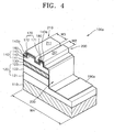
- FIG. 4 is a perspective view of a semiconductor laser diode according to an embodiment of the present invention.
- the illustration of the semiconductor laser diode of FIG. 4 has been exaggerated to show characteristics of the semiconductor laser diode according to the present invention more clearly.
- the semiconductor laser diode according to this embodiment of the present invention is a GaN-based, group III-V nitride semiconductor laser diode.
- the semiconductor laser diode 100a comprises a substrate 110, a first material layer 120, an active layer 130, and a second material layer 140 that are sequentially mounted on the substrate 110.
- the substrate 110 may be a GaN or SiC-based, group III-V semiconductor layer substrate or a high resistance substrate such as a sapphire substrate.
- the active layer 130 is a material layer of emitting light by carrier recombination of an electron and a hole.
- the active layer 130 is a GaN-based, group III-V nitride semiconductor layer having a multi quantum well (MQW) and more preferably, an In x Al y Ga 1-x-y layer where 0 ⁇ x ⁇ 1, 0 ⁇ y ⁇ 1, and x+y ⁇ 1.
- the active layer 130 may also be a GaN-based, group III-V nitride semiconductor layer containing a predetermined ratio of Indium (In), for example, an InGaN layer.
- the first material layer 120 comprises a buffer layer 121, a first cladding layer 122, and a first waveguide layer 123 that are sequentially mounted on the upper surface of the substrate 110.
- the second material layer 140 comprises a second waveguide layer 141, a second cladding layer 142, and a cap layer 143 that are sequentially mounted on the upper surface of the active layer 130.
- a bottom layer of the first material layer 120 is the buffer layer 121 and a top layer of the second material layer 140 is the cap layer 143.
- the buffer layer 121 is an n-type material layer made of a GaN-based, group III-V nitride semiconductor or an undoped material layer.
- the buffer layer 121 is an n-GaN layer.
- the cap layer 143 is a GaN-based, group III-V nitride semiconductor layer, preferably a p-type conductive impurity-doped direct transition layer, and more preferably a p-GaN layer.
- the cap layer 143 may be a GaN layer, an AIGaN layer or InGaN layer containing a predetermined ratio of AI or In, like the buffer layer 121.
- the first and second waveguide layers 123 and 141 are GaN-based, group III-V nitride semiconductor layers, and preferably, an n-GaN layer and a p-GaN layer, respectively.
- the first and second waveguide layers 123 and 141 have a reflective index lower than the active layer 130 and higher than the first cladding layer 122 and the second cladding layer 142 as will be described later.
- the first cladding layer 122 is an n-AIGaN/GaN layer and the second cladding layer 142 is the same material layer as the first cladding layer 122 except that a p-type material is doped.
- the semiconductor laser diode 100a comprises an n-type electrode layer 190a and a p-type electrode layer 170 as first and second electrode layers, which are electrically connected to the buffer layer 121 and the cap layer 143, respectively.
- a reference numeral 160 indicates a current restricting layer, which defines a channel 180 as a passage for limited contact between the p-type electrode layer 170 and the cap layer 143.
- the cap layer 143 is divided into first and second regions 143a and 143b.
- the cap layer 143 and the partially exposed second cladding layer 142 are covered with the current restricting layer 160.
- the current restricting layer 160 covering the first region 143a of the cap layer 143 is removed to expose the cap layer 143.
- the channel 180 is formed and the p-type electrode layer 170 and the cap layer 143 are limitedly in contact with each other through the channel 180.
- the channel 180 is filled with a contact layer 171 and a bonding metal layer 172 is formed on the upper surfaces of the contact layer 171 and the current restricting layer 160.
- the p-type electrode layer 170 is designated a layer containing the contact layer 171 and the bonding metal layer 172.
- a ridge waveguide 200 is formed at the first region 143a of the cap layer 143 and a first protrusion 210 is formed at the second region 143b of the cap layer 143.
- the first protrusion 210 is formed with a width wider than the width W 2 of the ridge waveguide 200.
- the ridge waveguide 200 has a width W2 of no more than several micrometers.
- the width W4 of the semiconductor laser diode 100a is about 200 ⁇ m.
- the first protrusion 210 may be separated from one side of the ride waveguide 200 by about 10 ⁇ m and be formed with a width W3 of about 50 to 100 ⁇ m.
- the width W3 of the first protrusion 210 is formed to be wider than that W2 of the ridge waveguide 200, but is not limited to the aforementioned range.
- the upper surface 211 of the first protrusion 210 is formed to be at the same height as the upper surface 201 of the ridge waveguide 200 and more preferably, to be at a slightly higher height than the upper surface 201 of the ridge waveguide 200.
- the upper surface of the contact layer 171 is formed to be at a height equal to or slightly lower than the upper surface of the current restricting layer 160 on the second region 143b of the cap layer 143 and then the bonding metal layer 172 is formed to the same thickness.
- various approaches such as formation of the bonding metal layer 172 at the second region 143b of the cap layer 143 thicker than that at the first region 143a of the cap layer 143 may be considered.
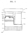
- FIG. 5 is a sectional view of a flip-chip bonded structure of a submount and the semiconductor laser diode shown in FIG. 4 in a semiconductor laser diode assembly according to an embodiment of the present invention.
- the submount 410 is a heat discharge structure for preventing overheating of the semiconductor laser diode 100a by heat generated in an active layer during laser emission.
- a reference numeral 411 indicates a substrate
- reference numerals 412a and 412b indicate first and second metal layers, respectively
- reference numerals 413a and 413b indicate first and second solder layers, respectively.
- the substrate 411 is made of one of AIN, SiC, GaN, and an insulating material having a heat transfer coefficient corresponding to that of one of AIN, SiC, and GaN.
- the first and second metal layers 412a and 412b are made of an Au/Cr alloy or a metal material corresponding to the Au/Cr alloy.
- the first and second solder layers 413a and 413b are made of an Au/Sn alloy or a metal material corresponding to the Au/Sn alloy.
- the first solder layer 413a is fused to the n-type electrode layer 190a and the second solder layer 413b is fused to the p-type electrode layer 170.
- the ridge waveguide 200 and the first protrusion 210 are positioned in the region of the p-type electrode layer 170, and thus, the second solder layer 413b is fused to the ridge waveguide 200 and the first protrusion 210.
- the first protrusion 210 with not less height than the ridge waveguide 200 is formed at one side of the ridge waveguide 200. Therefore, when the semiconductor laser diode 100a is bonded to the submount 410, the second solder layer 413b comes in contact with the first protrusion 210 and the ridge waveguide 200 at the same time or with first protrusion 210 first. Then, the second solder layer 413b is molten and spontaneously bonded to the ridge waveguide 200 and the first protrusion 210.
- a thermal stress generated during flip-chip bonding is dispersed to the first protrusion 210 adjacent to the ridge waveguide 200. Therefore, uneven light emission due to concentration of a thermal stress on the ridge waveguide can be prevented.
- the first and second solder layers 413a and 413b are not concurrently molten due to their thickness differences, a mechanical stress is dispersed to the first protrusion 210 with a width wider than the width of the ridge waveguide 200, and thus, the concentration of a mechanical stress on the ridge waveguide 200 can be prevented.
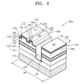
- FIG. 6 is a perspective view of a semiconductor laser diode according to another embodiment of the present invention.
- the same reference numerals as used in FIG. 4 indicate the same constitutional elements.
- the semiconductor laser diode 100b further comprises a second protrusion 220 at the other side of the ridge waveguide 200, that is, at the opposite side of the first protrusion 210.
- the second protrusion 220 is separated from the ridge waveguide 200 by a valley portion 230, which is etched to expose the buffer layer 121.
- the second protrusion 200 has a structure comprising the first material layer 120, the active layer 130, the second material layer 140, and the current restricting layer 160 that are sequentially mounted on the substrate 110, and an n-type electrode layer 190b mounted on the current restricting layer 160 to be electrically connected to the buffer layer 121.
- the n-type electrode layer 190b is a top layer of the second protrusion 220 and extends to the bottom surface 231 of the valley portion 230, to thereby be in contact with the buffer layer 121.
- the upper surface 221 of the second protrusion 220 is formed to be at the same height as the upper surface 201 of the ridge waveguide 200 and more preferably, at a slightly higher height than the upper surface 201 of the ridge waveguide 200.
- the top layer of the second protrusion 220 is the n-type electrode layer 190b electrically connected to the buffer layer 121.
- the second protrusion 220 may has the same height as the first protrusion 210. If the first and second protrusions 210 and 220 differ in height, it is preferable to limit the height difference to 0.5 ⁇ m or less.
- FIG. 7 is a sectional view of a flip-chip bonded structure of a submount and the semiconductor laser diode shown in FIG. 6 in a semiconductor laser diode assembly according to another embodiment of the present invention.
- the submount 420 comprises a substrate 421, first and second metal layers 422a and 422b, and first and second solder layers 423a and 423b.
- the submount 420 differs from the submount 410 shown in FIG. 5 in that the n-type electrode 190b is the top layer of the second protrusion 220 and the first and second solder layers 423a and 423b have the same thickness due to the same height of the first and second protrusions 210 and 220.
- the first and second solder layers 423a and 423b can be formed in a single process, and thus, can have almost the same chemical composition ratios.
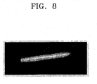
- FIG. 8 is an image plane photograph of laser light emission in the semiconductor laser diode assembly shown in FIG. 7. It can be seen from FIG. 8 that uniform and continuous light emission occurs along the ridge waveguide, unlike in FIG. 3.
- FIG. 9 is a perspective view of a semiconductor laser diode according to another embodiment of the present invention.
- the same reference numerals as used in FIGS. 4 through 7 indicate the same constitutional elements.
- the semiconductor laser diode 100c differs from the semiconductor laser diode 100b shown in FIG. 6 in that an n-type electrode layer 190c serves as the second protrusion 220.
- an exposed surface 240 of the buffer layer 121 is formed at the other side of the ridge waveguide 200, that is, at the opposite side of the first protrusion 210 and the n-type electrode layer 190c is mounted on the exposed surface 240.
- the n-type electrode layer 190c has not less height than the ridge waveguide 200.
- the width W6 of the n-type electrode layer 190c is wider than that W2 of the ridge waveguide 200.
- the n-type electrode layer 190c has the same height as the first protrusion 210.
- the n-type electrode layer 190c serves as the second protrusion 220 of FIG. 6. Therefore, the structural advantages obtained by using the n-type electrode layer 190c are as described with reference to FIGS. 6 and 7.
- a semiconductor laser diode and a semiconductor laser diode assembly of the present invention provide the following advantages.
- a thermal stress generated upon flip-chip bonding can be dispersed to the first protrusion adjacent to the ridge waveguide.
- the semiconductor laser diode further comprises the second protrusion, and thus, a mechanical stress generated by time difference melting of the solder layers of the submount can be effectively dispersed. Therefore, a laser diode and its assembly with uniform light emission throughout the ridge waveguide can be provided.
Landscapes
- Physics & Mathematics (AREA)
- Electromagnetism (AREA)
- Optics & Photonics (AREA)
- Condensed Matter Physics & Semiconductors (AREA)
- General Physics & Mathematics (AREA)
- Engineering & Computer Science (AREA)
- Plasma & Fusion (AREA)
- Semiconductor Lasers (AREA)
Applications Claiming Priority (2)
| Application Number | Priority Date | Filing Date | Title |
|---|---|---|---|
| KR1020030014614A KR100964399B1 (ko) | 2003-03-08 | 2003-03-08 | 반도체 레이저 다이오드 및 이를 채용한 반도체 레이저다이오드 조립체 |
| KR2003014614 | 2003-03-08 |
Publications (3)
| Publication Number | Publication Date |
|---|---|
| EP1469569A2 true EP1469569A2 (fr) | 2004-10-20 |
| EP1469569A3 EP1469569A3 (fr) | 2005-07-27 |
| EP1469569B1 EP1469569B1 (fr) | 2007-01-24 |
Family
ID=32906595
Family Applications (1)
| Application Number | Title | Priority Date | Filing Date |
|---|---|---|---|
| EP03258213A Expired - Lifetime EP1469569B1 (fr) | 2003-03-08 | 2003-12-23 | Système de diode laser à semi-conducteur |
Country Status (6)
| Country | Link |
|---|---|
| US (2) | US7180927B2 (fr) |
| EP (1) | EP1469569B1 (fr) |
| JP (1) | JP2004274058A (fr) |
| KR (1) | KR100964399B1 (fr) |
| CN (1) | CN100421320C (fr) |
| DE (1) | DE60311422T2 (fr) |
Families Citing this family (18)
| Publication number | Priority date | Publication date | Assignee | Title |
|---|---|---|---|---|
| KR100964399B1 (ko) * | 2003-03-08 | 2010-06-17 | 삼성전자주식회사 | 반도체 레이저 다이오드 및 이를 채용한 반도체 레이저다이오드 조립체 |
| US7773330B2 (en) * | 2005-04-15 | 2010-08-10 | Seagate Technology Llc | Apparatus for excitation, enhancement, and confinement of surface electromagnetic waves for confined optical power delivery |
| KR101100425B1 (ko) * | 2005-05-07 | 2011-12-30 | 삼성전자주식회사 | 반도체 레이저 다이오드 및 그 제조방법 |
| JP2007103460A (ja) * | 2005-09-30 | 2007-04-19 | Sanyo Electric Co Ltd | 半導体レーザ素子およびその製造方法 |
| US7643248B2 (en) * | 2006-06-30 | 2010-01-05 | Seagate Technology Llc | Optoelectronic emitter mounted on a slider |
| EP1906496B1 (fr) * | 2006-09-29 | 2010-01-06 | OSRAM Opto Semiconductors GmbH | Laser semi-conducteur et son procédé de fabrication |
| TWI502768B (zh) * | 2009-12-31 | 2015-10-01 | Epistar Corp | 光電半導體裝置及其製造方法 |
| JP2012248812A (ja) * | 2011-05-31 | 2012-12-13 | Sumitomo Electric Ind Ltd | 半導体光集積素子の製造方法 |
| US8451695B2 (en) | 2011-06-23 | 2013-05-28 | Seagate Technology Llc | Vertical cavity surface emitting laser with integrated mirror and waveguide |
| US20130322481A1 (en) * | 2012-05-31 | 2013-12-05 | Rajaram Bhat | Laser diodes including substrates having semipolar surface plane orientations and nonpolar cleaved facets |
| US9107316B2 (en) * | 2013-09-11 | 2015-08-11 | Eastman Kodak Company | Multi-layer micro-wire substrate structure |
| CN104538844B (zh) * | 2015-01-27 | 2018-10-26 | 中国科学院上海微系统与信息技术研究所 | 太赫兹量子级联激光器器件结构及其制作方法 |
| JP6654503B2 (ja) * | 2016-05-02 | 2020-02-26 | 日本電信電話株式会社 | 光半導体素子および半導体モノリシック型光回路 |
| CN115548878B (zh) * | 2021-06-29 | 2025-10-17 | 青岛联智光通信技术有限公司 | 一种具有调制器的激光芯片、准备方法及光模块 |
| JP7648763B2 (ja) * | 2021-06-30 | 2025-03-18 | 京セラ株式会社 | 発光体、発光体の製造方法および製造装置、発光素子およびその製造方法、並びに電子機器 |
| CN117096725A (zh) * | 2022-05-12 | 2023-11-21 | 常州承芯半导体有限公司 | 垂直腔面发射激光器及其形成方法 |
| CN116014560A (zh) * | 2022-12-07 | 2023-04-25 | 平湖科谱激光科技有限公司 | Dfb激光器及其制备方法 |
| FR3150343A1 (fr) * | 2023-06-22 | 2024-12-27 | Thales | Composant optoélectronique à crête enterré à haute puissande |
Family Cites Families (46)
| Publication number | Priority date | Publication date | Assignee | Title |
|---|---|---|---|---|
| JPS52116185A (en) * | 1976-03-26 | 1977-09-29 | Hitachi Ltd | Mesa-type semiconductor laser |
| US5022036A (en) * | 1988-12-29 | 1991-06-04 | Sharp Kabushiki Kaisha | Semiconductor laser device |
| JP2892053B2 (ja) * | 1989-10-30 | 1999-05-17 | 株式会社リコー | 半導体発光素子アレイ |
| ES2109231T3 (es) * | 1989-10-31 | 1998-01-16 | Furukawa Electric Co Ltd | Elementos laser de semi-conductores y metodo de fabricacion. |
| US5536085A (en) * | 1995-03-30 | 1996-07-16 | Northern Telecom Limited | Multi-wavelength gain-coupled distributed feedback laser array with fine tunability |
| JP3342322B2 (ja) * | 1996-11-27 | 2002-11-05 | シャープ株式会社 | Led素子表示装置の製造方法 |
| US6185238B1 (en) * | 1997-02-21 | 2001-02-06 | Kabushiki Kaisha Toshiba | Nitride compound semiconductor laser and its manufacturing method |
| US5936994A (en) * | 1997-09-18 | 1999-08-10 | Northern Telecom Limited | Two-section complex coupled distributed feedback semiconductor laser with enhanced wavelength tuning range |
| US20020028390A1 (en) * | 1997-09-22 | 2002-03-07 | Mohammad A. Mazed | Techniques for fabricating and packaging multi-wavelength semiconductor laser array devices (chips) and their applications in system architectures |
| US5917847A (en) * | 1997-09-26 | 1999-06-29 | Xerox Corporation | Independently addressable semiconductor laser arrays with buried selectively oxidized native oxide apertures |
| TW417320B (en) * | 1998-06-18 | 2001-01-01 | Ind Tech Res Inst | Self-aligned method for fabricating a ridge-waveguide semiconductor laser diode |
| JP3348024B2 (ja) * | 1998-08-17 | 2002-11-20 | 松下電器産業株式会社 | 半導体レーザ装置 |
| JP2000208871A (ja) * | 1999-01-19 | 2000-07-28 | Oki Electric Ind Co Ltd | 導波路型光素子,導波路型光素子の製造方法,光モジュ―ル,及び光モジュ―ルの製造方法 |
| US7212556B1 (en) * | 1999-02-17 | 2007-05-01 | Matsushita Electric Industrial Co., Ltd. | Semiconductor laser device optical disk apparatus and optical integrated unit |
| US6757313B1 (en) * | 1999-11-12 | 2004-06-29 | Trumpf Photonics Inc. | Control of current spreading in semiconductor laser diodes |
| WO2001035506A1 (fr) * | 1999-11-12 | 2001-05-17 | Princeton Lightwave, Inc. | Commande de la repartition du courant dans des diodes lasers a semi-conducteurs |
| US6410942B1 (en) * | 1999-12-03 | 2002-06-25 | Cree Lighting Company | Enhanced light extraction through the use of micro-LED arrays |
| JP2001168442A (ja) * | 1999-12-07 | 2001-06-22 | Sony Corp | 半導体レーザ素子の製造方法、配設基板および支持基板 |
| JP2001251018A (ja) * | 2000-03-03 | 2001-09-14 | Toyoda Gosei Co Ltd | Iii族窒化物系化合物半導体レーザ |
| KR100763829B1 (ko) * | 2000-06-08 | 2007-10-05 | 니치아 카가쿠 고교 가부시키가이샤 | 반도체 레이저 소자 및 그 제조방법 |
| JP2002171021A (ja) * | 2000-11-30 | 2002-06-14 | Toshiba Corp | 半導体レーザ、半導体レーザの製造方法および半導体レーザの実装方法 |
| US6791119B2 (en) * | 2001-02-01 | 2004-09-14 | Cree, Inc. | Light emitting diodes including modifications for light extraction |
| JP3889933B2 (ja) * | 2001-03-02 | 2007-03-07 | シャープ株式会社 | 半導体発光装置 |
| JP2003008143A (ja) | 2001-06-18 | 2003-01-10 | Sony Corp | マルチビーム半導体レーザ素子 |
| JP2002111137A (ja) | 2001-07-13 | 2002-04-12 | Matsushita Electric Ind Co Ltd | 半導体レーザ素子 |
| JP2003069153A (ja) * | 2001-08-29 | 2003-03-07 | Hitachi Ltd | 半導体光デバイス及び集積型光半導体装置 |
| JP4131623B2 (ja) * | 2001-09-12 | 2008-08-13 | 三洋電機株式会社 | 電極構造およびその製造方法 |
| JP3786000B2 (ja) * | 2001-12-14 | 2006-06-14 | 日亜化学工業株式会社 | 窒化物半導体レーザダイオードとその製造方法 |
| WO2003063312A1 (fr) * | 2002-01-21 | 2003-07-31 | Matsushita Electric Industrial Co., Ltd. | Dispositif laser a semi-conducteurs a base de nitrures et son procede de fabrication |
| JP2003264334A (ja) * | 2002-03-08 | 2003-09-19 | Hitachi Ltd | 半導体レーザ素子及び半導体レーザモジュール |
| DE10219886B4 (de) * | 2002-05-03 | 2007-10-04 | Chunghwa Telecom Co.Ltd. | Selbstjustierendes Verfahren zur Herstellung eines Stegwellenleiter-Halbleiterlasers |
| JP2003332676A (ja) * | 2002-05-08 | 2003-11-21 | Mitsubishi Electric Corp | 半導体光装置 |
| JP2004014938A (ja) * | 2002-06-10 | 2004-01-15 | Matsushita Electric Ind Co Ltd | 半導体装置及びその製造方法 |
| JP4480948B2 (ja) * | 2002-07-15 | 2010-06-16 | 日本オプネクスト株式会社 | 半導体レーザ素子及びその製造方法 |
| TWI303909B (en) * | 2002-11-25 | 2008-12-01 | Nichia Corp | Ridge waveguide semiconductor laser diode |
| KR100958054B1 (ko) * | 2003-03-08 | 2010-05-13 | 삼성전자주식회사 | 반도체 레이저 다이오드의 서브 마운트, 그 제조방법 및이를 채용한 반도체 레이저 다이오드 조립체 |
| KR100964399B1 (ko) * | 2003-03-08 | 2010-06-17 | 삼성전자주식회사 | 반도체 레이저 다이오드 및 이를 채용한 반도체 레이저다이오드 조립체 |
| KR20040092764A (ko) * | 2003-04-29 | 2004-11-04 | 삼성전자주식회사 | 자기정렬을 이용한 반도체 레이저 다이오드 및 그 제조방법 |
| TWI347054B (en) * | 2003-07-11 | 2011-08-11 | Nichia Corp | Nitride semiconductor laser device and method of manufacturing the nitride semiconductor laser device |
| US7250631B2 (en) * | 2003-10-14 | 2007-07-31 | Nichia Corporation | Semiconductor laser having protruding portion |
| ATE418806T1 (de) * | 2004-04-02 | 2009-01-15 | Nichia Corp | Nitrid-halbleiterlaservorrichtung |
| JP4956928B2 (ja) * | 2004-09-28 | 2012-06-20 | 日亜化学工業株式会社 | 半導体装置 |
| KR20060115453A (ko) * | 2005-05-06 | 2006-11-09 | 삼성전자주식회사 | 방열 구조체 및 이를 구비한 발광소자 조립체 |
| KR101100425B1 (ko) * | 2005-05-07 | 2011-12-30 | 삼성전자주식회사 | 반도체 레이저 다이오드 및 그 제조방법 |
| US9153645B2 (en) * | 2005-05-17 | 2015-10-06 | Taiwan Semiconductor Manufacturing Company, Ltd. | Lattice-mismatched semiconductor structures with reduced dislocation defect densities and related methods for device fabrication |
| JPWO2007135772A1 (ja) * | 2006-05-19 | 2009-10-01 | 日本電気株式会社 | 発光素子 |
-
2003
- 2003-03-08 KR KR1020030014614A patent/KR100964399B1/ko not_active Expired - Fee Related
- 2003-12-11 US US10/732,240 patent/US7180927B2/en not_active Expired - Lifetime
- 2003-12-23 EP EP03258213A patent/EP1469569B1/fr not_active Expired - Lifetime
- 2003-12-23 DE DE60311422T patent/DE60311422T2/de not_active Expired - Lifetime
- 2003-12-30 CN CNB2003101243426A patent/CN100421320C/zh not_active Expired - Lifetime
-
2004
- 2004-03-05 JP JP2004062196A patent/JP2004274058A/ja active Pending
-
2007
- 2007-01-09 US US11/650,991 patent/US20070110113A1/en not_active Abandoned
Also Published As
| Publication number | Publication date |
|---|---|
| CN100421320C (zh) | 2008-09-24 |
| US20070110113A1 (en) | 2007-05-17 |
| CN1527451A (zh) | 2004-09-08 |
| KR100964399B1 (ko) | 2010-06-17 |
| US20040174918A1 (en) | 2004-09-09 |
| EP1469569A3 (fr) | 2005-07-27 |
| US7180927B2 (en) | 2007-02-20 |
| EP1469569B1 (fr) | 2007-01-24 |
| KR20040079636A (ko) | 2004-09-16 |
| JP2004274058A (ja) | 2004-09-30 |
| DE60311422D1 (de) | 2007-03-15 |
| DE60311422T2 (de) | 2007-10-18 |
Similar Documents
| Publication | Publication Date | Title |
|---|---|---|
| US20070110113A1 (en) | Semiconductor laser diode and semiconductor laser diode assembly containing the same | |
| US7092420B2 (en) | Submount of semiconductor laser diode, method of manufacturing the same, and semiconductor laser diode assembly using the submount | |
| US11626707B2 (en) | Semiconductor laser diode | |
| CN114243448B (zh) | 半导体激光二极管 | |
| US7566578B2 (en) | GaN based group III-V nitride semiconductor light-emitting diode and method for fabricating the same | |
| US6185238B1 (en) | Nitride compound semiconductor laser and its manufacturing method | |
| US7745839B2 (en) | Double wavelength semiconductor light emitting device and method of manufacturing the same | |
| US20090039359A1 (en) | Light emitting diode with improved current spreading performance | |
| US12483006B2 (en) | Edge-emitting laser bar | |
| US7406111B2 (en) | Semiconductor laser diode and method for manufacturing the same | |
| JPH10223930A (ja) | 半導体発光素子 | |
| JPH10308560A (ja) | 半導体発光素子および発光装置 | |
| US7606275B2 (en) | Semiconductor laser device having incomplete bonding region and electronic equipment | |
| KR100397608B1 (ko) | GaN계열 Ⅲ-Ⅴ족 질화물 반도체 레이저 다이오드 | |
| KR100922847B1 (ko) | 레이저 다이오드 및 그 제조방법 | |
| JP2010098001A (ja) | 半導体レーザ装置およびその製造方法 |
Legal Events
| Date | Code | Title | Description |
|---|---|---|---|
| PUAI | Public reference made under article 153(3) epc to a published international application that has entered the european phase |
Free format text: ORIGINAL CODE: 0009012 |
|
| AK | Designated contracting states |
Kind code of ref document: A2 Designated state(s): AT BE BG CH CY CZ DE DK EE ES FI FR GB GR HU IE IT LI LU MC NL PT RO SE SI SK TR |
|
| AX | Request for extension of the european patent |
Extension state: AL LT LV MK |
|
| PUAL | Search report despatched |
Free format text: ORIGINAL CODE: 0009013 |
|
| AK | Designated contracting states |
Kind code of ref document: A3 Designated state(s): AT BE BG CH CY CZ DE DK EE ES FI FR GB GR HU IE IT LI LU MC NL PT RO SE SI SK TR |
|
| AX | Request for extension of the european patent |
Extension state: AL LT LV MK |
|
| 17P | Request for examination filed |
Effective date: 20051130 |
|
| AKX | Designation fees paid |
Designated state(s): DE FR GB |
|
| GRAP | Despatch of communication of intention to grant a patent |
Free format text: ORIGINAL CODE: EPIDOSNIGR1 |
|
| RTI1 | Title (correction) |
Free format text: SEMICONDUCTOR LASER DIODE ASSEMBLY |
|
| GRAS | Grant fee paid |
Free format text: ORIGINAL CODE: EPIDOSNIGR3 |
|
| GRAA | (expected) grant |
Free format text: ORIGINAL CODE: 0009210 |
|
| AK | Designated contracting states |
Kind code of ref document: B1 Designated state(s): DE FR GB |
|
| REG | Reference to a national code |
Ref country code: GB Ref legal event code: FG4D |
|
| REF | Corresponds to: |
Ref document number: 60311422 Country of ref document: DE Date of ref document: 20070315 Kind code of ref document: P |
|
| ET | Fr: translation filed | ||
| PLBE | No opposition filed within time limit |
Free format text: ORIGINAL CODE: 0009261 |
|
| STAA | Information on the status of an ep patent application or granted ep patent |
Free format text: STATUS: NO OPPOSITION FILED WITHIN TIME LIMIT |
|
| 26N | No opposition filed |
Effective date: 20071025 |
|
| REG | Reference to a national code |
Ref country code: FR Ref legal event code: PLFP Year of fee payment: 13 |
|
| REG | Reference to a national code |
Ref country code: FR Ref legal event code: PLFP Year of fee payment: 14 |
|
| REG | Reference to a national code |
Ref country code: FR Ref legal event code: PLFP Year of fee payment: 15 |
|
| PGFP | Annual fee paid to national office [announced via postgrant information from national office to epo] |
Ref country code: GB Payment date: 20221103 Year of fee payment: 20 Ref country code: FR Payment date: 20221110 Year of fee payment: 20 Ref country code: DE Payment date: 20220622 Year of fee payment: 20 |
|
| P01 | Opt-out of the competence of the unified patent court (upc) registered |
Effective date: 20230520 |
|
| REG | Reference to a national code |
Ref country code: DE Ref legal event code: R071 Ref document number: 60311422 Country of ref document: DE |
|
| REG | Reference to a national code |
Ref country code: GB Ref legal event code: PE20 Expiry date: 20231222 |
|
| PG25 | Lapsed in a contracting state [announced via postgrant information from national office to epo] |
Ref country code: GB Free format text: LAPSE BECAUSE OF EXPIRATION OF PROTECTION Effective date: 20231222 |
|
| PG25 | Lapsed in a contracting state [announced via postgrant information from national office to epo] |
Ref country code: GB Free format text: LAPSE BECAUSE OF EXPIRATION OF PROTECTION Effective date: 20231222 |