EP1472604B1 - Umkonfigurierbares parallelnachschlagetabellensystem - Google Patents
Umkonfigurierbares parallelnachschlagetabellensystem Download PDFInfo
- Publication number
- EP1472604B1 EP1472604B1 EP02784666A EP02784666A EP1472604B1 EP 1472604 B1 EP1472604 B1 EP 1472604B1 EP 02784666 A EP02784666 A EP 02784666A EP 02784666 A EP02784666 A EP 02784666A EP 1472604 B1 EP1472604 B1 EP 1472604B1
- Authority
- EP
- European Patent Office
- Prior art keywords
- look
- index register
- tables
- values
- memory
- Prior art date
- Legal status (The legal status is an assumption and is not a legal conclusion. Google has not performed a legal analysis and makes no representation as to the accuracy of the status listed.)
- Expired - Lifetime
Links
Images




Classifications
-
- G—PHYSICS
- G06—COMPUTING OR CALCULATING; COUNTING
- G06F—ELECTRIC DIGITAL DATA PROCESSING
- G06F9/00—Arrangements for program control, e.g. control units
- G06F9/06—Arrangements for program control, e.g. control units using stored programs, i.e. using an internal store of processing equipment to receive or retain programs
- G06F9/30—Arrangements for executing machine instructions, e.g. instruction decode
- G06F9/34—Addressing or accessing the instruction operand or the result ; Formation of operand address; Addressing modes
- G06F9/345—Addressing or accessing the instruction operand or the result ; Formation of operand address; Addressing modes of multiple operands or results
-
- G—PHYSICS
- G06—COMPUTING OR CALCULATING; COUNTING
- G06F—ELECTRIC DIGITAL DATA PROCESSING
- G06F12/00—Accessing, addressing or allocating within memory systems or architectures
- G06F12/02—Addressing or allocation; Relocation
- G06F12/0207—Addressing or allocation; Relocation with multidimensional access, e.g. row/column, matrix
Definitions
- This invention relates to a reconfigurable parallel look-up table system
- Prior art patent US6,223,320 discloses an improved CRC generation mechanism comprising a parallel table lookup operation preferably performed using a vector permute instruction that performs the following operations in parallel: selects data elements from a source vector register VA based upon indices stored as data elements in a source vector register VB, and writes the selected data elements into a target vector register VT.
- the invention results from the realization that a truly faster and more flexible look-up table system can be achieved by enabling a number of look-up tables in a memory to be accessed simultaneously by combining the values to be looked up with the values representing the starting addresses of the look-up tables to simultaneously translate each value into an address to locate in parallel the function of those values in each look-up table.
- This invention features a reconfigurable parallel look-up table system including a memory and a plurality of look-up tables stored on the memory.
- a row index register holds the values to be looked up in the look-up tables, and the column index register stores the value representing the starting address of each of the look-up tables stored in the memory.
- An address translation circuit is responsive to the column index register and the row index register to simultaneously generate an address for each value in the row index register to locate in parallel the functions of those values in each look-up table.
- the address translation circuit may include a multiplier circuit for multiplying the value representing the starting address by the length of each column and an adder circuit for combining the value in the row index register with the output of the multiplier circuit.
- the address translation circuit may include an OR circuit for combining the values from the row index register with the values in the column index register shifted toward the MSB by N bits in respect to the values in the row index register.
- the look-up tables may be all the same size.
- FIG. 1 a reconfigurable parallel look-up table system 10 according to this invention which includes a row index register R 2 ,12 and a column index register R 1 , 14, an address translation circuit 16 and a memory 18 which contains a number of look-up tables.
- the output from memory 18 is delivered to output register 20.
- Memory 18 includes a number of look-up tables and row index register 12 holds the values to be looked up in those look-up tables.
- row index register 12 may hold the angles that are to be looked up in the look-up tables at memory 18 where each of the look-up tables has a different function, one of the sine value, cosine value, tangent value, and so on for those angles.
- Column index register 14 stores a value representing the starting address of each look-up table stored in the memory. For example, if memory 18 holds eight look-up tables of 64 bytes each, the starting points for those look-up tables which coincide with the columns 30, 32, 34, 36, 38, 40, 42, 44 will be 0, 64, 128, 192, 256, 320, 384, and 448.
- Address translation circuit 16 combines the value in the row index register 12 with a representation of the starting address of each of the look-up tables to simultaneously generate an address for each value in the index register to locate in parallel the function of those values in each look-up table.
- Memories are typically made in a linear fashion as shown in Fig. 3 for manufacturing convenience.
- a memory that has a storage capacity of 512 bytes each byte comprising eight bits will be constructed as indicated by memory 18a, Fig. 2 , where there are eight columns 30-44 running one after another and containing rows of bytes 0-63, 64-127,128-191,192-255, 256-319, 320-383, 384-447, 448-511.
- memory 18a will more likely be envisioned as memory 18b, Fig. 3 where each of the columns 30-44 are envisioned in side by side position each extending for sixty-four rows 46, numbered 0-63.
- Fig. 5 where the row index register 12b and the column index register 14b are shown as eight stage registers, each stage representing a byte, each byte of 8 bits.
- the first stage 60 resides the number four as previously, but in the first stage 62 of register 14b resides the number forty, because this number will be multiplied by eight due to a hardwired shift of three bits to provide the number 320 as previously explained.
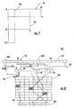
- the expanded view of stage 60, Fig. 6 shows the eight bit structure with a "1" in the third bit position, 64, representing binary four.
- Stage 62 of register 14b is shown with its eight bits having a "1" in the fourth and sixth bit position where the "1" bit at 66 represents an eight and the "1" bit at 68 represents thirty-two for a total of forty.
- the eight bits from stage 62 of register 14b have been shifted three bits to the left relative to the eight bits of stage 60 from register 12b. This effectively multiplies by eight the value in stage 62.
- reconfigurable parallel look-up system 10f includes row index register 12f and column index register 14f, each of which have eight stages as explained previously with respect to Fig. 6 and a memory 18f which includes eight columns of sixty-four bytes each as illustrated in Fig. 3 .
- the address translation circuit 16f includes a number of OR circuits.
- One OR circuit is associated with each pair of stages from each of registers 12f and 14f. There are thus eight OR circuits, only three of which are shown for clarity, 90, 92 and 94. In operation, OR circuit 90 receives five of the eight inputs from eight bit stage 60f, while the three remaining least significant bits from stage 60 are delivered directly to the memory address bus 96.
- OR gate 90 The other inputs to OR gate 90 are six bits from the first stage 62f of register 14f. These are combined as explained with respect to Fig. 6 so that the five bits from stage 60f and the six bits from the shifted stage 62f are OR-ed to produce a six bit output which is then combined with the three least significant bits from stage 60f to provide the nine bit address on address bus 96.
- OR circuits 92 and 94 and the other OR circuits omitted for clarity operate in the same way to address locations in memory 18f.
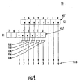
- Each OR circuit as exemplified by OR circuit 90, Fig. 9 includes five OR gates, 100, 102, 104, 106 and 108 which combine the bits from the third, fourth, fifth, sixth and seventh positions of stage 60f with those from positions zero, one, two, three, and four of stage 62f, respectively, with the bits in stage 62 having been shifted by three places with respect to those in stage 60f.
- the first three bits zero, one, two of stage 60 f are delivered directly, not through OR gates, to provide the nine bit address zero-eight at the output 110.
- the most significant bit from position five in stage 62f is also fed directly and not through any OR gate.
- register 14g has stored in its stages 62g1 through 62g8 the values to be looked up, 0, 8, 16, 24, 32, 40, 48, and 56, respectively.
- the starting points of each look-up table will be respectively 0, 64, 128, 192, 256, 320, 384, and 448 as previously explained.
- the values to be looked up in the look-up tables are stored in each of the stages 60gl-60g8, these values can be stored in merely six bits since there are only sixty-four row addresses in each column or look-up table.
- the combination of the two values in the stages of registers 14g and 12g are accomplished as previously explained by the shifting and adding accomplished in the OR circuits 150,152, 154, 156, 158, 160, 162, and 164.
- the reconfigurable parallel look-up table system 10h can be configured to serve two look-up tables, each of 256 bytes by placing the values 32 in each of stages 62h1-62h4 and zeros in the remaining stages 62h5-52h8. By placing the 32's in the first four stages the first four values are going to use the look-up table starting at 256 and going to 511 and the other four values are going to use the look up table starting at zero and going to 255.
- the values in the stages of the row index register 12h will be expressed now in eight bit form since the number of rows is 256.
- stages 62h1-62h8 can be loaded alternately with the values 0 and 32, while the stages 60h1-60h8 can be loaded in like pairs so that 60h1 and 60h2 have the same value, 60h3 and 60h4 have the same value, and so on, so that sixteen bit words can be addressed and looked up with the least significant byte (LSB) using the table starting from 0 and going to 255 and the most significant byte (MSB) using the table starting from 256 and going to 511.
- LSB least significant byte
- MSB most significant byte
Landscapes
- Engineering & Computer Science (AREA)
- Theoretical Computer Science (AREA)
- Physics & Mathematics (AREA)
- Software Systems (AREA)
- General Engineering & Computer Science (AREA)
- General Physics & Mathematics (AREA)
- Mathematical Physics (AREA)
- Logic Circuits (AREA)
- Communication Control (AREA)
- Devices For Executing Special Programs (AREA)
- Small-Scale Networks (AREA)
- Exchange Systems With Centralized Control (AREA)
- Magnetic Ceramics (AREA)
Claims (4)
- Ein umkonfigurierbares Paralleinachschlagetabellensystem, aufweisend:Einen Speicher (18);eine Mehrzahl von Nachschlagetabellen, die in besagtem Speicher gespeichert sind;ein Zeilenindexregister (12) zum Halten der Werte, die in besagten Nachschlagetabellen nachgeschlagen werden sollten, gekennzeichnet durch:ein Spaltenindexregister (14) zum Speichern eines Wertes, der die Anfangsadresse jeder besagter Nachschlagetabelle, die in besagtem Speicher gespeichert ist, darstellt; undeine Adressenübersetzungsschaltung (16), die auf besagtes Spaltenindexregister und besagtes Zeilenindexregister anspricht, um gleichzeitig eine Adresse für jeden Wert in besagtem Zeilenindexregister zu erzeugen um parallel die Funktionen jener Werte in jeder Nachschlagetabelle zu finden.
- Das umkonfigurierbare Parallelnachschlagetabellensystem des Anspruchs 1,
in dem besagte Adressenübersetzungsschaltung eine Multiplizierschaltung (50) zum Multiplizieren des Wertes, der die Anfangsadresse darstellt, mit der Länge jeder Spalte, und eine Addierschaltung (52) zum Kombinieren des Wertes in besagtem Zeilenindexregister mit dem Ausgang besagter Multiplizierschaltung aufweist. - Das umkonfigurierbare Parallelnachschlagetabellensystem des Anspruchs 1,
in dem besagte Adressenübersetzungsschaltung eine ODER-Schaltung (90) zum Kombinieren besagter Werte in besagtem Zeilenindexregister und besagter Werte in besagtem Spaltenindexregister, zum höchstwertigen Bit um n Bit in Bezug auf die Werte in dem Zeilenindexregister verschoben, aufweist. - Das umkonfigurierbare Parallelnachschlagetabellensystem des Anspruchs 1,
in dem besagte Nachschlagetabellen alle die gleiche Größe haben.
Applications Claiming Priority (5)
| Application Number | Priority Date | Filing Date | Title |
|---|---|---|---|
| US35533702P | 2002-02-07 | 2002-02-07 | |
| US355337P | 2002-02-07 | ||
| US131007 | 2002-04-24 | ||
| US10/131,007 US6829694B2 (en) | 2002-02-07 | 2002-04-24 | Reconfigurable parallel look up table system |
| PCT/US2002/038261 WO2003067364A2 (en) | 2002-02-07 | 2002-11-27 | Reconfigurable parallel look up table system |
Publications (4)
| Publication Number | Publication Date |
|---|---|
| EP1472604A2 EP1472604A2 (de) | 2004-11-03 |
| EP1472604A4 EP1472604A4 (de) | 2008-03-26 |
| EP1472604B1 true EP1472604B1 (de) | 2009-03-18 |
| EP1472604B8 EP1472604B8 (de) | 2009-11-25 |
Family
ID=27668039
Family Applications (1)
| Application Number | Title | Priority Date | Filing Date |
|---|---|---|---|
| EP02784666A Expired - Lifetime EP1472604B8 (de) | 2002-02-07 | 2002-11-27 | Umkonfigurierbares parallelnachschlagetabellensystem |
Country Status (8)
| Country | Link |
|---|---|
| US (1) | US6829694B2 (de) |
| EP (1) | EP1472604B8 (de) |
| JP (1) | JP3947163B2 (de) |
| CN (1) | CN100545818C (de) |
| AT (1) | ATE426203T1 (de) |
| AU (1) | AU2002346595A1 (de) |
| DE (1) | DE60231658D1 (de) |
| WO (1) | WO2003067364A2 (de) |
Families Citing this family (24)
| Publication number | Priority date | Publication date | Assignee | Title |
|---|---|---|---|---|
| US7082452B2 (en) * | 2001-11-30 | 2006-07-25 | Analog Devices, Inc. | Galois field multiply/multiply-add/multiply accumulate |
| US7269615B2 (en) * | 2001-12-18 | 2007-09-11 | Analog Devices, Inc. | Reconfigurable input Galois field linear transformer system |
| US6766345B2 (en) | 2001-11-30 | 2004-07-20 | Analog Devices, Inc. | Galois field multiplier system |
| US7177891B2 (en) * | 2002-10-09 | 2007-02-13 | Analog Devices, Inc. | Compact Galois field multiplier engine |
| US7283628B2 (en) | 2001-11-30 | 2007-10-16 | Analog Devices, Inc. | Programmable data encryption engine |
| US7895253B2 (en) | 2001-11-30 | 2011-02-22 | Analog Devices, Inc. | Compound Galois field engine and Galois field divider and square root engine and method |
| US7508937B2 (en) * | 2001-12-18 | 2009-03-24 | Analog Devices, Inc. | Programmable data encryption engine for advanced encryption standard algorithm |
| US6865661B2 (en) * | 2002-01-21 | 2005-03-08 | Analog Devices, Inc. | Reconfigurable single instruction multiple data array |
| US7000090B2 (en) * | 2002-01-21 | 2006-02-14 | Analog Devices, Inc. | Center focused single instruction multiple data (SIMD) array system |
| US6941446B2 (en) * | 2002-01-21 | 2005-09-06 | Analog Devices, Inc. | Single instruction multiple data array cell |
| US7421076B2 (en) * | 2003-09-17 | 2008-09-02 | Analog Devices, Inc. | Advanced encryption standard (AES) engine with real time S-box generation |
| US7512647B2 (en) * | 2004-11-22 | 2009-03-31 | Analog Devices, Inc. | Condensed Galois field computing system |
| US8024551B2 (en) | 2005-10-26 | 2011-09-20 | Analog Devices, Inc. | Pipelined digital signal processor |
| US7728744B2 (en) * | 2005-10-26 | 2010-06-01 | Analog Devices, Inc. | Variable length decoder system and method |
| US8285972B2 (en) * | 2005-10-26 | 2012-10-09 | Analog Devices, Inc. | Lookup table addressing system and method |
| US7478119B2 (en) * | 2006-07-03 | 2009-01-13 | Sun Microsystems, Inc. | System and method for transposing memory patterns within the physical memory space |
| US8301990B2 (en) * | 2007-09-27 | 2012-10-30 | Analog Devices, Inc. | Programmable compute unit with internal register and bit FIFO for executing Viterbi code |
| DE102007051345A1 (de) * | 2007-10-26 | 2009-04-30 | Fraunhofer-Gesellschaft zur Förderung der angewandten Forschung e.V. | Explosivstoffladung |
| US8384722B1 (en) | 2008-12-17 | 2013-02-26 | Matrox Graphics, Inc. | Apparatus, system and method for processing image data using look up tables |
| US20110052059A1 (en) * | 2009-08-27 | 2011-03-03 | Canon Kabushiki Kaisha | Generating image histogram by parallel processing |
| US20120201373A1 (en) * | 2011-02-03 | 2012-08-09 | Futurewei Technologies, Inc. | Design of a Good General-Purpose Hash Function with Limited Resources |
| US9141131B2 (en) * | 2011-08-26 | 2015-09-22 | Cognitive Electronics, Inc. | Methods and systems for performing exponentiation in a parallel processing environment |
| US10936570B2 (en) | 2017-12-22 | 2021-03-02 | Teradata Us, Inc. | Online and dynamic table reconfiguration |
| JP2023077933A (ja) * | 2021-11-25 | 2023-06-06 | 日本無線株式会社 | 鋸波電圧生成器 |
Family Cites Families (18)
| Publication number | Priority date | Publication date | Assignee | Title |
|---|---|---|---|---|
| DE1181461B (de) | 1963-10-08 | 1964-11-12 | Telefunken Patent | Adressenaddierwerk einer programm-gesteuerten Rechenmaschine |
| US5101338A (en) | 1988-04-27 | 1992-03-31 | Nec Corporation | Memory access control device which can be formed by a reduced number of lsi's |
| US5062057A (en) * | 1988-12-09 | 1991-10-29 | E-Machines Incorporated | Computer display controller with reconfigurable frame buffer memory |
| US5386523A (en) | 1992-01-10 | 1995-01-31 | Digital Equipment Corporation | Addressing scheme for accessing a portion of a large memory space |
| KR0135846B1 (ko) | 1994-02-02 | 1998-06-15 | 김광호 | 룩-업-테이블장치 |
| US5832290A (en) | 1994-06-13 | 1998-11-03 | Hewlett-Packard Co. | Apparatus, systems and method for improving memory bandwidth utilization in vector processing systems |
| US5839072A (en) * | 1996-03-26 | 1998-11-17 | Ericsson Inc. | Routing an incoming call to a ported mobile station within a telecommunications network |
| US5996066A (en) | 1996-10-10 | 1999-11-30 | Sun Microsystems, Inc. | Partitioned multiply and add/subtract instruction for CPU with integrated graphics functions |
| US6223320B1 (en) | 1998-02-10 | 2001-04-24 | International Business Machines Corporation | Efficient CRC generation utilizing parallel table lookup operations |
| GB9806687D0 (en) * | 1998-03-27 | 1998-05-27 | Memory Corp Plc | Memory system |
| US6138208A (en) | 1998-04-13 | 2000-10-24 | International Business Machines Corporation | Multiple level cache memory with overlapped L1 and L2 memory access |
| US5996057A (en) | 1998-04-17 | 1999-11-30 | Apple | Data processing system and method of permutation with replication within a vector register file |
| US6446198B1 (en) * | 1999-09-30 | 2002-09-03 | Apple Computer, Inc. | Vectorized table lookup |
| US6539477B1 (en) * | 2000-03-03 | 2003-03-25 | Chameleon Systems, Inc. | System and method for control synthesis using a reachable states look-up table |
| US6480845B1 (en) * | 2000-06-14 | 2002-11-12 | Bull Hn Information Systems Inc. | Method and data processing system for emulating virtual memory working spaces |
| CN1232041C (zh) * | 2001-05-16 | 2005-12-14 | 皇家菲利浦电子有限公司 | 可重新配置的逻辑器件以及包括该器件的乘法阵列 |
| US7283628B2 (en) * | 2001-11-30 | 2007-10-16 | Analog Devices, Inc. | Programmable data encryption engine |
| US7508937B2 (en) * | 2001-12-18 | 2009-03-24 | Analog Devices, Inc. | Programmable data encryption engine for advanced encryption standard algorithm |
-
2002
- 2002-04-24 US US10/131,007 patent/US6829694B2/en not_active Expired - Lifetime
- 2002-11-27 EP EP02784666A patent/EP1472604B8/de not_active Expired - Lifetime
- 2002-11-27 AT AT02784666T patent/ATE426203T1/de not_active IP Right Cessation
- 2002-11-27 DE DE60231658T patent/DE60231658D1/de not_active Expired - Lifetime
- 2002-11-27 AU AU2002346595A patent/AU2002346595A1/en not_active Abandoned
- 2002-11-27 JP JP2003566649A patent/JP3947163B2/ja not_active Expired - Fee Related
- 2002-11-27 CN CNB028284852A patent/CN100545818C/zh not_active Expired - Fee Related
- 2002-11-27 WO PCT/US2002/038261 patent/WO2003067364A2/en not_active Ceased
Also Published As
| Publication number | Publication date |
|---|---|
| WO2003067364A3 (en) | 2003-10-02 |
| WO2003067364A2 (en) | 2003-08-14 |
| JP3947163B2 (ja) | 2007-07-18 |
| US6829694B2 (en) | 2004-12-07 |
| AU2002346595A8 (en) | 2003-09-02 |
| DE60231658D1 (de) | 2009-04-30 |
| US20030149857A1 (en) | 2003-08-07 |
| CN100545818C (zh) | 2009-09-30 |
| JP2005517233A (ja) | 2005-06-09 |
| EP1472604A2 (de) | 2004-11-03 |
| EP1472604B8 (de) | 2009-11-25 |
| ATE426203T1 (de) | 2009-04-15 |
| CN1623141A (zh) | 2005-06-01 |
| AU2002346595A1 (en) | 2003-09-02 |
| EP1472604A4 (de) | 2008-03-26 |
Similar Documents
| Publication | Publication Date | Title |
|---|---|---|
| EP1472604B1 (de) | Umkonfigurierbares parallelnachschlagetabellensystem | |
| USRE43552E1 (en) | Block programmable priority encoder in a cam | |
| US7577819B2 (en) | Vector indexed memory unit and method | |
| US20030103626A1 (en) | Programmable data encryption engine | |
| EP2130132B1 (de) | Dsp mit rechnereinheit mit interner bit-fifo-schaltung | |
| JP5112325B2 (ja) | 参照テーブルアドレス指定システム及び方法 | |
| JP2014038640A (ja) | 改善されたパイプライン化デジタル信号プロセッサ | |
| US9929744B2 (en) | Memory compression operable for non-contiguous write/read addresses | |
| JP2008542910A (ja) | バイトアドレシング可能メモリの抽出されたインデックスアドレシング | |
| US6640296B2 (en) | Data processing method and device for parallel stride access | |
| EP1649634B1 (de) | Verfahren und vorrichtung zur schnellen rc4-verschlüsselung | |
| US20120173598A1 (en) | Apparatus and method for division of a galois field binary polynomial | |
| JP3735105B2 (ja) | レジスタから並列テーブルルックアップを行う可変再配列(mux)命令 | |
| US7350019B2 (en) | Content addressable memory device capable of being used in cascaded fashion | |
| JP2003196156A (ja) | 情報処理装置および情報処理方法 | |
| KR100864363B1 (ko) | 부호화 회로 및 디지털 신호 처리 회로 | |
| CN102713875A (zh) | 包含组合的选择和数据对齐或数据复制的多级多路复用运算 | |
| US20160226878A1 (en) | Method and apparatus for use with different memory maps | |
| CN1608251A (zh) | 可重新配置输入的伽罗瓦域线性变换器系统 | |
| JPH04130549A (ja) | メモリ装置 | |
| JPH06250620A (ja) | プログラム式フォーマットビデオメモリ | |
| KR19980020083A (ko) | 데이터 보간방법 |
Legal Events
| Date | Code | Title | Description |
|---|---|---|---|
| PUAI | Public reference made under article 153(3) epc to a published international application that has entered the european phase |
Free format text: ORIGINAL CODE: 0009012 |
|
| 17P | Request for examination filed |
Effective date: 20040806 |
|
| AK | Designated contracting states |
Kind code of ref document: A2 Designated state(s): AT BE BG CH CY CZ DE DK EE ES FI FR GB GR IE IT LI LU MC NL PT SE SK TR |
|
| AX | Request for extension of the european patent |
Extension state: AL LT LV MK RO SI |
|
| A4 | Supplementary search report drawn up and despatched |
Effective date: 20080221 |
|
| RIC1 | Information provided on ipc code assigned before grant |
Ipc: G06F 9/345 20060101AFI20080215BHEP Ipc: G06F 12/02 20060101ALI20080215BHEP |
|
| GRAP | Despatch of communication of intention to grant a patent |
Free format text: ORIGINAL CODE: EPIDOSNIGR1 |
|
| GRAS | Grant fee paid |
Free format text: ORIGINAL CODE: EPIDOSNIGR3 |
|
| GRAA | (expected) grant |
Free format text: ORIGINAL CODE: 0009210 |
|
| AK | Designated contracting states |
Kind code of ref document: B1 Designated state(s): AT BE BG CH CY CZ DE DK EE ES FI FR GB GR IE IT LI LU MC NL PT SE SK TR |
|
| REG | Reference to a national code |
Ref country code: GB Ref legal event code: FG4D |
|
| REG | Reference to a national code |
Ref country code: CH Ref legal event code: EP |
|
| REG | Reference to a national code |
Ref country code: IE Ref legal event code: FG4D |
|
| REF | Corresponds to: |
Ref document number: 60231658 Country of ref document: DE Date of ref document: 20090430 Kind code of ref document: P |
|
| PG25 | Lapsed in a contracting state [announced via postgrant information from national office to epo] |
Ref country code: FI Free format text: LAPSE BECAUSE OF FAILURE TO SUBMIT A TRANSLATION OF THE DESCRIPTION OR TO PAY THE FEE WITHIN THE PRESCRIBED TIME-LIMIT Effective date: 20090318 Ref country code: NL Free format text: LAPSE BECAUSE OF FAILURE TO SUBMIT A TRANSLATION OF THE DESCRIPTION OR TO PAY THE FEE WITHIN THE PRESCRIBED TIME-LIMIT Effective date: 20090318 |
|
| PG25 | Lapsed in a contracting state [announced via postgrant information from national office to epo] |
Ref country code: AT Free format text: LAPSE BECAUSE OF FAILURE TO SUBMIT A TRANSLATION OF THE DESCRIPTION OR TO PAY THE FEE WITHIN THE PRESCRIBED TIME-LIMIT Effective date: 20090318 Ref country code: SE Free format text: LAPSE BECAUSE OF FAILURE TO SUBMIT A TRANSLATION OF THE DESCRIPTION OR TO PAY THE FEE WITHIN THE PRESCRIBED TIME-LIMIT Effective date: 20090618 |
|
| NLV1 | Nl: lapsed or annulled due to failure to fulfill the requirements of art. 29p and 29m of the patents act | ||
| PG25 | Lapsed in a contracting state [announced via postgrant information from national office to epo] |
Ref country code: BE Free format text: LAPSE BECAUSE OF FAILURE TO SUBMIT A TRANSLATION OF THE DESCRIPTION OR TO PAY THE FEE WITHIN THE PRESCRIBED TIME-LIMIT Effective date: 20090318 |
|
| PG25 | Lapsed in a contracting state [announced via postgrant information from national office to epo] |
Ref country code: EE Free format text: LAPSE BECAUSE OF FAILURE TO SUBMIT A TRANSLATION OF THE DESCRIPTION OR TO PAY THE FEE WITHIN THE PRESCRIBED TIME-LIMIT Effective date: 20090318 Ref country code: ES Free format text: LAPSE BECAUSE OF FAILURE TO SUBMIT A TRANSLATION OF THE DESCRIPTION OR TO PAY THE FEE WITHIN THE PRESCRIBED TIME-LIMIT Effective date: 20090629 Ref country code: PT Free format text: LAPSE BECAUSE OF FAILURE TO SUBMIT A TRANSLATION OF THE DESCRIPTION OR TO PAY THE FEE WITHIN THE PRESCRIBED TIME-LIMIT Effective date: 20090826 Ref country code: CZ Free format text: LAPSE BECAUSE OF FAILURE TO SUBMIT A TRANSLATION OF THE DESCRIPTION OR TO PAY THE FEE WITHIN THE PRESCRIBED TIME-LIMIT Effective date: 20090318 |
|
| PG25 | Lapsed in a contracting state [announced via postgrant information from national office to epo] |
Ref country code: SK Free format text: LAPSE BECAUSE OF FAILURE TO SUBMIT A TRANSLATION OF THE DESCRIPTION OR TO PAY THE FEE WITHIN THE PRESCRIBED TIME-LIMIT Effective date: 20090318 |
|
| PLBE | No opposition filed within time limit |
Free format text: ORIGINAL CODE: 0009261 |
|
| STAA | Information on the status of an ep patent application or granted ep patent |
Free format text: STATUS: NO OPPOSITION FILED WITHIN TIME LIMIT |
|
| PG25 | Lapsed in a contracting state [announced via postgrant information from national office to epo] |
Ref country code: BG Free format text: LAPSE BECAUSE OF FAILURE TO SUBMIT A TRANSLATION OF THE DESCRIPTION OR TO PAY THE FEE WITHIN THE PRESCRIBED TIME-LIMIT Effective date: 20090618 Ref country code: DK Free format text: LAPSE BECAUSE OF FAILURE TO SUBMIT A TRANSLATION OF THE DESCRIPTION OR TO PAY THE FEE WITHIN THE PRESCRIBED TIME-LIMIT Effective date: 20090318 |
|
| 26N | No opposition filed |
Effective date: 20091221 |
|
| PG25 | Lapsed in a contracting state [announced via postgrant information from national office to epo] |
Ref country code: MC Free format text: LAPSE BECAUSE OF NON-PAYMENT OF DUE FEES Effective date: 20091130 |
|
| REG | Reference to a national code |
Ref country code: CH Ref legal event code: PL |
|
| PG25 | Lapsed in a contracting state [announced via postgrant information from national office to epo] |
Ref country code: LI Free format text: LAPSE BECAUSE OF NON-PAYMENT OF DUE FEES Effective date: 20091130 Ref country code: IE Free format text: LAPSE BECAUSE OF NON-PAYMENT OF DUE FEES Effective date: 20091127 Ref country code: GR Free format text: LAPSE BECAUSE OF FAILURE TO SUBMIT A TRANSLATION OF THE DESCRIPTION OR TO PAY THE FEE WITHIN THE PRESCRIBED TIME-LIMIT Effective date: 20090619 Ref country code: CH Free format text: LAPSE BECAUSE OF NON-PAYMENT OF DUE FEES Effective date: 20091130 |
|
| PG25 | Lapsed in a contracting state [announced via postgrant information from national office to epo] |
Ref country code: IT Free format text: LAPSE BECAUSE OF FAILURE TO SUBMIT A TRANSLATION OF THE DESCRIPTION OR TO PAY THE FEE WITHIN THE PRESCRIBED TIME-LIMIT Effective date: 20090318 |
|
| PG25 | Lapsed in a contracting state [announced via postgrant information from national office to epo] |
Ref country code: LU Free format text: LAPSE BECAUSE OF NON-PAYMENT OF DUE FEES Effective date: 20091127 |
|
| PG25 | Lapsed in a contracting state [announced via postgrant information from national office to epo] |
Ref country code: TR Free format text: LAPSE BECAUSE OF FAILURE TO SUBMIT A TRANSLATION OF THE DESCRIPTION OR TO PAY THE FEE WITHIN THE PRESCRIBED TIME-LIMIT Effective date: 20090318 |
|
| PG25 | Lapsed in a contracting state [announced via postgrant information from national office to epo] |
Ref country code: CY Free format text: LAPSE BECAUSE OF FAILURE TO SUBMIT A TRANSLATION OF THE DESCRIPTION OR TO PAY THE FEE WITHIN THE PRESCRIBED TIME-LIMIT Effective date: 20090318 |
|
| REG | Reference to a national code |
Ref country code: DE Ref legal event code: R082 Ref document number: 60231658 Country of ref document: DE Representative=s name: SAMSON & PARTNER PATENTANWAELTE MBB, DE |
|
| REG | Reference to a national code |
Ref country code: FR Ref legal event code: PLFP Year of fee payment: 14 |
|
| REG | Reference to a national code |
Ref country code: FR Ref legal event code: PLFP Year of fee payment: 15 |
|
| PGFP | Annual fee paid to national office [announced via postgrant information from national office to epo] |
Ref country code: FR Payment date: 20161014 Year of fee payment: 15 Ref country code: GB Payment date: 20161123 Year of fee payment: 15 Ref country code: DE Payment date: 20161123 Year of fee payment: 15 |
|
| REG | Reference to a national code |
Ref country code: DE Ref legal event code: R119 Ref document number: 60231658 Country of ref document: DE |
|
| GBPC | Gb: european patent ceased through non-payment of renewal fee |
Effective date: 20171127 |
|
| REG | Reference to a national code |
Ref country code: FR Ref legal event code: ST Effective date: 20180731 |
|
| PG25 | Lapsed in a contracting state [announced via postgrant information from national office to epo] |
Ref country code: DE Free format text: LAPSE BECAUSE OF NON-PAYMENT OF DUE FEES Effective date: 20180602 Ref country code: FR Free format text: LAPSE BECAUSE OF NON-PAYMENT OF DUE FEES Effective date: 20171130 |
|
| PG25 | Lapsed in a contracting state [announced via postgrant information from national office to epo] |
Ref country code: GB Free format text: LAPSE BECAUSE OF NON-PAYMENT OF DUE FEES Effective date: 20171127 |