EP1490959B1 - Convertisseur de puissance - Google Patents
Convertisseur de puissance Download PDFInfo
- Publication number
- EP1490959B1 EP1490959B1 EP03712613A EP03712613A EP1490959B1 EP 1490959 B1 EP1490959 B1 EP 1490959B1 EP 03712613 A EP03712613 A EP 03712613A EP 03712613 A EP03712613 A EP 03712613A EP 1490959 B1 EP1490959 B1 EP 1490959B1
- Authority
- EP
- European Patent Office
- Prior art keywords
- duty cycle
- power converter
- signal
- high duty
- converter
- Prior art date
- Legal status (The legal status is an assumption and is not a legal conclusion. Google has not performed a legal analysis and makes no representation as to the accuracy of the status listed.)
- Expired - Lifetime
Links
Images

Classifications
-
- H—ELECTRICITY
- H02—GENERATION; CONVERSION OR DISTRIBUTION OF ELECTRIC POWER
- H02M—APPARATUS FOR CONVERSION BETWEEN AC AND AC, BETWEEN AC AND DC, OR BETWEEN DC AND DC, AND FOR USE WITH MAINS OR SIMILAR POWER SUPPLY SYSTEMS; CONVERSION OF DC OR AC INPUT POWER INTO SURGE OUTPUT POWER; CONTROL OR REGULATION THEREOF
- H02M7/00—Conversion of AC power input into DC power output; Conversion of DC power input into AC power output
- H02M7/42—Conversion of DC power input into AC power output without possibility of reversal
- H02M7/44—Conversion of DC power input into AC power output without possibility of reversal by static converters
- H02M7/48—Conversion of DC power input into AC power output without possibility of reversal by static converters using discharge tubes with control electrode or semiconductor devices with control electrode
- H02M7/53—Conversion of DC power input into AC power output without possibility of reversal by static converters using discharge tubes with control electrode or semiconductor devices with control electrode using devices of a triode or transistor type requiring continuous application of a control signal
- H02M7/537—Conversion of DC power input into AC power output without possibility of reversal by static converters using discharge tubes with control electrode or semiconductor devices with control electrode using devices of a triode or transistor type requiring continuous application of a control signal using semiconductor devices only, e.g. single switched pulse inverters
- H02M7/5387—Conversion of DC power input into AC power output without possibility of reversal by static converters using discharge tubes with control electrode or semiconductor devices with control electrode using devices of a triode or transistor type requiring continuous application of a control signal using semiconductor devices only, e.g. single switched pulse inverters in a bridge configuration
- H02M7/53871—Conversion of DC power input into AC power output without possibility of reversal by static converters using discharge tubes with control electrode or semiconductor devices with control electrode using devices of a triode or transistor type requiring continuous application of a control signal using semiconductor devices only, e.g. single switched pulse inverters in a bridge configuration with automatic control of output voltage or current
Definitions
- the present invention relates to a high duty cycle power converter with a variable signal current mode control, namely operating at a duty cycle over 90%.
- the invention is directed towards providing a method of providing signals to implement current mode control and clamping the voltage of a high frequency power converter.
- the invention is further directed to improving the current mode control of a high duty cycle power converter during start-up.
- high duty cycle is any power converter which has a duty cycle operation of over 90%.
- high frequency is meant to typically mean any frequency above 20 KHz.
- the present invention is directed towards providing a high frequency power converter for overcoming the above-mentioned problems.
- the invention is particularly directed towards achieving balance in the transformer drive for such a converter using current mode control.
- the invention is also directed to arrangements for clamping the voltage appearing on the switching devices of such a converter, to arrangements for start-up and shut-down of such a converter, and to a cost-effective means for providing drive of the "high side" switches in such a converter.
- the derived signal is referenced with the variable signal to provide a control signal in a controller to change the variable signal to operate the current mode control.
- means for measuring the measured duty cycle from input switching elements of the input switching stage of the power converter by measuring the conducting time interval of each switching element during a preset time interval.
- the desired duty cycle is set on a deadtime requirement consistent with substantially lossless switching, which duty cycle may be fixed in the range 90% to 99%.
- Means may be provided to change the desired duty cycle having regard to operating parameters, one of which operating parameters is the load on the high duty power converter.
- means are provided to deliver a signal analogous to the measured duty cycles.
- the means comprises an averaging circuit which provides a signal analogous to the measured duty cycle.
- the controller comprises an error amplifier to compare the desired duty cycle signal with the measured duty cycle signal to provide the derived signal.
- the controller to operate the current mode control comprises means for generating drive signals from the control signal to modify the duty cycle of the input switching elements of the input switching stage.
- the output of the power converter is used to clamp the voltage of the power converter.
- a diode is connected in parallel with an output inductor of the power converter to clamp the voltage of the power converter and a resistor is placed in series with the diode and connected in parallel with the output inductor.
- a further improvement and advantage to this approach usually involves the provision of a resistor or resistors in series with the diode or diodes in order to limit the rate of rise of voltage across the output capacitor and the current in the diode used for clamping.
- means to adjust the effective duty cycle to remove input ripple voltages there is provided at least one saturable reactor connected to an output switching element to adjust the duty cycle of the power converter.
- the saturable reactor provides a controllable reset condition for the output switching elements to adjust the duty cycle of the power converter.
- the advantage of adjusting the duty cycle is that it allows for correction of ripple components in the input voltage of the power converter, while operating at the desired duty cycle.
- a reset winding having a control signal derived from a closed loop monitoring of the output voltage or alternatively the reset winding may have a control signal obtained from a prediction of the needed ripple voltage requiring cancellation.
- a separate auxiliary winding may be connected to the primary winding of the converter to provide an auxiliary gate drive signal to switches. This is a simple form of drive for the high-side input switches. Additionally, a clamp circuit may be connected to the midpoint of the primary winding. This will assist in start-up of this drive arrangement.
- the present invention can also be used in combination with an isolated power converter operating at near full duty cycle. This is highly desirable for cascaded power converters.
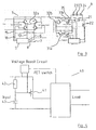
- a closed loop control for a high duty cycle power converter indicated generally by the reference numerals 1 and 2 respectively.
- the converter 2 comprises an input switching stage 3 and an output switching stage 4, only shown in outline.
- the closed loop control 1 is provided by a controller 5. The operation of the power converter is discussed in detail below.
- a measured duty cycle 6 of the power converter is fed into an averaging circuit 8 of the controller 5. Values analogous the measured duty cycle produced by the averaging circuit 8 are fed to an error amplifier 9 also connected to a desired duty cycle 7 which in turn provides a derived signal 11 to a logic circuit 10 in the controller 5.
- a variable signal 12 measured from the power converter 2 is also fed into the logic circuit 10.
- the derived signal 11 from the error amplifier 9 changes the variable signal 12 to provide a control signal 13 generated to an output driver circuit 14 which generates drive signals 15 and 16 to control the duty cycle of the power converter 2 and hence provide current mode control.
- An oscillator 17 controls the frequency at which the controller 5 generates the drive signals 15 and 16.
- controller 5 controls the duty cycle of the power converter 2 to provide closed loop current mode control as opposed to the output voltage of the converter 2 as normally is the case. Some variants are possible allowing the desired setting for the duty cycle to be dependent on, for example load current and/or input voltage of the converter 2.
- the measured duty cycle 6 is measured from the input stage of the power converter 2.
- the measured duty cycle 6 is obtained by measuring the conducting time interval of each switching element of the input switching stage 4, during a preset time interval which is normally expressed as a percentage value.
- the term "effective duty cycle" is the time when material current is flowing. While the input duty cycle is effectively fixed, this signal is modulated and changed to provide the effective duty cycle.
- This measured duty cycle 6 value is fed into an averaging circuit 8 to provide a signal analogous to the measured duty cycle 6.
- the desired duty cycle 7 is fed directly to the error amplifier 9. These two signals are compared by the error amplifier 9 to provide the derived signal 11 which is a function of the difference between the desired duty cycle 7 and the measured duty cycle 6.
- This derived signal 11 changes the variable signal 12 which implements current mode control to provide a control signal 13 which in turn provides drive signals 15, 16 to implement closed loop duty cycle control to maintain current mode control. It will be appreciated that if the desired duty cycle equals the measured duty cycle, then the error amplifier 9 provides a signal to the logic circuit 10 to provide current mode control and to provide stable output derived signals 15 and 16 to ensure closed loop duty cycle control is achieved.
- FIG. 2 there is illustrated an additional improvement of the present invention at the output switching stage 4 of the converter 2.
- a standard LC filter indicated by an inductor 21 and a capacitor 22 is connected between the switches of the power converter (not shown) to the output voltage.
- a diode 23 and a resistor 24 connected in series and in parallel with the inductor 21 clamps any deviating voltage to a level very close to the output voltage of the power converter.
- the resistor is preferably a controlled saturable resistor.
- the driving voltage is within 1 V, for example, of the output voltage and the diode 23 used in parallel with the output inductor 21 is a very effective and simple clamp.
- the diode 23 may comprise a number of diodes or a zener-diode type element or any other means to use the output of the power converter 2 to provide clamping.
- the stresses on the diode 23 during turn on can be very severe as effectively a voltage source at the input is being fed into the uncharged capacitor 22.
- the current limiting behaviour and leakage inductance's it may be necessary to place the resistor 24 in series with the diode 23. This involves a certain trade off in the clamping effectiveness.
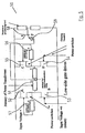
- Fig. 3 there is illustrated a detailed schematic of a typical power converter 2 having an input switching element 3 and an output switching element 4 incorporating the present invention.
- the operation of the switching elements are not discussed in detail as they do not form part of the present invention.
- Saturable reactors 31a and 31b are connected at the output switching stage 4 of the power converter 2.
- the saturable reactors 31a, 31b have the ability to adjust slightly the duty cycle to achieve removal of input ripple components of the converter 2. This requires an adjustment of the duty cycle, between 90% and 95% (or even as high as 99%) as illustrative values in the case of typical high duty cycle power converters, where the input ripple to the power converter would be the residual rectified mains/line voltage which would appear across the capacitor 22 in the power factor correction stage.
- the input ripple is 2-4% and is present at the output of the power factor correction stage, as well as correcting for voltage drops due to device losses.
- the effective duty cycle By adjusting the effective duty cycle by controlling the saturable reactors 31 a, 31b, the rectified input ripple is removed.
- a particularly suitable implementation of the present invention is the controlled saturable reactor 31a, 31b approach, but one envisages as alternatives the usage of auxiliary semi-conductor switching elements. Any suitable saturable magnetic element may also be used.
- a full-bridge output stage can also be configured based on the desired power level and transformer implementation.
- the diagonal pairs of input switches are driven alternately with a fixed drive waveform having a fixed deadtime or possibly adaptive depending on load or other parameters.
- the output switching elements are connected in series with the saturable magnetic elements, namely the reactors 31a, 31b which assist in bridge soft-switching but also whose reset condition can be controlled, giving a variable deadtime and thus adjustment of the effective duty cycle and output voltage.
- the range of control adjustment in practice will be determined by the desire to keep lossless switching conditions for the input switches over most load conditions, and this will be determined by the values of magnetising inductance and leakage inductance in the main power transformer shown (32a, 32b) and by any commutating inductance which may be placed in series with windings of this transformer (32a, 32b).
- Reset windings 35 and 36 are provided to operate under a control signal derived either from a closed loop monitoring of the output voltage or by a prediction of the needed ripple voltage requiring cancellation.
- Power converters of this type are designed for normal operation in conditions of continuous operation at high duty cycle. Such converters will typically perform poorly or exhibit conditions of high stresses on components if they are not operating at high duty cycle. It is thus important to derive approaches which control the behaviour of the circuit on start-up and in current limit conditions.
- a converter of this type may also be unsuited to gradual increase of the duty cycle as normally used in conventional power converters. If this type of converter is not used in association with a preregulator or postregulator, it may be necessary to use a linear dissipative regulator to control the turn-on and/or turn-off transition".
- a form of linear regulator control according to another aspect of the present invention, indicated by the reference numeral 40.
- the position is eased if the converter is preceded by a converter such as a buck type where the rate of voltage rise is relatively easily programmed.
- a boost pre-converter or fixed voltage source 41 does not however give this condition.
- the most cost-effective approach may often be to put a linear voltage-control circuit before such a converter. This is particularly the case if there is under voltage lockout protection on downstream circuitry such that minimal load current is drawn until the drop across the linear regulator.
- An example of such a linear regulator is shown in Fig. 4.
- the implementation is with an FET device 42 connected to a resistor 42 and capacitor 43 with an RC time constant determining the rate of rise and with the gate driven about the input supply rail in normal operation of the circuit.
- Other implementations of this circuit are possible, such as with the load converter being connected to the drain of the FET device 42.
- the invention is particularly effective for power converters having a high duty cycle.
- a non-isolated converter in cascade with a non-isolated converter to realise the overall power conversion function.
- the non-isolated converter is usually a simple buck converter with variable duty cycle and its combination with an isolated converter operating with near full duty cycle offer performance and cost advantages when compared with conventional approaches of using a variable duty cycle isolated converter.
- output rectifier for example, synchronous or diodes may be used.
- the present invention provides a power convert which can be cascaded with a non-isolated back or boost converter. This latter converter can act as a pre-regulator or post-regulator allowing the isolation stage to operate under optimal conditions with a rear fixed voltage transformation ratio.
- a high duty cycle power converter having a primary stage comprising either the push-pull, the half bridge or the full bridge configuration of a high duty cycle power converter, indicated generally by the reference numeral 50.
- the input stage 3 of the power converter 2 comprises a primary winding 51 of a transformer connected to input rectifying switches 52, 53, 54 and 55.
- Switches 54 and 55 have a separate auxiliary winding 56, 57 connected to the gate of switches 54 and 55.
- Each auxiliary winding 56, 57 is connected to the primary winding 51.
- This circuit has four switches as shown in Fig. 5, and is an implementation of particular value in this type of high duty cycle power converter.
- the switches 52-55 in the context of this high duty-cycle converter, are driven such that:
- this circuit operation will not automatically commence on start-up. It is possible to enter the mode of operation where both upper switches 52 and 55 are off and no drive voltage is generated across the auxiliary gate drive windings 56, 57. To address this issue, adding a clamp circuit 58, 59 is appropriate, and one implementation is shown. Here the mid-point of the main transformer primary winding 51 is connected to the clamp circuit 58, 59, which seeks to hold this point within a certain range of voltage typically centred around half the input voltage. The clamp voltage levels are determined by the resistors as shown.
- a transistor 58 is used to limit the extent to which the mid-point of the winding 51 can drop below one half of the input voltage. This means that as switch 53 is turned on, a voltage is developed across the transformer windings which rapidly turns on switch 53, and likewise if switch 54 is turned on, then switch 52 turns on. It will be appreciated that a significant current may be drawn from the transistor 58 but this is for a short time without any demanding high-frequency performance requirements. Thus, this device can be quite small. Diode 59 is provided to limit reverse stresses on transistor 58.
- transistor 58 may also be of value in effecting soft-start, where it is desired to gradually increase the output voltage.
- circuits are used with preregulators and it may be desired to pass a slowly-rising input voltage condition to the output as a slowly-rising output voltage. In these conditions, the voltage appearing across the input windings may be insufficient to turn on the high-side devices, and the transistor 58 provides the high-side current during this transition.
- switch 55 will remain on until such time as the voltage across the winding section is less than the threshold voltage of switch 55, in which case switch 55 will turn off. This asymmetric turn-off behaviour is inherent in the circuit and normally does not cause any issue.
- the gate drive windings may either be connected directly to the gate terminals of the "high side" of switches 52, 54, or they may be connected via resistors or other passive networks and/or transistors, these additional elements being used to optimise the drive waveform as applied to the gate terminals.
- switches 51-54 described above as FET devices or general transistors may be any type of gate-controlled switching device.
- the converter illustrated in Fig. 5, finds particular application in a near-full duty cycle small deadtime interval between conduction intervals of switches 54 and 55, converter with limited input voltage variation.
- Such a converter may be applied for example in association with a buck preregulator or immediately after a boost power factor conversion stage.
Landscapes
- Engineering & Computer Science (AREA)
- Power Engineering (AREA)
- Dc-Dc Converters (AREA)
- Amplifiers (AREA)
- Control Of Electric Motors In General (AREA)
- Control Of High-Frequency Heating Circuits (AREA)
- Emergency Protection Circuit Devices (AREA)
- Control Of Eletrric Generators (AREA)
Claims (22)
- Un convertisseur de puissance à cycle de service élevé (2) possédant une commande à mode de courant (1) à signal variable en boucle fermée (12) caractérisé par le fait qu'un signal variable (12) est modifié par un signal dérivé (11) qui est dérivé selon une fonction de la différence entre un cycle de service souhaité (7) et un cycle de service mesuré (6).
- Un convertisseur de puissance à cycle de service élevé (2) selon la Revendication 1, où le signal dérivé (11) est référencé avec le signal variable (12) pour fournir un signal de commande (13) dans un contrôleur (5) pour modifier le signal variable (12) afin d'actionner la commande à mode de courant
- Un convertisseur de puissance à cycle de service élevé (2) selon l'une quelconque des Revendications précédentes, comprenant un moyen de mesurer le cycle de service mesuré (6) à partir d'éléments de commutation de l'étage de commutation d'entrée (3) du convertisseur puissance (2) en mesurant l'intervalle temporel de fonctionnement actif de chaque élément de commutation pendant un intervalle temporel prédéfini.
- Un convertisseur de puissance à cycle de service élevé (2) selon l'une quelconque des Revendications précédentes, où le cycle de service souhaité est défini selon une condition de temps mon cohérente avec une commutation substantiellement sans pertes.
- Un convertisseur de puissance à cycle de service élevé (2) selon la Revendication 4, où le cycle de service souhaité est fixe dans la plage de 90 à 99%.
- Un convertisseur de puissance à cycle de service élevé (2) selon la Revendication 4, où un moyen est fourni de modifier le cycle de service souhait compte tenu de paramètres de fonctionnement.
- Un convertisseur de puissance à cycle de service élevé (2) selon la Revendication 6, où le paramètre de fonctionnement est la charge sur le convertisseur de puissance à cycle de service élevé (2).
- Un convertisseur de puissance à cycle de service élevé (2) selon l'une quelconque des Revendications précédentes, où un moyen est fourni de fournir un signal analogue aux cycles de service mesurés.
- Un convertisseur de puissance à cycle de service élevé (2) selon la Revendication 8, où le moyen comprend un circuit d'établissement de moyenne (8),
- Un convertisseur de puissance à cycle de service élevé (2) selon l'une quelconque des Revendications précédentes, où le contrôleur (5) comprend un amplificateur d'erreur (9) destiné à comparer le signal du cycle de service souhaité (7) au signal du cycle de service mesuré (6) pour fournir le signal dérivé (11).
- Un convertisseur de puissance à cycle de service élevé (2) selon l'une quelconque des Revendications précédentes, où le contrôleur (5) destiné à actionner la commande à mode de courant comprend un moyen de générer des signaux d'excitation (15, 16) à partir du signal de commande: (13) pour modifier le cycle de service des éléments de commutation d'entrée de l'étage de commutation d'entrée (3).
- Un convertisseur de puissance à cycle de service élevé (2) selon l'une quelconque des Revendications précédentes, où la sortie du convertisseur de puissance (2) est utilisée pour bloquer la tension du convertisseur de puissance (2).
- Un convertisseur de puissance à cycle de service élevé (2) selon la Revendication 12, où une diode (23) est connectée en parallèle à un inducteur de sortie (21) du convertisseur de puissance (2) pour bloquer la tension du convertisseur de puissance.
- Un convertisseur de puissance à cycle de service élevé (2) selon la Revendication 13, où une résistance (24) est placée en série la diode (23) et est connectée en parallèle avec l'inducteur de sortie (21).
- Un convertisseur de puissance à cycle de service élevé (2) selon l'une quelconque des Revendications précédentes, où il est fourni un moyen d'ajuster le cycle de service effectif pour compenser des tensions d'ondulation.
- Un convertisseur de puissance à cycle de service élevé (2) selon la Revendication 15, où il est fourni un réacteur saturable (31a, 31b) connecté aux éléments de commutation de sortie de l'étage de commutation de sortie (4) du convertisseur de puissance pour ajuster le cycle de service effectif du convertisseur de puissance (2).
- Un convertisseur de puissance à cycle de service élevé (2) selon la Revendication 16, où le réacteur saturable (31a, 31b) est fourni, avec une condition de réinitialisation commandable pour fournir un délai aux éléments de commutation de sortie pour ajuster le cycle de service effectif du convertisseur de puissance.
- Un convertisseur de puissance à cycle de service élevé (2) selon l'une quelconque des Revendications 15 à 17, comprenant un enroulement de réinitialisation possédant un signal de commande dérivé d'un contrôle en boucle fermée de la tension de sortie,
- Un convertisseur de puissance à cycle de service élevé (2) selon l'une quelconque des Revendications 15 à 17, où le moyen d'ajuster le cycle de service effectif comprend un enroulement de réinitialisation possédant un signal de commande obtenu à partir d'une prédiction de la tension d'ondulation nécessaire exigeant une annulation.
- Un convertisseur de puissance à cycle de service élevé (2) selon l'une quelconque des Revendications précédentes, où un enroulement auxiliaire distinct (56, 57) est connecté à l'enroulement principal (51) du convertisseur pour fournir un signal d'excitation de grille auxiliaire aux commutateurs (52, 55).
- Un convertisseur de puissance à cycle de service élevé (2) selon l'une quelconque des Revendications précédentes, où un circuit de blocage (58, 59) est connecté au point médian de l'enroulement principal (51).
- Un procédé de commande d'un convertisseur de puissance à cycle de service élevé (2) possédant une commande à mode de courant actionnée par un signal variable comprenant les opérations suivantes :mesurer (6) un cycle de service du convertisseur de puissance (2),comparer (9) un cycle de service souhaité (7) an cycle de service mesuré (6) pour fournir un signal dérivé (11),référencer (10) le signal dérivé (11) avec un signal de détection de courant (12) du convertisseur de puissance (2) pour fournir un signal de commande (13) : etgénérer des signaux d'excitation (15, 16) à partir du signal de commande (13) pour mettre en oeuvre une commande à mode de courant en boucle fermée (1) sur le convertisseur de puissance (2).
Applications Claiming Priority (3)
| Application Number | Priority Date | Filing Date | Title |
|---|---|---|---|
| IE20020224 | 2002-03-27 | ||
| IE20020224 | 2002-03-27 | ||
| PCT/IE2003/000049 WO2003081759A1 (fr) | 2002-03-27 | 2003-03-27 | Convertisseur de puissance |
Publications (2)
| Publication Number | Publication Date |
|---|---|
| EP1490959A1 EP1490959A1 (fr) | 2004-12-29 |
| EP1490959B1 true EP1490959B1 (fr) | 2007-10-31 |
Family
ID=28053194
Family Applications (1)
| Application Number | Title | Priority Date | Filing Date |
|---|---|---|---|
| EP03712613A Expired - Lifetime EP1490959B1 (fr) | 2002-03-27 | 2003-03-27 | Convertisseur de puissance |
Country Status (6)
| Country | Link |
|---|---|
| US (1) | US7277305B2 (fr) |
| EP (1) | EP1490959B1 (fr) |
| AT (1) | ATE377283T1 (fr) |
| AU (1) | AU2003216699A1 (fr) |
| DE (1) | DE60317176D1 (fr) |
| WO (1) | WO2003081759A1 (fr) |
Families Citing this family (4)
| Publication number | Priority date | Publication date | Assignee | Title |
|---|---|---|---|---|
| US7071660B2 (en) * | 2004-02-20 | 2006-07-04 | Virginia Tech Intellectual Properties, Inc. | Two-stage voltage regulators with adjustable intermediate bus voltage, adjustable switching frequency, and adjustable number of active phases |
| IE86922B1 (en) * | 2007-09-12 | 2018-09-05 | Texas Instruments Cork Ltd | A power converter |
| JP6287473B2 (ja) * | 2014-03-28 | 2018-03-07 | Tdk株式会社 | ブリッジレス力率改善コンバータ |
| US11165335B2 (en) | 2019-12-13 | 2021-11-02 | Semiconductor Components Industries, Llc | Non-regulated power converter with current sharing control |
Family Cites Families (21)
| Publication number | Priority date | Publication date | Assignee | Title |
|---|---|---|---|---|
| GB2075786B (en) * | 1980-03-21 | 1984-07-11 | Electrotech Instr Ltd | Switch mode converters |
| US5012139A (en) | 1989-10-30 | 1991-04-30 | Motorola Inc. | Full wave rectifier/averaging circuit |
| US5442540A (en) * | 1992-06-12 | 1995-08-15 | The Center For Innovative Technology | Soft-switching PWM converters |
| US5315498A (en) * | 1992-12-23 | 1994-05-24 | International Business Machines Corporation | Apparatus providing leading leg current sensing for control of full bridge power supply |
| JPH0746853A (ja) | 1993-07-29 | 1995-02-14 | Toshiba Corp | ソフトスイッチング式インバータ制御方法及びその装置 |
| JPH09191642A (ja) | 1996-01-10 | 1997-07-22 | Sanyo Denki Co Ltd | 直流電源装置 |
| JPH09229012A (ja) * | 1996-02-22 | 1997-09-02 | Honda Motor Co Ltd | パルス信号出力制御装置 |
| JP3141925B2 (ja) | 1996-08-30 | 2001-03-07 | サンケン電気株式会社 | ブリッジ型インバ−タ装置 |
| JPH11146648A (ja) * | 1997-11-06 | 1999-05-28 | Fuji Electric Co Ltd | 直流−直流変換装置 |
| JP3258620B2 (ja) | 1997-12-26 | 2002-02-18 | 東光株式会社 | スイッチング電源装置 |
| US5986904A (en) * | 1998-11-05 | 1999-11-16 | Lucent Technologies, Inc. | Self-regulating lossless snubber circuit |
| EP1095445A1 (fr) * | 1999-05-04 | 2001-05-02 | Koninklijke Philips Electronics N.V. | Convertisseur continu-continu |
| JP3535041B2 (ja) | 1999-05-28 | 2004-06-07 | 三菱電機株式会社 | Dc/dcコンバータ |
| US6282111B1 (en) * | 1999-06-18 | 2001-08-28 | Avionic Instruments Inc | Inverter control using current mode slope modulation |
| JP4694690B2 (ja) | 1999-12-16 | 2011-06-08 | 利康 鈴木 | 共振型ac−dcコンバーター装置 |
| JP2001211666A (ja) | 2000-01-25 | 2001-08-03 | Onkyo Corp | スイッチング電源回路 |
| JP2003527055A (ja) * | 2000-03-09 | 2003-09-09 | エコエアー コーポレーション | 交流発電機システム |
| JP3377499B2 (ja) | 2000-05-25 | 2003-02-17 | 長野日本無線株式会社 | スイッチング電源装置 |
| JP2002325458A (ja) | 2001-02-26 | 2002-11-08 | Shinei Sangyo Kk | 定電流装置 |
| JP2002272141A (ja) | 2001-03-09 | 2002-09-20 | Hitachi Metals Ltd | ブリッジ型コンバータ及びこれを用いたdc−dcコンバータ |
| JP4265112B2 (ja) | 2001-04-19 | 2009-05-20 | 横河電機株式会社 | スイッチングコンバータ |
-
2003
- 2003-03-27 EP EP03712613A patent/EP1490959B1/fr not_active Expired - Lifetime
- 2003-03-27 WO PCT/IE2003/000049 patent/WO2003081759A1/fr not_active Ceased
- 2003-03-27 US US10/509,027 patent/US7277305B2/en not_active Expired - Lifetime
- 2003-03-27 DE DE60317176T patent/DE60317176D1/de not_active Expired - Lifetime
- 2003-03-27 AT AT03712613T patent/ATE377283T1/de not_active IP Right Cessation
- 2003-03-27 AU AU2003216699A patent/AU2003216699A1/en not_active Abandoned
Also Published As
| Publication number | Publication date |
|---|---|
| US7277305B2 (en) | 2007-10-02 |
| DE60317176D1 (de) | 2007-12-13 |
| US20050231254A1 (en) | 2005-10-20 |
| WO2003081759A1 (fr) | 2003-10-02 |
| ATE377283T1 (de) | 2007-11-15 |
| EP1490959A1 (fr) | 2004-12-29 |
| AU2003216699A1 (en) | 2003-10-08 |
Similar Documents
| Publication | Publication Date | Title |
|---|---|---|
| US6618274B2 (en) | Synchronous rectifier controller to eliminate reverse current flow in a DC/DC converter output | |
| US5438498A (en) | Series resonant converter having a resonant snubber | |
| KR102613431B1 (ko) | 멀티 모드 스타트업을 갖는 스위칭 모드 파워 제어기 | |
| US6191957B1 (en) | Extended range boost converter circuit | |
| US6344986B1 (en) | Topology and control method for power factor correction | |
| Oruganti et al. | Soft-switched DC/DC converter with PWM control | |
| US5781419A (en) | Soft switching DC-to-DC converter with coupled inductors | |
| US5510974A (en) | High frequency push-pull converter with input power factor correction | |
| CN103296892B (zh) | 谐振变换器的多模工作和控制 | |
| US5894412A (en) | System with open-loop DC-DC converter stage | |
| JP4844674B2 (ja) | スイッチング電源装置 | |
| US7019988B2 (en) | Switching-type power converter | |
| US7778048B2 (en) | Switching power supply apparatus | |
| KR101811740B1 (ko) | 직렬 공진 컨버터에 대한 하이브리드 제어 기술 | |
| EP3393027A1 (fr) | Commutation souple pour conversion de puissance haute fréquence | |
| US20090284991A1 (en) | Switching power supply | |
| US20070081364A1 (en) | Highly efficient isolated AC/DC power conversion technique | |
| EP1126593A2 (fr) | Régulateur destiné au réglage d'une alimentation de puissance et son procédé de fonctionnement | |
| US6320764B1 (en) | Regulation circuit for a power converter and method of operation thereof | |
| US6151231A (en) | Circuit and method for reactive energy recirculation control in a series-resonant converter | |
| CN113632354B (zh) | 谐振转换器的软启动 | |
| EP1813012B1 (fr) | Convertisseur ca-cc | |
| US20220060120A1 (en) | Dynamic transient control in resonant converters | |
| US11075582B2 (en) | Switching converter | |
| WO2006095327A2 (fr) | Convertisseur de courant en mode commute et son procede de fonctionnement |
Legal Events
| Date | Code | Title | Description |
|---|---|---|---|
| PUAI | Public reference made under article 153(3) epc to a published international application that has entered the european phase |
Free format text: ORIGINAL CODE: 0009012 |
|
| AK | Designated contracting states |
Kind code of ref document: A1 Designated state(s): AT BE BG CH CY CZ DE DK EE ES FI FR GB GR HU IE IT LI LU MC NL PT RO SE SI SK TR |
|
| AX | Request for extension of the european patent |
Extension state: AL LT LV MK |
|
| 17P | Request for examination filed |
Effective date: 20041004 |
|
| 17Q | First examination report despatched |
Effective date: 20050121 |
|
| GRAP | Despatch of communication of intention to grant a patent |
Free format text: ORIGINAL CODE: EPIDOSNIGR1 |
|
| GRAS | Grant fee paid |
Free format text: ORIGINAL CODE: EPIDOSNIGR3 |
|
| GRAL | Information related to payment of fee for publishing/printing deleted |
Free format text: ORIGINAL CODE: EPIDOSDIGR3 |
|
| GRAS | Grant fee paid |
Free format text: ORIGINAL CODE: EPIDOSNIGR3 |
|
| GRAA | (expected) grant |
Free format text: ORIGINAL CODE: 0009210 |
|
| AK | Designated contracting states |
Kind code of ref document: B1 Designated state(s): AT BE BG CH CY CZ DE DK EE ES FI FR GB GR HU IE IT LI LU MC NL PT RO SE SI SK TR |
|
| REG | Reference to a national code |
Ref country code: GB Ref legal event code: FG4D |
|
| REG | Reference to a national code |
Ref country code: IE Ref legal event code: FG4D |
|
| REG | Reference to a national code |
Ref country code: CH Ref legal event code: EP |
|
| REF | Corresponds to: |
Ref document number: 60317176 Country of ref document: DE Date of ref document: 20071213 Kind code of ref document: P |
|
| NLV1 | Nl: lapsed or annulled due to failure to fulfill the requirements of art. 29p and 29m of the patents act | ||
| PG25 | Lapsed in a contracting state [announced via postgrant information from national office to epo] |
Ref country code: SE Free format text: LAPSE BECAUSE OF FAILURE TO SUBMIT A TRANSLATION OF THE DESCRIPTION OR TO PAY THE FEE WITHIN THE PRESCRIBED TIME-LIMIT Effective date: 20080131 Ref country code: CH Free format text: LAPSE BECAUSE OF FAILURE TO SUBMIT A TRANSLATION OF THE DESCRIPTION OR TO PAY THE FEE WITHIN THE PRESCRIBED TIME-LIMIT Effective date: 20071031 Ref country code: ES Free format text: LAPSE BECAUSE OF FAILURE TO SUBMIT A TRANSLATION OF THE DESCRIPTION OR TO PAY THE FEE WITHIN THE PRESCRIBED TIME-LIMIT Effective date: 20080211 Ref country code: NL Free format text: LAPSE BECAUSE OF FAILURE TO SUBMIT A TRANSLATION OF THE DESCRIPTION OR TO PAY THE FEE WITHIN THE PRESCRIBED TIME-LIMIT Effective date: 20071031 Ref country code: LI Free format text: LAPSE BECAUSE OF FAILURE TO SUBMIT A TRANSLATION OF THE DESCRIPTION OR TO PAY THE FEE WITHIN THE PRESCRIBED TIME-LIMIT Effective date: 20071031 |
|
| REG | Reference to a national code |
Ref country code: CH Ref legal event code: PL |
|
| PG25 | Lapsed in a contracting state [announced via postgrant information from national office to epo] |
Ref country code: BG Free format text: LAPSE BECAUSE OF FAILURE TO SUBMIT A TRANSLATION OF THE DESCRIPTION OR TO PAY THE FEE WITHIN THE PRESCRIBED TIME-LIMIT Effective date: 20080131 Ref country code: SI Free format text: LAPSE BECAUSE OF FAILURE TO SUBMIT A TRANSLATION OF THE DESCRIPTION OR TO PAY THE FEE WITHIN THE PRESCRIBED TIME-LIMIT Effective date: 20071031 Ref country code: PT Free format text: LAPSE BECAUSE OF FAILURE TO SUBMIT A TRANSLATION OF THE DESCRIPTION OR TO PAY THE FEE WITHIN THE PRESCRIBED TIME-LIMIT Effective date: 20080331 |
|
| PG25 | Lapsed in a contracting state [announced via postgrant information from national office to epo] |
Ref country code: AT Free format text: LAPSE BECAUSE OF FAILURE TO SUBMIT A TRANSLATION OF THE DESCRIPTION OR TO PAY THE FEE WITHIN THE PRESCRIBED TIME-LIMIT Effective date: 20071031 |
|
| PG25 | Lapsed in a contracting state [announced via postgrant information from national office to epo] |
Ref country code: DK Free format text: LAPSE BECAUSE OF FAILURE TO SUBMIT A TRANSLATION OF THE DESCRIPTION OR TO PAY THE FEE WITHIN THE PRESCRIBED TIME-LIMIT Effective date: 20071031 Ref country code: CZ Free format text: LAPSE BECAUSE OF FAILURE TO SUBMIT A TRANSLATION OF THE DESCRIPTION OR TO PAY THE FEE WITHIN THE PRESCRIBED TIME-LIMIT Effective date: 20071031 |
|
| EN | Fr: translation not filed | ||
| PG25 | Lapsed in a contracting state [announced via postgrant information from national office to epo] |
Ref country code: BE Free format text: LAPSE BECAUSE OF FAILURE TO SUBMIT A TRANSLATION OF THE DESCRIPTION OR TO PAY THE FEE WITHIN THE PRESCRIBED TIME-LIMIT Effective date: 20071031 Ref country code: RO Free format text: LAPSE BECAUSE OF FAILURE TO SUBMIT A TRANSLATION OF THE DESCRIPTION OR TO PAY THE FEE WITHIN THE PRESCRIBED TIME-LIMIT Effective date: 20071031 Ref country code: SK Free format text: LAPSE BECAUSE OF FAILURE TO SUBMIT A TRANSLATION OF THE DESCRIPTION OR TO PAY THE FEE WITHIN THE PRESCRIBED TIME-LIMIT Effective date: 20071031 |
|
| PLBE | No opposition filed within time limit |
Free format text: ORIGINAL CODE: 0009261 |
|
| STAA | Information on the status of an ep patent application or granted ep patent |
Free format text: STATUS: NO OPPOSITION FILED WITHIN TIME LIMIT |
|
| 26N | No opposition filed |
Effective date: 20080801 |
|
| PG25 | Lapsed in a contracting state [announced via postgrant information from national office to epo] |
Ref country code: DE Free format text: LAPSE BECAUSE OF FAILURE TO SUBMIT A TRANSLATION OF THE DESCRIPTION OR TO PAY THE FEE WITHIN THE PRESCRIBED TIME-LIMIT Effective date: 20080201 Ref country code: FR Free format text: LAPSE BECAUSE OF FAILURE TO SUBMIT A TRANSLATION OF THE DESCRIPTION OR TO PAY THE FEE WITHIN THE PRESCRIBED TIME-LIMIT Effective date: 20080704 Ref country code: MC Free format text: LAPSE BECAUSE OF NON-PAYMENT OF DUE FEES Effective date: 20080331 |
|
| PG25 | Lapsed in a contracting state [announced via postgrant information from national office to epo] |
Ref country code: GR Free format text: LAPSE BECAUSE OF FAILURE TO SUBMIT A TRANSLATION OF THE DESCRIPTION OR TO PAY THE FEE WITHIN THE PRESCRIBED TIME-LIMIT Effective date: 20080201 Ref country code: IE Free format text: LAPSE BECAUSE OF NON-PAYMENT OF DUE FEES Effective date: 20080327 Ref country code: EE Free format text: LAPSE BECAUSE OF FAILURE TO SUBMIT A TRANSLATION OF THE DESCRIPTION OR TO PAY THE FEE WITHIN THE PRESCRIBED TIME-LIMIT Effective date: 20071031 |
|
| PG25 | Lapsed in a contracting state [announced via postgrant information from national office to epo] |
Ref country code: FI Free format text: LAPSE BECAUSE OF FAILURE TO SUBMIT A TRANSLATION OF THE DESCRIPTION OR TO PAY THE FEE WITHIN THE PRESCRIBED TIME-LIMIT Effective date: 20071031 |
|
| PG25 | Lapsed in a contracting state [announced via postgrant information from national office to epo] |
Ref country code: CY Free format text: LAPSE BECAUSE OF FAILURE TO SUBMIT A TRANSLATION OF THE DESCRIPTION OR TO PAY THE FEE WITHIN THE PRESCRIBED TIME-LIMIT Effective date: 20071031 |
|
| PG25 | Lapsed in a contracting state [announced via postgrant information from national office to epo] |
Ref country code: HU Free format text: LAPSE BECAUSE OF FAILURE TO SUBMIT A TRANSLATION OF THE DESCRIPTION OR TO PAY THE FEE WITHIN THE PRESCRIBED TIME-LIMIT Effective date: 20080501 Ref country code: LU Free format text: LAPSE BECAUSE OF NON-PAYMENT OF DUE FEES Effective date: 20080327 |
|
| PG25 | Lapsed in a contracting state [announced via postgrant information from national office to epo] |
Ref country code: TR Free format text: LAPSE BECAUSE OF FAILURE TO SUBMIT A TRANSLATION OF THE DESCRIPTION OR TO PAY THE FEE WITHIN THE PRESCRIBED TIME-LIMIT Effective date: 20071031 |
|
| PG25 | Lapsed in a contracting state [announced via postgrant information from national office to epo] |
Ref country code: IT Free format text: LAPSE BECAUSE OF NON-PAYMENT OF DUE FEES Effective date: 20080331 |
|
| PGFP | Annual fee paid to national office [announced via postgrant information from national office to epo] |
Ref country code: GB Payment date: 20180223 Year of fee payment: 16 |
|
| GBPC | Gb: european patent ceased through non-payment of renewal fee |
Effective date: 20190327 |
|
| PG25 | Lapsed in a contracting state [announced via postgrant information from national office to epo] |
Ref country code: GB Free format text: LAPSE BECAUSE OF NON-PAYMENT OF DUE FEES Effective date: 20190327 |