EP1492120A2 - Circuit de temporisation, dispositif et système intégré à semiconducteurs auxquels le circuit de temporisation est connecté, et système de transmission de signaux - Google Patents
Circuit de temporisation, dispositif et système intégré à semiconducteurs auxquels le circuit de temporisation est connecté, et système de transmission de signaux Download PDFInfo
- Publication number
- EP1492120A2 EP1492120A2 EP04014102A EP04014102A EP1492120A2 EP 1492120 A2 EP1492120 A2 EP 1492120A2 EP 04014102 A EP04014102 A EP 04014102A EP 04014102 A EP04014102 A EP 04014102A EP 1492120 A2 EP1492120 A2 EP 1492120A2
- Authority
- EP
- European Patent Office
- Prior art keywords
- circuit
- signal
- timing
- clock
- output
- Prior art date
- Legal status (The legal status is an assumption and is not a legal conclusion. Google has not performed a legal analysis and makes no representation as to the accuracy of the status listed.)
- Granted
Links
Images






























Classifications
-
- G—PHYSICS
- G11—INFORMATION STORAGE
- G11C—STATIC STORES
- G11C11/00—Digital stores characterised by the use of particular electric or magnetic storage elements; Storage elements therefor
- G11C11/21—Digital stores characterised by the use of particular electric or magnetic storage elements; Storage elements therefor using electric elements
- G11C11/34—Digital stores characterised by the use of particular electric or magnetic storage elements; Storage elements therefor using electric elements using semiconductor devices
- G11C11/40—Digital stores characterised by the use of particular electric or magnetic storage elements; Storage elements therefor using electric elements using semiconductor devices using transistors
- G11C11/401—Digital stores characterised by the use of particular electric or magnetic storage elements; Storage elements therefor using electric elements using semiconductor devices using transistors forming cells needing refreshing or charge regeneration, i.e. dynamic cells
- G11C11/4063—Auxiliary circuits, e.g. for addressing, decoding, driving, writing, sensing or timing
- G11C11/407—Auxiliary circuits, e.g. for addressing, decoding, driving, writing, sensing or timing for memory cells of the field-effect type
-
- H—ELECTRICITY
- H04—ELECTRIC COMMUNICATION TECHNIQUE
- H04L—TRANSMISSION OF DIGITAL INFORMATION, e.g. TELEGRAPHIC COMMUNICATION
- H04L7/00—Arrangements for synchronising receiver with transmitter
- H04L7/02—Speed or phase control by the received code signals, the signals containing no special synchronisation information
- H04L7/033—Speed or phase control by the received code signals, the signals containing no special synchronisation information using the transitions of the received signal to control the phase of the synchronising-signal-generating means, e.g. using a phase-locked loop
- H04L7/0337—Selecting between two or more discretely delayed clocks or selecting between two or more discretely delayed received code signals
-
- G—PHYSICS
- G11—INFORMATION STORAGE
- G11C—STATIC STORES
- G11C11/00—Digital stores characterised by the use of particular electric or magnetic storage elements; Storage elements therefor
- G11C11/21—Digital stores characterised by the use of particular electric or magnetic storage elements; Storage elements therefor using electric elements
- G11C11/34—Digital stores characterised by the use of particular electric or magnetic storage elements; Storage elements therefor using electric elements using semiconductor devices
- G11C11/40—Digital stores characterised by the use of particular electric or magnetic storage elements; Storage elements therefor using electric elements using semiconductor devices using transistors
- G11C11/401—Digital stores characterised by the use of particular electric or magnetic storage elements; Storage elements therefor using electric elements using semiconductor devices using transistors forming cells needing refreshing or charge regeneration, i.e. dynamic cells
- G11C11/4063—Auxiliary circuits, e.g. for addressing, decoding, driving, writing, sensing or timing
- G11C11/407—Auxiliary circuits, e.g. for addressing, decoding, driving, writing, sensing or timing for memory cells of the field-effect type
- G11C11/4076—Timing circuits
-
- G—PHYSICS
- G11—INFORMATION STORAGE
- G11C—STATIC STORES
- G11C7/00—Arrangements for writing information into, or reading information out from, a digital store
- G11C7/10—Input/output [I/O] data interface arrangements, e.g. I/O data control circuits, I/O data buffers
- G11C7/1072—Input/output [I/O] data interface arrangements, e.g. I/O data control circuits, I/O data buffers for memories with random access ports synchronised on clock signal pulse trains, e.g. synchronous memories, self timed memories
-
- G—PHYSICS
- G11—INFORMATION STORAGE
- G11C—STATIC STORES
- G11C7/00—Arrangements for writing information into, or reading information out from, a digital store
- G11C7/22—Read-write [R-W] timing or clocking circuits; Read-write [R-W] control signal generators or management
-
- G—PHYSICS
- G11—INFORMATION STORAGE
- G11C—STATIC STORES
- G11C7/00—Arrangements for writing information into, or reading information out from, a digital store
- G11C7/22—Read-write [R-W] timing or clocking circuits; Read-write [R-W] control signal generators or management
- G11C7/222—Clock generating, synchronizing or distributing circuits within memory device
-
- G—PHYSICS
- G11—INFORMATION STORAGE
- G11C—STATIC STORES
- G11C8/00—Arrangements for selecting an address in a digital store
- G11C8/18—Address timing or clocking circuits; Address control signal generation or management, e.g. for row address strobe [RAS] or column address strobe [CAS] signals
-
- H—ELECTRICITY
- H04—ELECTRIC COMMUNICATION TECHNIQUE
- H04L—TRANSMISSION OF DIGITAL INFORMATION, e.g. TELEGRAPHIC COMMUNICATION
- H04L7/00—Arrangements for synchronising receiver with transmitter
- H04L7/0016—Arrangements for synchronising receiver with transmitter correction of synchronization errors
- H04L7/002—Arrangements for synchronising receiver with transmitter correction of synchronization errors correction by interpolation
- H04L7/0025—Arrangements for synchronising receiver with transmitter correction of synchronization errors correction by interpolation interpolation of clock signal
-
- H—ELECTRICITY
- H03—ELECTRONIC CIRCUITRY
- H03K—PULSE TECHNIQUE
- H03K5/00—Manipulating of pulses not covered by one of the other main groups of this subclass
- H03K2005/00013—Delay, i.e. output pulse is delayed after input pulse and pulse length of output pulse is dependent on pulse length of input pulse
- H03K2005/00019—Variable delay
- H03K2005/00026—Variable delay controlled by an analog electrical signal, e.g. obtained after conversion by a D/A converter
- H03K2005/00052—Variable delay controlled by an analog electrical signal, e.g. obtained after conversion by a D/A converter by mixing the outputs of fixed delayed signals with each other or with the input signal
Definitions
- the current value control unit may control the current value of the current source by an output of a D/A converter.
- the analog/digital converting unit may be a comparator for comparing the summed waveform with a reference level for conversion into a digital waveform.
- the weighting control unit may include a current-output D/A converter, and an output of the D/A converter may be controlled by being switched for connection to either a capacitive-coupled terminal or its complementary terminal.
- the weighting control unit may be configured to vary the number of current sources to be connected to a load capacitance terminal.
- the weighting control unit may include a clamp circuit for holding a terminal voltage level within a fixed range.
- the phase interpolator may be configured so that the size of transistors to be switched and the quantization step size of a D/A converter are made variable to provide a desired linearity characteristic to a timing output versus a control signal.
- the row address strobe signal /RAS makes a transition to a low level "L"
- the following series of RAS-related operations is performed asynchronously with the clock CLKi. That is, the high-order part of the address, A23 - A12, is latched into a row address buffer register 7 by a signal from the timing signal generating circuit 2 and is decoded by a row decoder 8.
- Selected word line WL is raised to a high voltage by a signal RX from the timing signal generating circuit 2, and charge in a cell 6a is read out onto the bit line BL.
- timings for signal activation and deactivation are adjusting in the timing signal generating circuit 2 by utilizing signal delays through loads such as transistors, capacitors, wiring, etc. regardless of whether the DRAM is a clock synchronous DRAM or asynchronous DRAM.
- the design for such timing adjustments is performed using simulation, to accomplish the timing adjustments with high accuracy, but since variations in manufacturing process, fluctuations in supply voltage, etc. must be considered, the design time becomes longer and the cost increases accordingly.
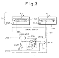
- the logic circuits 24 and 25 operate synchronously with the clock CLKi.
- the logic circuit 24 supplies a chip select signal /CS, a row address strobe signal /RAS, a column address strobe signal /CAS, and a write enable signal /WE to the command decoder 1, and a command appropriate to the combination of the logic values of these signals at the rising of the clock CLKi, for example, is issued from the command decoder 1.
- the command is SANC, SAPC, PRC, or PXC corresponding to the earlier mentioned SAN, SAP, PR, or PX, respectively.
- an arbitrary one of these commands is designated CNTC and the DRAM control signal corresponding to the command CNTC is designated CNT.
- the loop counter 282 After being initialized by the reset pulse RST, the loop counter 282 is set to "01...0" by application of two pulses of the clock ⁇ 4, which causes the pMOS transistor 33B to turn on, and the output of the flip-flop 30 thus goes to the low level "L".
- clocks with prescribed phases output from the multi-phase clock generating circuit 26 are counted by the counters to adjust the timing for the activation and deactivation of the control command CNTC, that is, since the timing is adjusted (in a digital manner) in units of integral multiples of the number of delay stages in the multi-phase clock generating circuit 26, there is no need to strictly consider manufacturing process variations and supply voltage fluctuations in timing design.
- the bit length must be made long enough that the contents of the loop counters 281 and 282 do not make a complete cycle around the loop within a RAS cycle that starts at the fall of the row address strobe signal /RAS and ends at the next fall thereof.
- the loop counter 281 counts the clock CLKi, and the clock ⁇ 3 and a predetermined bit output of the loop counter 281 are supplied to an AND gate 37 to create the activation timing signal CNT1, while the clock ⁇ 4 and a predetermined bit output of the loop counter 281 are supplied to an AND gate 38 to create the deactivation timing signal CNT2.
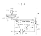
- the AND gate 36 in Figure 5 is eliminated and, instead, an AND gate 283 is used in the counter circuit 28B, and the clock CLKi and the control command CNTC are supplied to the AND gate 283 whose output is then counted by the loop counter 281.
- the output of the flip-flop 30 can be used directly as the control signal CNT, and there is no need to consider the delay associated with the AND gate 36 in Figure 5. Furthermore, since the CLKi is passed through the AND gate 283 and counted by the loop counter 281 only when the control command CNTC is at a high level "H", the power consumption of the counter circuit 28B can be reduced.
- the AND gate 36 in Figure 5 is eliminated, and instead, an AND gate 1a is provided in the command decoder 1A, and an output of the loop counter 281 and the control command CNTC are supplied to the AND gate 1a.
- the AND gate 1a and the command decoder 1 in Figure 2 together constitute the command decoder 1A.
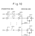
- Figure 10 is a block circuit diagram showing in schematic form one example of the prior art signal transmission system.
- reference numeral 401 is a drive circuit (buffer) for a clock clk at the transmitting end
- 411 to 41n are drive circuits for data DD1 to DDn at the transmitting end
- 402 is a clock line (clock signal line)
- 421 to 42n are data lines (data signal lines)
- 403 is a drive circuit for the clock at the receiving end
- 431 to 43n are drive circuits for the data at the receiving end
- 441 to 44n are data latch circuits (input latches).
- reference numerals 511 to 51n are drive circuits (drivers) for data DD1 to DDn at the transmitting end
- 521 to 52n are data lines (data signal lines)
- 531 to 53n are timing adjusting circuits (optimum timing determining means)
- 541 to 54n are data latch circuits (input latches).
- the timing adjusting circuits 531 to 53n are also supplied with the clock clk, and the signal latch timing at each of the input latches (receiving circuits) 541 to 54n is optimized according to the skew on each of the signal lines 521 to 52n.
- the timing adjusting circuits 531 to 53n are configured to output strobe signals (clocks), clk1 to clkn, near the center of the period (data window) during which the data DD1 to DDn are valid.
- the rise timing of the strobe signal clk1 substantially coincides with the center of the period during which the data DD1 is valid; the rise timing of the strobe signal clk2 substantially coincides with the center of the period during which the data DD2 is valid; and the rise timing of the strobe signal clkn substantially coincides with the center of the period during which the data DDn is valid.
- the timing adjusting circuits 531 to 53n are not limited to the illustrated configuration where the timing of the strobe signals clk1 to clkn supplied to the respective timing adjusting circuits 531 to 53n is adjusted at the receiving end; for example, the configuration may be such that the timing of the data DD1 to DDn is adjusted at the transmitting end.
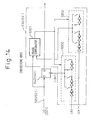
- reference numeral 530 is a timing adjusting circuit (optimum timing determining means)
- 5301 is a phase comparator circuit
- 5302 and 5303 are variable delay circuits
- 540 is a data latch circuit (input latch)
- 520 is a signal line (data signal line).
- the variable delay circuits 5302 and 5303 are identical in configuration, and provide the same amount of delay in accordance with an output from the phase comparator circuit 5301.
- the data DD, signal line 520, timing adjusting circuit 530, and input latch 540 in the first embodiment correspond, for example, to the data DD1, signal line 521, timing adjusting circuit 531, and input latch 541 in Figure 11; therefore, the circuit block shown here is provided for each of the data (DD1 to DDn).
- the timing adjusting circuit 530 for adjusting the relative timing relationship between the received signal (data) DD and the clock clk (clk') is provided at the receiving end so that the input latch 540 latches the data DD at the optimum timing (the timing near the center of the period during which the data DD is valid). More specifically, as shown in Figure 14, the timing adjusting circuit 530 comprises the first variable delay circuit 5302 which provides a delay to the first clock clk, the second variable delay circuit 5303 which provides a delay to the second clock clk', and the phase comparator circuit 5301 which compares the phase of the data DD with the phase of the second clock clk' supplied via the second variable delay circuit 5303.
- the rise timing of the first clock clk having a 180-degree phase difference relative to the second clock clk' is made to substantially coincide with the timing at the center of the period (data window) during the data DD is valid, thus achieving data reception with low error rates.
- the modified example (timing adjusting circuit 530') of the first embodiment can be applied when the clock (clk0) has a duty cycle of about 50%, that is, the high level period of the clock clk0 is approximately equal in length to the low level period thereof.
- the clock clk0 is used as the second clock clk' in Figure 14, and the first clock clk and the first variable delay circuit 5302 in Figure 14 can be eliminated.
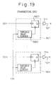
- FIG 19 is a block diagram showing in schematic form a third embodiment of the signal transmission system according to the second aspect of the present invention.
- reference numerals 561 to 56n are timing adjusting circuits (optimum timing determining means)
- 5601 is a data latch circuit (output latch)
- 5602 is a variable delay circuit.
- the signal transmission system of the third embodiment accomplishes timing adjustments at the signal transmitting end by making transmission timing variable.
- the output latch 5601 is provided in front of each of the transmitting drive circuits (drivers) 511 to 51n, and the clock clk delayed through the variable delay circuit 5602 is used as the strobe signal to the output latch 5601. That is, the timing of each of the drivers 511 to 51n is adjusted by the output of the variable delay circuit 5602 whose amount of delay is controlled in a variable manner.
- the timing adjusting circuit 561 controls the driver 511 so that the data DD1 is transmitted at such a timing that the clock at the receiving end occurs at the optimum point of the data DD1 (the timing that substantially coincides with the center of the period during which the data DD is valid).
- the transmission timing of the data (DD1 to DDn) is adjusted by the timing adjusting circuit (561 to 56n) at the transmitting end, and this timing adjustment is performed using a communication protocol, for example, when power is turned on.
- the signal transmission system of the third embodiment can simplify the circuit configuration at the receiving end, and is preferred, for example, when cost reductions of receiving devices are strongly desired.
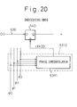
- Figure 20 is a block circuit diagram showing in schematic form a fourth embodiment of the signal transmission system according to the second aspect of the present invention.
- reference numeral 5310 is a timing adjusting circuit
- 5311 is a phase interpolator.
- the timing adjusting circuit 5130 comprises the phase interpolator 5311 which generates from a plurality of clocks with different phases a new clock having an intermediate phase. More specifically, four-phase clocks ⁇ 0 to ⁇ 3 are supplied to the phase interpolator 5311 and, based on these four-phase clocks, an intermediate phase is generated and the resulting strobe signal (clk00) is supplied to the input buffer 540. Needless to say, this phase interpolator 5311 is provided for each input latch 540 (541 to 54n) which latches the data DD (DD1 to DDn) transmitted via each signal line 520 (521 to 52n).
- Figure 21 is a circuit diagram showing one example of the phase interpolator in the signal transmission system of Figure 20.
- the phase interpolator 5311 takes a weighted sum of the four-phase input clocks ⁇ 0 to ⁇ 3 by varying the tail current of a pair of differential amplifier stages 5312 and 5313, and supplies signals S1 and S2 from the two differential amplifier stages 5312 and 5313 to a comparator 5313 to obtain an output (strobe signal clk00) having a phase intermediate between the phases of these two signals S1 and S2.
- weighting of the input clocks ⁇ 0 to ⁇ 3 in the differential amplifier stages 5312 and 5313 is done using a plurality of control transistor pairs each consisting, for example, of two nMOS transistors connected in series.
- FIG 22 is a block circuit diagram showing in schematic form a fifth embodiment of the signal transmission system according to the second aspect of the present invention.
- reference numeral 570 is a retiming circuit
- 571 to 573 are latch circuits
- 574 is a selector
- 575 is a shift register
- 576 is a variable delay circuit
- 577 is a delay control circuit.
- the fifth embodiment is applied to the case where the variable delay circuit 576 is inserted in the path of the clock (strobe signal) used to drive the input latch 540 at the receiving end.
- the variable delay circuit 576 and delay control circuit 577 shown here correspond, for example, to the variable delay circuit 5302 and phase comparator circuit 5301 in the first embodiment shown in Figure 14.
- variable delay circuit 576 (5302) is inserted in the path of the clock to the input latch 540 to enable the data DD to be latched at the optimum timing, but as for the signal passed through the input latch 540, though the signal level is digitized, the data change timing is different for each signal line (data line) 520 because of the skew on the cable.
- the retiming circuit 570 comprises the latch circuits 571 to 573 and selector 574; either the output of the two-stage cascaded latch circuits 571 and 572 or the output of the latch circuit 573 is selected by the selector 574.
- a strobe signal RTB is supplied to the latch circuit 571, and a strobe signal RTA to the latch circuits 572 and 573.
- the strobe signal RTA has a phase difference of 180 degrees with respect to the strobe signal RTB.
- each data (signal) DD (DD1 to DDn) is latched at the optimum timing at the output position of the input latch 540 (541 to 54n) indicated by PT51 in Figure 22, the data change timing is different for each data DD (DD1 to DDn) because of the skew due to the signal line, etc.
- data latching is possible with the timing (rise timing) of at least one of the two signals (strobe signals), RTA and RTB, that are 180 degrees out of phase with respect to each other. More specifically, when the rise timing of one strobe signal RTA occurs in the transition region of the data DD2 and DDn, for example, the rise timing of the other strobe signal RTB, which is 180 degrees out of phase with respect to the signal RTA, invariably occurs during the period when the data DD2 and DDn are valid, and the data can thus be latched.
- the output of the input latch 540 is latched both by the latch circuit 571, to which the strobe signal RTB is supplied, and by the latch circuit 573, to which the strobe signal RTA is supplied, so that at least either one of the latch circuits can latch the correct data; further, with the provision of the latch circuit 572 following the latch circuit 571, the outputs of the latch circuits 571 (572) and 573 can be supplied to the selector 574 at the timing defined by the strobe signal RTA.
- the output of the delay control circuit 577 is supplied to the selector 574 to determine which of the two outputs, the latch circuit 572 or 573, is to be selected.
- the data DD1 to DDn change at the same timing (the data are retimed) at the output position of the selector 574 indicated by PT52 in Figure 22.
- a one-bit or a longer-than-one-bit delay may exist between the data DD1 to DDn.
- the shift register 575 is provided following the selector 574 to match (deskew) the output timing of all data to the timing of the data having the greatest delay (for example, the data DDn).
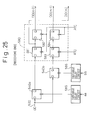
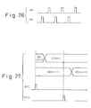
- Figure 25 is block circuit diagram showing in schematic form a sixth embodiment of the signal transmission system according to the second aspect of the present invention, and Figures 26 and 27 are timing diagrams for explaining one example of an operation in the signal transmission system of Figure 25.
- reference numeral 580 is a retiming circuit
- 581 to 584 are latch circuits
- 585 and 586 are variable delay circuits
- 540a and 540b are input latches.
- the frequency of the strobe signals aa and bb is twice the frequency of, for example, the signals RTA and RTB in the foregoing fifth embodiment, and the data DD (..., DD(m-2), DD(m-1), DD(m), DD(m+1), DD(m+2), ...) sequentially transmitted over the signal line 520 are latched alternately by the input latches 540a and 540b. Accordingly, the input latches 540a and 540b need only operate at half the speed of the actual data rate (the transmitted signal rate).
- the above interleaving operation is not limited to interleaving between two parts, but the interleaving may be performed between three or more parts.
- the signal transmission system of the sixth embodiment is suitable for high-speed transmission of signals. This also offers the advantage of simplifying the circuit design because time constrains are eased for latch operations in the retiming circuit 580.
- Figure 28 is a block diagram showing in schematic form a seventh embodiment of the signal transmission system according to the second aspect of the present invention, in which a so-called PRD (Partial Response Detection) type latch (differential PRD receiver) is used as the interleaving latch.
- PRD Partial Response Detection
- reference numerals 520a and 520b are signal lines for transmitting complementary signals (data) DD and /DD
- 590a and 590b are PRD amplifiers which operate in an interleaving fashion.
- the two signal lines 520a and 520b are provided for one data DD which is thus transmitted as complementary data DD and /DD. It will be appreciated that in other embodiments also, either a single line or differential (complementary) lines may be used for signal transmission.
- the receiver circuit (input latch) of the seventh embodiment comprises the first PRD amplifier 590a and second PRD amplifier 590b to which the complementary data DD and /DD are supplied, and which operate in interleaving fashion by being controlled by control signals ⁇ 10 and ⁇ 20.
- output signals from the first and second PRD amplifiers 590a and 590b are processed, for example, via a serial-parallel conversion circuit or the like, for a lower operating frequency at the subsequent stage.
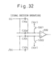
- Figure 29 is a circuit diagram showing one example of the PRD amplifier in the signal transmission system of Figure 28.
- reference numeral 591 is a PRD functional block
- 592 is a differential amplifier block having a precharge function
- 593 and 594 are a waveform shaping differential amplifier and inverter.
- the PRD functional block 591 comprises four capacitors C10a, C10b, C20a, and C20b, and four transfer gates (switch means) 5911, 5912, 5913, and 5914, and the connections of the capacitors are controlled by the control signals ⁇ 10 (/( ⁇ 10) and ⁇ 20 (/ ⁇ 20) so that the intersymbol interference component elimination operation and signal decision operation shown in Figures 31 and 32 are performed alternately.
- the differential amplifier block 592 differentially amplifies the input signals and makes a decision on the data. Further, the differential amplifier block 592 includes transfer gates 5921 and 5922 so that a precharge operation is performed during the intersymbol interference component estimation operation.
- the differential amplifier 593 and inverter 594 are provided to amplify the output level of the differential amplifier block 592 and output a waveshaped signal.
- complementary transfer gates are used as the switch devices, but other devices having switching functions can also be used; for example, the switch devices may be constructed using only NMOS transistors or only PMOS transfer gates.
- the differential amplifier block 592 is configured as an NMOS gate-receiving type, but whether it should be configured as an NMOS gate-receiving type or PMOS gate-receiving type depends on technology, etc., and whichever is suitable can be chosen.
- the receiver circuit of the seventh embodiment shown in Figure 28 performs interleaving operations such that, at one timing, one PRD amplifier (the first PRD amplifier 590a) performs an intersymbol interference component estimation operation while the other PRD amplifier (the second PRD amplifier 590b) is performing a data decision operation, and at the next timing, the one PRD amplifier (the first PRD amplifier 590a) performs a data decision operation while the other PRD amplifier (the second PRD amplifier 590b) is performing an intersymbol interference component estimation operation.
- precharging of the same PRD amplifier is being performed at the same time, and the input level is precharged to a prescribed voltage (precharge voltage Vpr) through the transfer gates 5921 and 5922. Since this precharging is performed in the background during the interleave data read period, the precharge time does not affect the data transfer cycle.
- FIG 33 is a block circuit diagram showing in schematic form an eighth embodiment of the signal transmission system according to the second aspect of the present invention.
- reference numeral 501 is a drive circuit (clock driver) for the clock clk at the transmitting end
- 502 is a clock line
- 503 is a clock receiver
- 611 to 61n are variable delay circuits (clock timing adjusting circuits).
- the timing of the transmitted clock clk is adjusted at the receiving end by the variable delay circuits 611 to 61n provided for the input latches 541 to 54n, to optimize data latching timing at the input latches 541 to 54n.
- the clock clk is sent from the transmitting end together with the data DD1 to DDn (the clock is sent as special data of a bit pattern repeating as "0101"); if there is jitter in the clock generating circuit at the transmitting end, the jitter is common to all transmitted data and clock clk. Accordingly, in the signal transmission system of the eighth embodiment, jitter causes no ill effect as long as the data are latched using this clock clk.
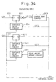
- Figure 34 is a block circuit diagram showing in schematic form a ninth embodiment of the signal transmission system according to the second aspect of the present invention.
- reference numerals 602 and 621 are latch circuits
- 603 is a charge pump circuit
- 604, 641, and 651 are variable delay circuits
- 661 is a delay amount memory circuit.
- the output of the latch circuit 602 is supplied to the charge pump circuit 603 via two stages of inverters.
- the clock clk is sent from the transmitting end together with the data DD1 (DD1 to DDn).
- This clock clk is latched by the input latch (latch) 602 identical in configuration to other data receiving latches; here, an internal clock clki passed through the variable delay circuit 604 is used as the strobe signal to latch the clock clk in the latch 602. That is, the clock used to drive the latch 602 is obtained by passing the reference clock (internal clock clki) at the receiving end through a variable delay stage (the variable delay circuit 604).
- the delay control signal DCS is also supplied to the variable delay circuit 641 to likewise control the clock timing of the input latch 621 for another data line in a variable manner; in this way, the jitter component simultaneously impressed on the clock clk and data DD1 can be eliminated, as in the foregoing eighth embodiment, preventing an ill effect from being caused to the output.
- the signal transmission system of the ninth embodiment has the advantages that the noise superimposed on the clock clk can be eliminated, and that there is no need to make special provision to match the phase shift at the clock receiving system with the phase at the data receiving system, since exactly the same laches 602 and 621 can be used for the reception of the clock clk and the data DD1 (DD1 to DDn).
- Figure 35 is a block circuit diagram showing in schematic form a modified example of the signal transmission system of Figure 34.
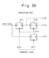
- Figure 36 is a block circuit diagram showing in schematic form a 10th embodiment of the signal transmission system according to the second aspect of the present invention. This embodiment is applicable, for example, to a coding scheme, such as 8B/10B, where the existence of a clock component in a data sequence is guaranteed.
- reference numerals 671 to 673 are latch circuits.
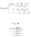
- Figure 37 is a timing diagram for explaining one example of operation in the signal transmission system of Figure 36
- Figure 38 is a diagram showing the relationship between the internal clock state and the output of each latch in the signal transmission system of Figure 36.
- Figure 38 shows the relationship of the output of the latch 671 (current data DB), the output of the latch 672 (immediately preceding data DA), and the output of the latch 673 (transient region data DT), relative to the internal clocks (strobe signals ( ⁇ 01 and ⁇ 02). That is, when DA, DT, DB are "0, 0, 1" or "1, 1, 0", this indicates that the internal clock ( ⁇ 01, ⁇ 02) is advanced, in which case the internal clock ( ⁇ 01, ⁇ 02) is delayed using, for example, the signal DN.
- a special period (calibration mode) is provided to adjust the latch timing for normal data; if the data is coded using 8B/10B code, for example, and the existence of a clock component in the data sequence is thus guaranteed, the adjustment work can be performed at all times during data reception (data transmission mode).
- FIG 39 is a timing diagram for explaining an 11th embodiment of the signal transmission system according to the second aspect of the present invention.
- the signal transmission system of the 11th embodiment employs, for example, a configuration similar to that of the eighth embodiment shown in Figure 33, and transmits from the transmitting end phase-adjusting data DDP (a bit sequence of 0101...) 180 degrees out of phase with respect to normal data and, at the receiving end, the clock clk is synchronized to the phase-adjusting data DDP.
- the amount of delay in the variable delay circuit is controlled so that the rise and fall timings of the clock clk each coincide with a data window boundary.
- Figure 39 shows the case of DDR (Double Data Rate), that is, an example of the case where data are latched at both the rise and fall timings of the clock clk. It will be appreciated that in other embodiments of the signal transmission system of the present invention, DDR can be applied so that data can be latched at both the rise and fall timings of the clock.
- DDR Double Data Rate
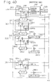
- Figures 40 and 41 are block circuit diagrams showing a 12th embodiment of the signal transmission system according to the second aspect of the present invention.
- reference numeral 680 is a DLL (Delay Locked Loop) circuit
- 681 is a latch block for the clock clk
- 682 is a control signal generating circuit
- 683 is an up-down counter (UDC)
- 684 is a phase interpolator (PIP)
- 685 is a clock generating circuit (CLKGE).
- the control signal generating circuit 682 outputs an up signal UP and down signal DN to the up-down counter 683 in accordance with the outputs of the latch circuits 681a and 681b, and the up-down counter 683 counts the up signal UP and down signal DN for feedback control of the phase interpolator 684, thereby controlling the timing of the strobe signals to the latch circuits 681a and 681b.
- the output of the up-down counter 683 is also supplied to the phase interpolators 6841 to 684n for the respective data DD1 to DDn, to control the latch timing at the latch circuits 6811a, 6811b to 681na, 681nb in the respective latch blocks 6811 to 681n.
- the initial value setting circuits 6871 to 687n provided for the respective data lines 521 to 52n, perform a phase adjusting test as a calibration mode, for example, when power is turned on, and store delay amounts for the respective signal lines; then, their initial values and the output of the up-down counter 683 are added together by the respective adder circuits 6861 to 686n, and the results are supplied to the respective phase interpolators 6841 to 684n which absorb phase variations between the respective signal lines at the initial condition to ensure that the data are latched correctly in the normal data transmission mode.
- a master clock (receiving clock) clkm is processed by the DLL circuit 680, and a four-phase clock obtained by dividing the frequency f of the clock clkm by 8 is supplied to each of the phase interpolators 684 and 6841 to 684n.
- the signal supplied from the up-down counter 683 to the phase interpolators 684 and 6841 to 684n and the initial values stored in the initial value setting circuits 6871 to 687n are, for example, 6-bit signals.
- the up-down counter 683 here corresponds, for example, to the charge pump 603 in the ninth embodiment shown in Figure 34. However, while the charge pump 603 in the ninth embodiment processes the phase information of the clock in an analog manner, the up-down counter 683 in the 12th embodiment differs in that the clock phase information is processed as a digital value.
- the outputs of the phase interpolator 684 are supplied to the retiming circuits 6881 to 688n as well as to the clock generating circuit 685 which generates a clock clkc for logic circuitry.
- the retiming circuit 6881 (6881 to 688n) comprises three latch circuits 6881a, 6881b, and 6881c; the same strobe signal as supplied to the latch circuit 681a in the clock latch block 681 is supplied to the latch circuit 6881a, while the same strobe signal as supplied to the latch circuit 681b in the clock latch block 681 is supplied to the latch circuits 6881b and 6881c.
- the retiming circuits 6881 to 688n From the retiming circuits 6881 to 688n, signals changing with the same timing, such as the data DD1 to DDn shown, for example, in Figure 24, are obtained. However, as previously explained with reference to Figure 24, there is a possibility that a one-bit or a longer-than-one-bit delay may exist between these data DD1 to DDn. To address this, the outputs of the retiming circuits 6881 to 688n are supplied to the deskew and serial-to-parallel conversion circuits (DSKW & SPC) 6891 to 689n where processing is performed so that the output timing of all data is adjusted to match the timing of the data having the greatest delay. Further, the deskew and serial-to-parallel conversion circuits 6891 to 689n perform serial-to-parallel conversion of data, thereby lowering the operating frequency in the logic circuits (the receiving circuit).
- DSKW & SPC serial-to-parallel
- timing signal generating circuit according to a third aspect of the present invention, but before that, one example of a prior art timing signal generating circuit will be described with reference to Figure 42.
- the DLL circuit 100 comprises the variable delay line 111, phase comparator circuit 112, and control signal generating circuit 113.
- Reference clock CKr and the output of the clock driver 114 are supplied as inputs to the phase comparator circuit 112, and the amount of delay (the number of stages of delay units D) in the variable delay line 111 is controlled in such a manner as to minimize the phase difference between the clocks CKr and CKin.
- the internal clock CKin phase-synchronized to the reference clock CKr can be generated, but when using the internal clock CKin, for example, for high-speed signal transmission between LSI chips, there are problems yet to be solved.
- multi-bit transmission is often employed that uses a plurality of signal lines in order to obtain the necessary signal transmission bandwidth, but in that case, optimum receiving timing differs for each bit because of variations of the delay characteristics of the respective signal lines, etc.
- a plurality of DLL circuits for example, are provided to adjust the timing for the respective bits, but this involves the problem that the circuit size becomes excessively large.
- the optimum receiving timing at the receiver circuit is usually different from the rise timing or fall timing of the reference clock CKr, which therefore requires creating a receiving clock by passing the reference clock CKr through a delay stage.
- the internal clock CKin independent of variations of device characteristics is created by going to the trouble of using a DLL circuit or PLL circuit, since a delay that has no relevance to the cycle of the reference clock CKr is caused by the delay stage, there arises the problem that signal reception at optimum timing is rendered impossible if the clock frequency varies.
- FIG 43 is a block diagram showing the basic functional configuration of the timing signal generating circuit according to the present invention.
- reference numeral 301 is a master circuit
- 302 are slave circuits
- 310 is a DLL circuit
- 311 is a variable delay line
- 312 is a phase comparator circuit
- 313 is a control signal generating circuit
- 314 is a drive circuit (clock driver).
- the timing signal generating circuit comprises the master circuit 301 and the plurality of slave circuits 302.
- the master circuit 301 is similar in configuration to the prior art signal generating circuit shown in Figure 42, and comprises the DLL circuit 310 and the clock driver 314.
- the master circuit 301 is not limited to the configuration using the DLL circuit, but a configuration using, for example, a PLL circuit is also applicable.
- the DLL circuit 310 comprises the variable delay line 311, phase comparator circuit 312, and control signal generating circuit 313.
- the reference clock CKr and the output of the clock driver 314 are supplied as inputs to the phase comparator circuit 312 which compares the phase of the clock CKin with the phase of the clock CKr. Based on the result of the phase comparison, the control signal generating circuit 313 generates a control signal (voltage or current of analog value) CS.
- the control signal CS from the control signal generating circuit 313 the delay amount in the variable delay line 311 is controlled, and eventually the phase difference between the reference clock CKr and the internal clock CKin is minimized.
- the output (CKin) of the clock driver 314 is not only fed back to the phase comparator circuit 312 but also supplied to the slave circuits 302 to which is also supplied the control signal CS from the control signal generating circuit 313.
- the control signal (the output signal of the control signal generating circuit 313) used in the master circuit 301 is also used to control the plurality of slave circuits 302. That is, the control signal CS used to control the amount of delay in the variable delay line 311 of the DLL circuit 310 in the master circuit 301 is also used in each slave circuit 302 so that a delay proportional to the cycle of the reference clock CKr can be provided by using delay elements substantially the same as the delay elements (delay units D) used in the variable delay line 311.
- each slave circuit 302 can also generate a timing signal (TS) having a delay amount based on the cycle of the reference clock CKr (that is, having a predetermined phase difference relative to the reference clock). Further, by using the control signal CS generated in the master circuit 301 also in the slave circuits 302, the response frequency characteristics of the slave circuits 302 can be controlled in accordance with the frequency of the reference clock CKr. Stated specifically, the characteristic frequency (for example, the cut-off frequency) of a filter circuit used in each slave circuit 302, for example, can be made proportional to the frequency of the reference clock CKr. Utilizing this feature, each slave circuit 302 can generate, for example, a sine wave of constant amplitude by filtering a square-wave clock of CMOS amplitude.
- TS timing signal
- Figure 44 is a block diagram showing the configuration of the timing signal generating circuit as a first embodiment according to the third aspect of the present invention.
- variable delay line 311 is constructed from a plurality of delay units D, and the amount of delay in the variable delay line 311 is controlled by selecting the necessary number of delay units D in the variable delay line 311 by using the control signal CS.
- the control signal generating circuit 313 consists of a charge pump circuit 131 and a buffer amplifier 132, and generates the control signal CS in response to the up signal UP or down signal DN that is output from the phase comparator circuit 312 in accordance with the phase difference between the reference clock CKr and the internal clock CKin.
- the slave circuit 302 includes a variable delay line 321 constructed from a plurality of delay units D which are identical to the delay units D constituting the variable delay line 311 in the master circuit 301, and the internal clock CKin, the output of the clock driver 314 in the master circuit 301, is supplied as an input to the variable delay line 321 in the slave circuit 302.
- the slave circuit 302 is used to generate a timing signal (TS) having, for example, a predetermined delay relative to the clock cycle.
- TS timing signal
- variable delay line 321 in each slave circuit 302 can be constructed with a smaller amount of circuitry than the variable delay line 311 in the master circuit 301, that is, with fewer delay units D.
- the master circuit 301 and the plurality of slave circuits 302 can be formed within a single semiconductor integrated circuit device (LSI chip), but instead, the master circuit 301 and the plurality of slave circuits 302, respectively, may be constructed on different semiconductor integrated circuit devices. That is, the timing signal generating circuit can be applied to a semiconductor integrated circuit system having a plurality of semiconductor integrated circuit devices.
- Figure 45 is a circuit diagram showing one example of each delay unit D used in the variable delay lines in the timing signal generating circuit of Figure 44.
- the circuit example of the delay unit D shown in Figure 45 is applicable to both the delay units used in the variable delay line 311 in the master circuit 301 and the delay units used in the variable delay line 321 in the slave circuit 302.
- each delay unit D comprises: a CMOS inverter DI consisting of a p-channel MOS (pMOS) transistor and n-channel MOS (nMOS) transistor provided between a high-level voltage supply line (Vcc) and a low-level voltage supply line (Vss); and an nMOS transistor DT and capacitor DC provided between the output of the CMOS inverter DI and the low-level voltage supply line (Vss).
- the variable delay line 311 (321) is constructed from a plurality of such delay units D connected in cascade.
- the delay unit D shown in Figure 45 is configured so that a control voltage Vcs (control signal CS) is applied to the gate of the transistor DT, but the delay unit D is not limited to this particular configuration; rather, various other configurations are possible.
- a transistor operating in constant current mode may be added on the source side of each of the transistors (pMOS and nMOS) forming the CMOS inverter DI, as shown in Figure 49 described later, in which case the delay can be controlled using control voltages Vcn and Vcp applied to these additional transistors.
- two delay units D may be combined into one unit (one stage).
- Figure 46 is a block circuit diagram showing one example of the phase comparator circuit 312 in the timing signal generating circuit of Figure 44, and Figure 47 is a timing diagram for explaining the operation of the phase comparator circuit of Figure 46.
- the phase comparator circuit 312 compares the phase of the internal clock CKin with the phase of the reference clock CKr, and outputs an up signal (/UP) or down signal (/DN) in accordance with the phase difference between the clock signals; here, the negative logic up signal (/UP) and down signal (/DN) are generated by dividing the frequency of the reference clock CKr and internal clock CKin by two, and by performing logic operations on the resulting reference clock CKr' and internal clock CKin' whose clock cycle is two times the original clock cycle.
- Figure 48 is a circuit diagram showing one example of the charge pump circuit 131 in the timing signal generating circuit of Figure 44.
- the output Vco of the charge pump circuit 131 is applied, via the buffer amplifier 132, as the control voltage Vcs (control signal CS) to the transistor DT in each delay unit D of Figure 45.
- Vcs control signal CS
- the control voltage Vcs rises, the load capacitance at the output of each CMOS inverter DI increases, increasing the delay amount in the variable delay line 311 (321) and thus delaying the phase of the internal clock CKin.
- the load capacitance at the output of each CMOS inverter DI decreases, decreasing the delay amount in the variable delay line 311 (321) and thus advancing the phase of the internal clock CKin.
- Figure 49 is a circuit diagram showing another example of each delay unit D used in the variable delay lines in the timing signal generating circuit of Figure 44.
- a transistor operating in a constant current mode is added on the source side of each of the transistors (pMOS and nMOS) forming the CMOS inverter DI, and the delay is controlled using control voltages Vcn and Vcp applied to these additional transistors. More specifically, a pMOS transistor DTp is provided between the high-level voltage supply line (Vcc) and the source of the pMOS transistor of the CMOS inverter DI, and an nMOS transistor DTn is provided between the low-level voltage supply line (Vss) and the source of the nMOS transistor of the CMOS inverter DI.
- Figure 50 is a block circuit diagram showing the configuration of the control signal generating circuit 313 in the timing signal generating circuit as a second embodiment according to the third aspect of the present invention
- Figure 51 is a circuit diagram showing one example of a current-to-voltage conversion circuit 133 for converting the output of the control signal generating circuit 313 of Figure 50.
- control signal (current signal) CS from the control signal generating circuit 313 is converted by the current-to-voltage conversion circuit 133 into the control voltages Vcn and Vcp.
- control voltages Vcn and Vcp are applied, for example, to the gates of the respective transistors DTn and DTp in the delay unit shown in Figure 49.
- the control voltage Vcn is used as the control voltage Vcs.
- the current-to-voltage conversion circuit 133 shown here consists of nMOS transistors 1331 and 1333 and a pMOS transistor 1332, but the configuration is not limited to this particular example.
- Figure 52 is a block diagram showing the configuration of an essential portion of the timing signal generating circuit as a third embodiment according to the third aspect of the present invention
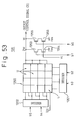
- Figure 53 is a block circuit diagram showing one example of a D/A converter for performing a digital-to-analog conversion (D/A conversion) of the outputs of the up-down counter shown in Figure 52.
- D/A conversion digital-to-analog conversion
- the third embodiment uses the up-down counter 134 instead of the charge pump circuit 131 in the first embodiment. More specifically, the up-down counter 134 counts the up signal UP and down signal DN supplied from the phase comparator circuit 312, and supplies, for example, a 6-bit count signal b0-b5 to the D/A converter 135 shown in Figure 53.
- each current matrix cell U comprises an AND gate UA, an OR gate UO, and two nMOS transistors UT1 and UT2; many such cells U are arranged in a matrix array to form a current matrix block 1350, and count signals (b2, b3; b4, b5) are supplied to the current matrix cells U via decoders 1351 and 1352.
- the high-order count signals b0 and b1 are supplied to the gates of nMOS transistors (1353 and 1355) in two transistor-pairs (1353, 1354; 1355, 1356) each consisting of two nMOS transistors connected in series between the output terminal and the low-level voltage supply line (Vss).
- the control voltage Vc is applied to the gates of the other transistors (1354 and 1356) in the respective transistor pairs. This control voltage Vc is also applied to the gate of the transistor UT2 in each current matrix cell U.
- the third embodiment shown in Figures 52 to 54 has the advantages that the design of a loop filter is facilitated, and that even when the phase comparison operation of the loop using the DLL circuit is completely stopped, the delay amount can be maintained at a constant level and power consumption can thus be reduced.
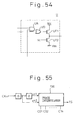
- Figure 55 is a block diagram showing the configuration of the timing signal generating circuit applicable to the slave circuit, as a fourth embodiment according to the third aspect of the present invention, and Figure 56 is a circuit diagram showing one example of a phase interpolator 136 in Figure 55.
- an input clock (in2) and a signal (in1) delayed by one stage relative to the input clock are supplied to the phase interpolator 136 which then generates the timing signal TS in the slave circuit 302.
- the phase interpolator 136 takes a weighted sum of the two inputs (in1 and in2) by varying the bias currents of input transistors (tail current) of a pair of differential amplifier stages 1361 and 1362, and supplies signals S1 and S2 from the two differential amplifier stages 1361 and 1362 to a comparator 1363 to obtain an output (timing signal TS) having an intermediate phase between the phases of the two signals S1 and S2.
- Weighting of the inputs in1 and in2 in the differential amplifier stages 1361 and 1362 can be accomplished, for example, by applying a control code (C01, C02, ..., C0n; C11, C12, ..., C1n) to one transistor (1364) in each transistor pair consisting of two nMOS transistors connected in series and a control voltage (Vcs) to the gate of the other transistor (1365) in each pair.
- a control code C01, C02, ..., C0n; C11, C12, ..., C1n
- Vcs control voltage
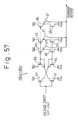
- Figure 57 is a circuit diagram showing another example of the phase interpolator 136 as a fifth embodiment according to the third aspect of the present invention.
- the phase interpolator 136 shown in Figure 57 comprises two voltage-to-current conversion circuits 136a and 136b each of which includes pMOS transistors 61 and 63 and nMOS transistors 62 and 64.
- the voltage-to-current conversion circuits 136a and 136b convert the voltage inputs in1 and in2 into current outputs.
- the number of output transistors (65 and 66) in each voltage-to-current conversion circuit is controlled by switch means 67 using an external signal, thus varying the conversion factor of the voltage-to-current conversion.
- the converted currents are summed, and the results are supplied to the comparator to obtain the timing signal (TS).
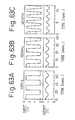
- Figure 58 is a circuit diagram showing the configuration of the timing signal generating circuit (phase interpolator 136) used to perform a simulation of the fifth embodiment according to the third aspect of the present invention
- Figure 59 is a diagram showing simulation results (SPICE simulation results) for the timing signal generating circuit of Figure 58.
- the phase interpolator 136 comprises the voltage-to-current conversion circuits 136a and 136b which respectively convert the input signals (voltage signals) in1 and in2 into current signals.
- a delay unit D (the same delay unit as used in the variable delay line 311: See Figure 45 or 49) is inserted at the input of each of the voltage-to-current conversion circuits 136a and 136b, and signals in1* and in2*, obtained by moderating the change of the input signals in1 and in2 through the respective delay units D, are supplied to the voltage-to-current conversion circuits 136a and 136b, respectively.
- Reference characters W 0 to W 7 (/W 0 to /W 7 ) in Figure 58 are the external signals used to control the switching of the transfer gates (switch means) 67; using these external signals W 0 to W 7 (/W 0 to /W 7 ), the transfer gates are opened or closed to control the number of output transistors (65 and 66) in the voltage-to-current conversion circuit 136a (136b). In this way, the timing of the output (Out) can be changed as shown in Figure 59. More specifically, by varying the conversion factor of the voltage-to-current conversion circuits 136a and 136b, the weights to be assigned to the two input signals in1 and in2 are varied, thereby implementing the operation of the phase interpolator 136.
- the phase interpolator of the fifth embodiment has the advantage of allowing further lower voltage operation because it does not use current-mirror deferential amplifier stages as in the fourth embodiment shown in Fig. 56.
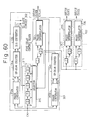
- Figure 60 is a block diagram showing the configuration of the timing signal generating circuit as a sixth embodiment according to the third aspect of the present invention.
- a DLL circuit is formed using the master circuit 301 and slave circuit 302; more specifically, a coarse delay control block for performing coarse delay control and a fine delay control block for performing fine delay control are provided in the master circuit 301, and a circuit corresponding to the fine delay control block in the master circuit 301 is included in the slave circuit 302.
- the coarse delay control block in the master circuit 301 comprises a delay line 311, a phase comparator circuit 312a, an up-down counter 134a, a D/A converter 135, and a selector 315
- the fine delay control block in the master circuit 301 comprises a phase interpolator 136 and two delay units D for delaying the output of the coarse delay control block (the selector 315), for example, by one and two delay stages and for supplying the delayed outputs to the phase interpolator 136.
- the reference clock CKr and the output of the final delay stage in the delay line 311 consisting, for example, of m delay units D are supplied as inputs to the phase comparator circuit 312a; further, an output (current control signal) from the D/A converter 135 is supplied to the delay line 311, which outputs to the selector 315 a timing signal whose phase is equally divided according to the number of stages of the delay units D.
- the selector 315 and the phase interpolator 136 are also supplied with a control signal generated by a phase comparator circuit 312b and up-down counter 134b. That is, the coarse delay control block takes taps off the delay line 311 consisting of the plurality of delay units, selects the output of each tap using the selector (selecting means) 315, and supplies the output signal to each fine delay control block.
- a delay with a resolution higher than the resolution of the delay line 311 can be produced using a digital signal, and a highly accurate DLL signal can thus be obtained.
- a digitally controlled DLL circuit can be achieved that allows the phase comparison operation to be stopped for a long period and that can resume operation in a short period from sleep mode.
- a plurality of fine delay control blocks phase interpolators 236) as slave circuits 302
- a plurality of timing signals each having a delay with a resolution higher than the resolution of the delay line 311, can be obtained.
- Figure 61 is a block diagram showing the configuration of the timing signal generating circuit as a seventh embodiment according to the third aspect of the present invention.
- the control signal CS (the output of the control signal generating circuit 313) but also three-phase internal clocks CK1 to CK3 (the delayed outputs of the delay line 311) are supplied from the master circuit 301 to the slave circuit 302.
- a timing signal (output clock) with a desired phase is generated by the phase interpolator 236, based on the three-phase clocks CK1 to CK3 supplied from the master circuit 301.
- the three-phase clocks CK1 to CK3 are supplied to a switch block 238 in the slave circuit 302 via delay units D provided, for example, to moderate the signal changes. Prescribed combinations of the three-phase clocks are selected by the switch block 238 and supplied to the inputs of operational amplifiers 237a and 237b. The outputs of the operational amplifiers 237a and 237b are supplied to the phase interpolator 236 where the phase is divided and a prescribed timing signal is produced for output.
- the seventh embodiment has the advantage that a timing signal (output clock) having a desired phase angle within 360 degrees can be generated in the slave circuit 302.
- FIG. 62 shows one example of the sinusoidal clock generating circuit applicable, for example, for use in the slave circuit 302.
- the delay unit D which operates with the control signal (CS) from the master circuit 301, is used for the portion that produces the triangular wave; since the delay in this delay unit D is proportional to the cycle of the reference clock (CKr), the amplitude of the triangular wave is maintained at a constant level regardless of variations in the reference clock frequency. Accordingly, the eighth embodiment has the advantage of being able to generate the sine wave over a wide frequency range.
- the sine wave generating circuit of Figure 62 can convert an input square wave to a substantially sinusoidal waveform.
- Figure 64 is a block diagram showing the configuration of the timing signal generating circuit as a ninth embodiment according to the third aspect of the present invention, dealing with an example of the timing signal generating circuit using a PLL circuit.
- reference numeral 312 is a phase comparator circuit
- 134 is an up-down counter
- 135 is a D/A converter
- 321 is a voltage-controlled oscillator (VCO).
- the voltage-controlled oscillator 321 is constructed from a ring oscillator formed, for example, by cascading three stages of circuits each similar in configuration to the delay unit D shown in Figure 49, and the control voltages Vcp and Vcn, output from the control signal generating circuit (current-to-voltage conversion circuit 133), are applied to the gates of the control transistors (DTp and DTn) in each stage to control the oscillation frequency.
- each slave circuit 302 comprises the current-to-voltage conversion circuit 133 and the voltage-controlled oscillator 321.
- the master circuit 301 uses the PLL circuit, not the DLL circuit, the output signal (timing signal) can be generated even in cases where a completely periodic clock signal cannot be obtained. That is, even when jitter is contained in the input reference clock CKr, for example, since the jitter component can be removed by the voltage-controlled oscillator (ring oscillator) 321, etc., the ninth embodiment is particularly preferable when recovering a clock component from the received data.
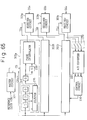
- Figure 65 is a block diagram showing the configuration of the timing signal generating circuit as a 10th embodiment according to the third aspect of the present invention.
- the master circuit 301 uses a DLL circuit that outputs an internal clock (CKin) locked on the reference clock (CKr), and slave circuits 302a to 302z are provided for the respective bits of multi-bit receiver circuits 303a to 303z.
- CKin internal clock
- CKr reference clock
- slave circuits 302a to 302z are provided for the respective bits of multi-bit receiver circuits 303a to 303z.
- the master circuit 301 is not limited to the one shown in Figure 60, but various other configurations are possible.
- the slave circuits 302a to 302z (302a) each comprise a selector 211, a delay line 215, two delay units D, and a phase interpolator 236, corresponding respectively to the selector (315), delay line (311), delay units (D), and phase interpolator (136) shown in Figure 60, and supply timing signals TSa to TSz to the corresponding receiver circuits 303a to 303z to control the timing for the respective receiver circuits 303a to 303z to latch signals SSa to SSz.
- the slave circuits 302a to 302z sequentially detect the levels of the signals SSa to SSz in the corresponding receiver circuits 303a to 303z, and control the respective delay amounts to provide optimum latch timing. More specifically, the signals from the receiver circuits are sequentially selected by a switch means 210 (for example, the signal SSa from the receiver circuit 303a is selected) and the selected signal is supplied to an A/D converter 220 for analog-to-digital conversion (A/D conversion); then, the selection (the delay amount in the delay line 211) by the selector 215 is controlled via a control circuit 230 so as to maximize the signal level (to increase the S/N ratio).
- the timing of the timing signal TSa is determined utilizing this characteristic.
- the delay amount in the delay line 211 is controlled using, for example, a 6-bit digital signal, and this digital signal is controlled so that the signal strength becomes the greatest in each of the receiver circuits 303a to 303z.
- a special signal for that purpose for example, a bit sequence "1010"
- the advantage is that, even for parallel signal transmission of multiple bits, the operation timing of each receiver circuit can be optimized by also considering the signal line delay between each bit.
- Figure 66 is a block diagram showing the configuration of an essential portion of the timing signal generating circuit as an 11th embodiment according to the third aspect of the present invention.
- each slave circuit 302 is provided with a fine delay control block using a phase interpolator 236, and controls input sampling timing (CL1, CL2) by using a 6-bit digital signal.
- reference numeral 212 is a combinational logic circuit
- 234 is an up-down counter
- 241 and 242 are receiving latch circuits.
- the phase interpolator 236 is supplied with outputs ( ⁇ 1, / ⁇ 1, ⁇ 2, / ⁇ 2) of a four-phase PLL circuit (250) in the master circuit 301, and outputs the control clocks CL1 and CL2 to control the sampling timing at the latch circuits 241 and 242.
- the latch circuits 241 and 242 are each constructed from two D-type flip-flops (D-FFs); sampling by the two flip-flops in the latch circuit 241 is controlled by the control clock CL1, while sampling by the two flip-flops in the latch circuit 242 is controlled by the control clocks CL1 and CL2, respectively.
- each slave circuit 302 (302a to 302z) of the 11th embodiment two receiving latch circuits.241 and 242 are provided for one bit; the latch circuit 241 samples the input at the center of a data receiving window (also called a bit cell), while the other latch circuit 242 samples at the boundary between two adjacent bit cells.
- the two latch circuits 241 and 242 are controlled by the control clocks CL1 and CL2 180 degrees out of phase with respect to each other, so that the input signal is sampled at a sampling rate twice the usual sampling rate.
- a decision signal (up signal UP or down signal DN) can be obtained that indicates whether the control clocks CL1 and CL2 should be delayed or advanced.
- This decision signal (UP, DN) is counted by the up-down counter 234, and the contents are converted to a 6-bit signal (C00, C01, C02; C10, C11, C12) which is supplied to the phase interpolator 236 to control the timing of the control clocks CL1 and CL2, thereby optimizing the signal receiving timing for maximum S/N ratio.
- the processing for the receiving timing optimization for each bit can be performed in parallel with data transmission and reception.
- the 6-bit signal (C00, C01, C02; C10, C11, C12) from the up-down counter 234 and the outputs ( ⁇ 1, / ⁇ 1, ⁇ 2, / ⁇ 2) from the four-phase PLL circuit (250) in the master circuit 301 are supplied to the phase interpolator 236.
- the differential inputs to differential amplifier stages 2361 and 2362 are weighted using the 6-bit signal.
- the outputs ( ⁇ 1, / ⁇ 1, ⁇ 2, / ⁇ 2) from the four-phase PLL circuit are supplied to the inputs of the respective differential amplifier stages 2361 and 2362 by being switched via a switch means 2360 which is controlled by control signals Sns and /Sns.
- the signals output from the pair of differential amplifier stages 2361 and 2362 are passed through an output stage (comparator) 2363 to produce the control clocks CL1 and CL2, as in the case of Figure 56 previously explained.
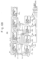
- the four-phase PLL circuit 250 comprises four stages of differential amplifier blocks 2511 to 2514, four signal conversion blocks 2521 to 2524, and four inverters 2531 to 2534. That is, the four differential amplifier blocks 2511 to 2514 are connected in cascade, prescribed signals are supplied to the signal conversion blocks 2521 and 2524, and signal levels are inverted and waveshaping performed by the inverters 2351 and 2354 to obtain the four-phase output signals ⁇ 1, / ⁇ 1, ⁇ 2, and / ⁇ 2.
- Figure 69 is a circuit diagram showing one example of the signal conversion block 252 (2521 to 2524) in the four-phase PLL circuit of Figure 68
- Figure 70 is a circuit diagram showing one example of the differential amplifier block 251 (2511 to 2514) in the four-phase PLL circuit of Figure 68.
- each signal conversion block 252 always outputs a signal (Z) of high level “H” when signal INH is at a high level "H", and a signal (Z), whose level is dependent on the input signals A and B, when the signal INH is at a low level “L” and control signal CTL is at a high level "H".
- the differential amplifier blocks 251 are cascaded so that the output signals (OUT1 and OUT2) from the differential amplifier blocks 2511, 2512, and 2513 are supplied as input signals IN1 and IN2 to the differential amplifier blocks 2512, 2513, and 2514 at the respective subsequent stages.
- the first-stage differential amplifier block 2511 are supplied the output signals from the last stage (fourth-stage) differential amplifier block 2514.
- Each differential amplifier block 251 is activated when the control signal CTL is at a high level "H".
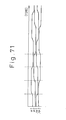
- Figure 71 is a diagram showing the output signals of the four-phase PLL circuit of Figure 68.
- the four-phase output signals ⁇ 1, ⁇ 2, / ⁇ 1, and /( ⁇ 2, one shifted in phase by 90 degrees with respect to the next, as shown in Figure 71, are obtained from the four-phase PLL circuit 250 constructed using the signal conversion blocks 252 and differential amplifier blocks 251 shown in Figures 69 and 70. As previously noted, these signals ⁇ 1, ⁇ 2, / ⁇ 1, and / ⁇ 2 are supplied to the phase interpolator 236 in the slave circuit 302 shown, for example, in Figure 66.
- the four-phase PLL circuit 250, the signal conversion blocks 252, and the differential amplifier blocks 251 are not limited in configuration to those described above, but various other circuit configurations are also possible.
- the timing signal synchronized to the reference clock can be generated in each slave circuit that is much simpler in configuration than the master circuit. Furthermore, by varying the response speed of the slave circuit according to the frequency of the reference clock, it becomes possible to generate a highly accurate timing signal over a wide frequency range. That is, timing pulses having a predetermined phase difference relative to each other can be generated synchronously with the reference clock by using many slave circuits that are simple in configuration, and highly accurate timing signals necessary for the transmission and reception of high-speed signals can be generated using circuitry that occupies a small area.
- the master circuit and the plurality of slave circuits can be provided within one semiconductor integrated circuit device (LSI chip), it is also possible to construct the master circuit and the slave circuits respectively on different semiconductor integrated circuit devices. That is, the timing signal generating circuit according to each embodiment in the third aspect of the present invention can also be applied to a semiconductor integrated circuit system having a plurality of semiconductor integrated circuit devices or to a multichip module (MCM) or the like.
- MCM multichip module
- a plurality of timing signals synchronized to the reference clock and having a predetermined phase difference relative to each other can be generated with high accuracy, using simple circuitry.
- the weighting control block 4301 is constructed from a plurality (the number n) of transfer gates provided in parallel between the input and output. These n (for example, 16) transfer gates are controlled for connection by control signals C41 to C4n, respectively, so that the sine wave f1 (f2) is weighted according to the number of transfer gates caused to conduct between the input and output. More specifically, in the circuit example of Figure 75, of the control signals C41 to C4n an arbitrary number of control signals are set to the high level "H", causing the corresponding number of transfer gates to turn on and thus varying the conductance (the conductance at the input side of the operational amplifier circuit 440).
- the analog summed waveform (the waveform at the other end of the capacitive load 4405) obtained by summing the positive logic digital periodic signals DIS1 and DIS2 (V1+ and V2+) is compared in the comparator 4407 with the analog summed waveform (the waveform at that other end of the capacitive load 4406) obtained by summing the negative logic digital periodic signals /DIS1 and ⁇ /DIS2 (V1- and V2-), and the digital periodic signal DO corresponding to the result of the comparison is output.
- weighting control for the digital periodic signals DIS1, DIS2, /DIS1, and /DIS2 is performed by changing the voltage level of the bias signals Vcp1, Vcn1, Vcp2, and Vcn2.
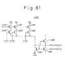
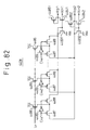
- Examples of the bias signal generating circuit (4408) for generating the bias signals are provided in Figures 81 and 82.
- bias signal generating circuits For the phase interpolator of Figure 80, two such bias signal generating circuits are needed, one for generating the bias signals Vcp1 and Vcn1 and the other for generating the bias signals Vcp2 and Vcn2, and the weighting control is performed such that when the positive logic control signals C431 to C43n are supplied to the bias signal generating circuit that generates the bias signals Vcp1 and Vcn1, for example, the complements of the control signals, /C431 to /C43n, are supplied to the bias signal generating circuit that generates the bias signals Vcp2 and Vcn2.
- the bias signal generating circuit 4408 shown in Figure 81 is constructed as a current-output type D/A converter, and the current source at the controlled side obtains a variable constant current by mirroring the current received from the D/A converter by using the current mirror circuit, and generates the bias signals Vcp1 (Vcp2) and Vcn1 (Vcn2) having a prescribed voltage level appropriate to the control signals C431 to C43n. Since the current source at the controlled side can be simplified in configuration, the advantage is that the bias signal generating circuit is realizable with a small amount of circuitry.
- the drain of each of a plurality of pMOS transistors 4486, each supplied with the reference voltage (Vr), is connected to one end (the source) of each of pMOS transistors 4487 and 4488 whose switching operations are controlled by control signals (digital signals) C441 to C44n.
- the transistors 4487 in the respective transistor pairs are supplied at their gates with the corresponding control signals C441 to C44n, while the transistors 4488 in the respective transistor pairs are supplied at their gates with the control signals (/C441 to /C44n) inverted by respective inverters 4489. Accordingly, in each transistor pair one of the transistors, 4487 or 4488, is ON and the other is OFF.
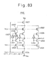
- Figure 83 is a circuit diagram showing the configuration of a variable current source (4500) as a modified example of the 16th embodiment of Figure 80. This example is applicable to each constant current source (4401 to 4404) in the previously described phase interpolator of Figure 80.
- the bias signals (bias voltages) Vcp and Vcn are constant-voltage-level signals, and weighting control is performed using control signals C451 to C45n.
- the node between the transistors 4506 and 4508 in each pair is connected in common with the corresponding nodes in the other pairs, to produce an output (output terminal) "out".
- the output terminal "out” is connected, for example, to one end of the capacitive load (4405 or 4406) and one input terminal of the comparator (4407), as shown in Figure 80.
- variable current source of the modified example shown in Figure 83 controls the number of output transistors (4506 and 4508) in the current mirror to obtain the variable current source, and maintains the gate bias (bias signals Vcp and Vcn) of the current-mirror operating transistors (4502 and 4503) always at a constant level. This serves to enhance the current stability. Further, the variable current source of the modified example has the advantage of excellent linearity because current control is accomplished by controlling the number of transistors.
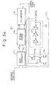
- Figure 84 is a circuit diagram showing a configurational example of a portion of the phase interpolator as a 17th embodiment of the present invention, in which a clamp circuit 4600 is provided between the two input terminals of the comparator 4407 in the phase interpolator of Figure 80.
- the clamp circuit 4600 When the clamp circuit 4600 is provided, for example, between the two input terminals (the nodes where analog waveforms are generated by summing) of the comparator 4407 in the phase interpolator of Figure 80, as shown in Figure 84, the common mode potentials of these nodes are maintained constant by the clamp circuit 4600 even if there occurs an unbalance in the current values of the current sources. As a result, the comparator 4407 at the subsequent stage can always perform the compare operation under a constant condition, and timing accuracy can thus be enhanced.
- the clamp circuit 4600 shown in Figure 84 is configured so that 1/2•Vcc (reference voltage) is applied to the gates of two nMOS transistors 4601 and 4602 connected in series and also to the node between these transistors 4601 and 4602, to clamp the voltage between the two input terminals of the comparator 4407.
- 1/2•Vcc reference voltage
- various configurations other than that shown in Figure 84 are applicable.
- Figure 85 is a diagram for explaining a configurational example of the phase interpolator as an 18th embodiment of the present invention.
- the horizontal axis represents D/A input code, that is, the number of transistors selected (connected) by control signals, and the vertical axis shows the output current as the sum of the currents flowing through the selected transistors.
- the phase interpolator of the present invention selects a plurality of transistors, for example, of the same size by using control signals (digital signals), thereby controlling the number of transistors to be connected and thus adjusting the current output.
- the number of transistors 4482 to be caused to conduct (connected) is controlled in accordance with the control signals C431 to C43n, and the sum of the currents flowing through the conducting transistors 4482 flows to the transistor 4483.
- the size of each transistor 4482 (4481) is adjusted so that a linear relationship is maintained between the current (output current) flowing to the transistor 4483 and the number of transistors 4482 conducting in accordance with the control signals C431 to C43n.
- This transistor size adjustment can be applied not only to the transistors in the above-described current D/A converter but also to the transistors (for example, the transistors 4483, 4484, 4485, etc.) associated with the current mirror circuit, etc. in order to compensate for nonlinear components occurring in the current mirror circuit, etc.
Landscapes
- Engineering & Computer Science (AREA)
- Microelectronics & Electronic Packaging (AREA)
- Computer Networks & Wireless Communication (AREA)
- Signal Processing (AREA)
- Computer Hardware Design (AREA)
- Dram (AREA)
- Pulse Circuits (AREA)
Applications Claiming Priority (9)
| Application Number | Priority Date | Filing Date | Title |
|---|---|---|---|
| JP15542997 | 1997-06-12 | ||
| JP15542997A JP3961072B2 (ja) | 1997-06-12 | 1997-06-12 | 半導体装置及びそのタイミング調整方法 |
| JP225498 | 1998-01-08 | ||
| JP225498 | 1998-01-08 | ||
| JP7940198 | 1998-03-26 | ||
| JP07940198A JP4063392B2 (ja) | 1998-03-26 | 1998-03-26 | 信号伝送システム |
| JP13561098A JP3955150B2 (ja) | 1998-01-08 | 1998-05-18 | 位相インターポレータ、タイミング信号発生回路、および、該タイミング信号発生回路が適用される半導体集積回路装置並びに半導体集積回路システム |
| JP13561098 | 1998-05-18 | ||
| EP98110643A EP0884732B1 (fr) | 1997-06-12 | 1998-06-10 | Circuit de temporisation, dispositif et système intégré à semiconducteurs auxquels le circuit de temporisation est connecté, et système de transmission de signaux |
Related Parent Applications (2)
| Application Number | Title | Priority Date | Filing Date |
|---|---|---|---|
| EP98110643A Division EP0884732B1 (fr) | 1997-06-12 | 1998-06-10 | Circuit de temporisation, dispositif et système intégré à semiconducteurs auxquels le circuit de temporisation est connecté, et système de transmission de signaux |
| EP98110643.8 Division | 1998-06-10 |
Publications (3)
| Publication Number | Publication Date |
|---|---|
| EP1492120A2 true EP1492120A2 (fr) | 2004-12-29 |
| EP1492120A3 EP1492120A3 (fr) | 2005-02-02 |
| EP1492120B1 EP1492120B1 (fr) | 2007-04-25 |
Family
ID=27453587
Family Applications (4)
| Application Number | Title | Priority Date | Filing Date |
|---|---|---|---|
| EP04014102A Expired - Lifetime EP1492120B1 (fr) | 1997-06-12 | 1998-06-10 | Circuit de temporisation, dispositif et système intégré à semiconducteurs auxquels le circuit de temporisation est connecté, et système de transmission de signaux |
| EP04014103A Expired - Lifetime EP1492121B1 (fr) | 1997-06-12 | 1998-06-10 | Circuit de temporisation, dispositif et système intégré à semiconducteurs auxquels le circuit de temporisation est connecté, et système de transmission de signaux |
| EP04014101A Expired - Lifetime EP1489619B1 (fr) | 1997-06-12 | 1998-06-10 | Circuit de temporisation, dispositif et système intégré à semiconducteurs auxquels le circuit de temporisation est connecté, et système de transmission de signaux |
| EP98110643A Expired - Lifetime EP0884732B1 (fr) | 1997-06-12 | 1998-06-10 | Circuit de temporisation, dispositif et système intégré à semiconducteurs auxquels le circuit de temporisation est connecté, et système de transmission de signaux |
Family Applications After (3)
| Application Number | Title | Priority Date | Filing Date |
|---|---|---|---|
| EP04014103A Expired - Lifetime EP1492121B1 (fr) | 1997-06-12 | 1998-06-10 | Circuit de temporisation, dispositif et système intégré à semiconducteurs auxquels le circuit de temporisation est connecté, et système de transmission de signaux |
| EP04014101A Expired - Lifetime EP1489619B1 (fr) | 1997-06-12 | 1998-06-10 | Circuit de temporisation, dispositif et système intégré à semiconducteurs auxquels le circuit de temporisation est connecté, et système de transmission de signaux |
| EP98110643A Expired - Lifetime EP0884732B1 (fr) | 1997-06-12 | 1998-06-10 | Circuit de temporisation, dispositif et système intégré à semiconducteurs auxquels le circuit de temporisation est connecté, et système de transmission de signaux |
Country Status (5)
| Country | Link |
|---|---|
| US (4) | US6247138B1 (fr) |
| EP (4) | EP1492120B1 (fr) |
| KR (4) | KR100313820B1 (fr) |
| DE (4) | DE69833467T2 (fr) |
| TW (1) | TW387065B (fr) |
Families Citing this family (273)
| Publication number | Priority date | Publication date | Assignee | Title |
|---|---|---|---|---|
| US5978379A (en) | 1997-01-23 | 1999-11-02 | Gadzoox Networks, Inc. | Fiber channel learning bridge, learning half bridge, and protocol |
| JP4197755B2 (ja) | 1997-11-19 | 2008-12-17 | 富士通株式会社 | 信号伝送システム、該信号伝送システムのレシーバ回路、および、該信号伝送システムが適用される半導体記憶装置 |
| DE69939291D1 (de) | 1998-04-28 | 2008-09-25 | Matsushita Electric Industrial Co Ltd | Eingangsschaltung |
| TW440767B (en) * | 1998-06-02 | 2001-06-16 | Fujitsu Ltd | Method of and apparatus for correctly transmitting signals at high speed without waveform distortion |
| US7430171B2 (en) | 1998-11-19 | 2008-09-30 | Broadcom Corporation | Fibre channel arbitrated loop bufferless switch circuitry to increase bandwidth without significant increase in cost |
| US6285216B1 (en) * | 1998-12-17 | 2001-09-04 | United Microelectronics Corporation | High speed output enable path and method for an integrated circuit device |
| US6636993B1 (en) * | 1999-02-12 | 2003-10-21 | Fujitsu Limited | System and method for automatic deskew across a high speed, parallel interconnection |
| JP3789247B2 (ja) * | 1999-02-26 | 2006-06-21 | Necエレクトロニクス株式会社 | クロック周期検知回路 |
| US6111796A (en) * | 1999-03-01 | 2000-08-29 | Motorola, Inc. | Programmable delay control for sense amplifiers in a memory |
| US6654897B1 (en) * | 1999-03-05 | 2003-11-25 | International Business Machines Corporation | Dynamic wave-pipelined interface apparatus and methods therefor |
| US6928128B1 (en) * | 1999-05-03 | 2005-08-09 | Rambus Inc. | Clock alignment circuit having a self regulating voltage supply |
| US6424194B1 (en) | 1999-06-28 | 2002-07-23 | Broadcom Corporation | Current-controlled CMOS logic family |
| JP2001156255A (ja) * | 1999-11-25 | 2001-06-08 | Oki Electric Ind Co Ltd | 半導体集積回路 |
| TW483255B (en) * | 1999-11-26 | 2002-04-11 | Fujitsu Ltd | Phase-combining circuit and timing signal generator circuit for carrying out a high-speed signal transmission |
| US6961363B1 (en) * | 1999-12-02 | 2005-11-01 | International Business Machines Corporation | Frequency look-ahead and link state history based scheduling in indoor wireless pico-cellular networks |
| US7315599B1 (en) * | 1999-12-29 | 2008-01-01 | Intel Corporation | Skew correction circuit |
| IT1311463B1 (it) * | 1999-12-31 | 2002-03-12 | Cit Alcatel | Metodo di recupero del segnale d'orologio in un sistema ditelecomunicazioni e relativo circuito. |
| JP4301680B2 (ja) * | 2000-02-29 | 2009-07-22 | 株式会社ルネサステクノロジ | 半導体集積回路装置 |
| JP3495311B2 (ja) * | 2000-03-24 | 2004-02-09 | Necエレクトロニクス株式会社 | クロック制御回路 |
| WO2001084702A2 (fr) | 2000-04-28 | 2001-11-08 | Broadcom Corporation | Systemes emetteurs-recepteurs tres rapides de donnees serie et procedes apparentes |
| US6658580B1 (en) * | 2000-05-20 | 2003-12-02 | Equipe Communications Corporation | Redundant, synchronous central timing systems with constant master voltage controls and variable slave voltage controls |
| JP3667196B2 (ja) | 2000-05-26 | 2005-07-06 | Necエレクトロニクス株式会社 | タイミング差分割回路 |
| US7006635B2 (en) * | 2000-08-31 | 2006-02-28 | The United States Of America As Represented By The Secretary Of The Navy | Method and apparatus for clock synchronization using quantum mechanical non-locality effects |
| US6889272B1 (en) * | 2000-11-03 | 2005-05-03 | Applied Micro Circuits Corporation | Parallel data bus with bit position encoded on the clock wire |
| US7405732B2 (en) * | 2000-12-07 | 2008-07-29 | Renesas Technology Corp. | Semiconductor integrated circuit, liquid crystal drive device, and liquid crystal display system |
| JP4592179B2 (ja) | 2000-12-19 | 2010-12-01 | ルネサスエレクトロニクス株式会社 | ディレイロックドループ、当該ディレイロックドループを含む半導体装置およびクロック同期により動作するシステムのための制御方法 |
| DE10064929A1 (de) * | 2000-12-23 | 2002-07-04 | Alcatel Sa | Verfahren und Kompensationsmodul zur Phasenkompensation von Taktsignalen |
| US6304119B1 (en) * | 2000-12-27 | 2001-10-16 | Chroma Ate Inc. | Timing generating apparatus with self-calibrating capability |
| US7050512B1 (en) * | 2001-01-08 | 2006-05-23 | Pixelworks, Inc. | Receiver architecture |
| JP3558599B2 (ja) * | 2001-02-02 | 2004-08-25 | 日本電気株式会社 | データ伝送システム及びデータ伝送方法 |
| US6675272B2 (en) | 2001-04-24 | 2004-01-06 | Rambus Inc. | Method and apparatus for coordinating memory operations among diversely-located memory components |
| US8391039B2 (en) | 2001-04-24 | 2013-03-05 | Rambus Inc. | Memory module with termination component |
| JP3918145B2 (ja) * | 2001-05-21 | 2007-05-23 | 株式会社ルネサステクノロジ | メモリコントローラ |
| WO2002095943A2 (fr) * | 2001-05-21 | 2002-11-28 | Vasily Grigorievich Atyunin | Vernier programmable a etalonnage automatique et procede |
| US7194059B2 (en) * | 2001-08-17 | 2007-03-20 | Zarlink Semiconductor, Inc. | Method and apparatus for skip-free retiming transmission of digital information |
| US7243323B2 (en) * | 2001-08-29 | 2007-07-10 | Infineon Technologies Ag | Integrated circuit chip design |
| US6504438B1 (en) * | 2001-09-17 | 2003-01-07 | Rambus, Inc. | Dual loop phase lock loops using dual voltage supply regulators |
| KR100487637B1 (ko) * | 2001-09-20 | 2005-05-03 | 주식회사 하이닉스반도체 | 디지털 지연 라인 |
| JP4308461B2 (ja) * | 2001-10-05 | 2009-08-05 | ラムバス・インコーポレーテッド | 半導体記憶装置 |
| US6930524B2 (en) * | 2001-10-09 | 2005-08-16 | Micron Technology, Inc. | Dual-phase delay-locked loop circuit and method |
| US6920540B2 (en) | 2001-10-22 | 2005-07-19 | Rambus Inc. | Timing calibration apparatus and method for a memory device signaling system |
| US6759911B2 (en) | 2001-11-19 | 2004-07-06 | Mcron Technology, Inc. | Delay-locked loop circuit and method using a ring oscillator and counter-based delay |
| US7203259B2 (en) * | 2002-01-02 | 2007-04-10 | Intel Corporation | Phase interpolator |
| US20030135675A1 (en) * | 2002-01-17 | 2003-07-17 | Koninklijke Philips Electronics N.V. | Configurable synchronous or asynchronous bus interface |
| US7103126B2 (en) * | 2002-01-17 | 2006-09-05 | Micron Technology, Inc. | Method and circuit for adjusting the timing of output data based on the current and future states of the output data |
| JP4107847B2 (ja) | 2002-02-01 | 2008-06-25 | 富士通株式会社 | タイミング信号発生回路および受信回路 |
| EP1476800B1 (fr) * | 2002-02-14 | 2010-11-17 | TELEFONAKTIEBOLAGET LM ERICSSON (publ) | Signaux d'horloge continus |
| GB2385728B (en) * | 2002-02-26 | 2006-07-12 | Fujitsu Ltd | Clock recovery circuitry |
| US7035368B2 (en) * | 2002-03-18 | 2006-04-25 | Texas Instruments Incorporated | High speed parallel link receiver |
| US6642760B1 (en) | 2002-03-29 | 2003-11-04 | Rambus, Inc. | Apparatus and method for a digital delay locked loop |
| US6621316B1 (en) | 2002-06-20 | 2003-09-16 | Micron Technology, Inc. | Synchronous mirror delay (SMD) circuit and method including a counter and reduced size bi-directional delay line |
| US7047384B2 (en) * | 2002-06-27 | 2006-05-16 | Intel Corporation | Method and apparatus for dynamic timing of memory interface signals |
| US7085993B2 (en) * | 2002-07-29 | 2006-08-01 | International Business Machine Corporation | System and method for correcting timing signals in integrated circuits |
| US6727740B2 (en) | 2002-08-29 | 2004-04-27 | Micron Technology, Inc. | Synchronous mirror delay (SMD) circuit and method including a ring oscillator for timing coarse and fine delay intervals |
| DE60209465D1 (de) * | 2002-09-02 | 2006-04-27 | St Microelectronics Srl | Hochgeschwindigkeitschnittstelle für Funkanlagen |
| US7123675B2 (en) * | 2002-09-25 | 2006-10-17 | Lucent Technologies Inc. | Clock, data and time recovery using bit-resolved timing registers |
| JP2004127147A (ja) * | 2002-10-07 | 2004-04-22 | Hitachi Ltd | デスキュー回路およびそれを用いたディスクアレイ制御装置 |
| WO2004046943A1 (fr) * | 2002-11-19 | 2004-06-03 | Fujitsu Limited | Circuit de traitement de signal |
| US7356720B1 (en) * | 2003-01-30 | 2008-04-08 | Juniper Networks, Inc. | Dynamic programmable delay selection circuit and method |
| US6937076B2 (en) * | 2003-06-11 | 2005-08-30 | Micron Technology, Inc. | Clock synchronizing apparatus and method using frequency dependent variable delay |
| KR100583951B1 (ko) * | 2003-07-11 | 2006-05-26 | 삼성전자주식회사 | 메모리 시스템 및 이 시스템의 타이밍 조절 방법 |
| DE10331829B4 (de) * | 2003-07-14 | 2009-04-16 | Qimonda Ag | Verfahren und Vorrichtung zur Erzeugung einer Referenzspannung |
| US6930932B2 (en) * | 2003-08-27 | 2005-08-16 | Hewlett-Packard Development Company, L.P. | Data signal reception latch control using clock aligned relative to strobe signal |
| JP4100300B2 (ja) * | 2003-09-02 | 2008-06-11 | セイコーエプソン株式会社 | 信号出力調整回路及び表示ドライバ |
| JP4632652B2 (ja) * | 2003-10-10 | 2011-02-16 | 日本電気株式会社 | 量子暗号鍵配布システム及びそれに用いる同期方法 |
| KR100512940B1 (ko) * | 2003-10-27 | 2005-09-07 | 삼성전자주식회사 | 데이터 전송 시스템 및 방법 |
| JP4237038B2 (ja) * | 2003-12-01 | 2009-03-11 | エルピーダメモリ株式会社 | 半導体集積回路装置 |
| US6958634B2 (en) * | 2003-12-24 | 2005-10-25 | Intel Corporation | Programmable direct interpolating delay locked loop |
| US7310751B2 (en) * | 2004-02-20 | 2007-12-18 | Hewlett-Packard Development Company, L.P. | Timeout event trigger generation |
| JP2005244479A (ja) * | 2004-02-25 | 2005-09-08 | Fujitsu Ltd | 伝送装置 |
| JP3982517B2 (ja) * | 2004-05-12 | 2007-09-26 | 日本電気株式会社 | データ伝送システム、制御装置及びその方法 |
| KR100608365B1 (ko) * | 2004-05-17 | 2006-08-08 | 주식회사 하이닉스반도체 | 메모리 장치의 내부 제어 신호를 측정하는 방법 및 장치 |
| GB0413071D0 (en) * | 2004-06-12 | 2004-07-14 | Texas Instruments Ltd | Triangulating phase interpolator |
| US7043392B2 (en) * | 2004-06-16 | 2006-05-09 | Intel Corporation | Interpolator testing system |
| JP4291225B2 (ja) * | 2004-06-30 | 2009-07-08 | 富士通株式会社 | パラレルデータを受信する装置および方法 |
| DE102004032547A1 (de) * | 2004-07-06 | 2006-02-02 | Atmel Germany Gmbh | Transponder mit einer Taktversorgungseinheit |
| US7149145B2 (en) | 2004-07-19 | 2006-12-12 | Micron Technology, Inc. | Delay stage-interweaved analog DLL/PLL |
| JP4419067B2 (ja) * | 2004-07-26 | 2010-02-24 | 株式会社日立製作所 | ディジタルインターフェースを有する半導体装置、メモリ素子及びメモリモジュール |
| US7301831B2 (en) | 2004-09-15 | 2007-11-27 | Rambus Inc. | Memory systems with variable delays for write data signals |
| EP1643644B1 (fr) * | 2004-09-30 | 2017-07-12 | Infineon Technologies AG | Un circuit à retard avec conversion précise temps-fréquence |
| US7173877B2 (en) * | 2004-09-30 | 2007-02-06 | Infineon Technologies Ag | Memory system with two clock lines and a memory device |
| US7130226B2 (en) * | 2005-02-09 | 2006-10-31 | Micron Technology, Inc. | Clock generating circuit with multiple modes of operation |
| US7412618B2 (en) * | 2005-02-11 | 2008-08-12 | International Business Machines Corporation | Combined alignment scrambler function for elastic interface |
| US7461287B2 (en) * | 2005-02-11 | 2008-12-02 | International Business Machines Corporation | Elastic interface de-skew mechanism |
| US7583772B2 (en) * | 2005-02-22 | 2009-09-01 | Broadcom Corporation | System for shifting data bits multiple times per clock cycle |
| JP2006260190A (ja) * | 2005-03-17 | 2006-09-28 | Fujitsu Ltd | マージンレス判定回路 |
| JP2006295668A (ja) * | 2005-04-13 | 2006-10-26 | Matsushita Electric Ind Co Ltd | 信号発生装置および方法ならびに半導体集積回路システム |
| EP1878116A4 (fr) * | 2005-04-18 | 2010-04-07 | Agency Science Tech & Res | Appareil de temporisation |
| US7602859B2 (en) * | 2005-04-28 | 2009-10-13 | Intel Corporation | Calibrating integrating receivers for source synchronous protocol |
| US20060245473A1 (en) * | 2005-04-28 | 2006-11-02 | Cheng Roger K | Integrating receivers for source synchronous protocol |
| KR100679261B1 (ko) * | 2005-05-10 | 2007-02-05 | 삼성전자주식회사 | 위상 인터폴레이션 회로 및 그에 따른 위상 인터폴레이션신호의 발생방법 |
| KR100615700B1 (ko) | 2005-08-23 | 2006-08-28 | 삼성전자주식회사 | 메모리 제어장치 및 그의 메모리 제어방법 |
| US7366966B2 (en) * | 2005-10-11 | 2008-04-29 | Micron Technology, Inc. | System and method for varying test signal durations and assert times for testing memory devices |
| KR100672033B1 (ko) * | 2005-10-14 | 2007-01-19 | 삼성전자주식회사 | 두 개의 입력 기준 클럭을 가지는 지연동기루프회로, 이를포함하는 클럭 신호 발생 회로 및 클럭 신호 발생 방법 |
| JP4955250B2 (ja) | 2005-10-14 | 2012-06-20 | ルネサスエレクトロニクス株式会社 | 半導体装置及びそのテスト方法 |
| JP4751178B2 (ja) * | 2005-10-27 | 2011-08-17 | エルピーダメモリ株式会社 | 同期型半導体装置 |
| US7379382B2 (en) * | 2005-10-28 | 2008-05-27 | Micron Technology, Inc. | System and method for controlling timing of output signals |
| US7614737B2 (en) * | 2005-12-16 | 2009-11-10 | Lexmark International Inc. | Method for identifying an installed cartridge |
| US7375558B2 (en) * | 2005-12-21 | 2008-05-20 | Integrated Device Technology, Inc. | Method and apparatus for pre-clocking |
| KR100759786B1 (ko) * | 2006-02-01 | 2007-09-20 | 삼성전자주식회사 | 반도체 장치의 지연동기루프 회로 및 지연동기루프제어방법 |
| FR2901930B1 (fr) * | 2006-05-31 | 2008-09-05 | Valeo Equip Electr Moteur | Procede et dispositif de generation de signaux binaires dephases et leur utilisation |
| KR100809690B1 (ko) * | 2006-07-14 | 2008-03-07 | 삼성전자주식회사 | 저속 테스트 동작이 가능한 반도체 메모리 장치 및 반도체메모리 장치의 테스트 방법 |
| US7908528B1 (en) * | 2006-10-09 | 2011-03-15 | Altera Corporation | Phase-detector-less method and apparatus for minimizing skew between bonded channel groups |
| US20080084955A1 (en) * | 2006-10-10 | 2008-04-10 | Wei-Zen Chen | Fast-locked clock and data recovery circuit and the method thereof |
| US7593273B2 (en) * | 2006-11-06 | 2009-09-22 | Altera Corporation | Read-leveling implementations for DDR3 applications on an FPGA |
| KR100801032B1 (ko) * | 2006-11-15 | 2008-02-04 | 삼성전자주식회사 | 비휘발성 반도체 메모리 장치의 입력회로 및 비휘발성반도체 메모리 장치의 데이터 입력방법 |
| JP4968671B2 (ja) * | 2006-11-27 | 2012-07-04 | Nltテクノロジー株式会社 | 半導体回路、走査回路、及びそれを用いた表示装置 |
| JP2008140821A (ja) * | 2006-11-30 | 2008-06-19 | Matsushita Electric Ind Co Ltd | 半導体装置および半導体装置の設計方法 |
| GB2444745B (en) * | 2006-12-13 | 2011-08-24 | Advanced Risc Mach Ltd | Data transfer between a master and slave |
| KR100855980B1 (ko) * | 2007-02-16 | 2008-09-02 | 삼성전자주식회사 | 쉬프터와 가산기를 이용하여 지연 시간을 조절하는 지연고정 루프 및 클럭 지연 방법 |
| JP4357538B2 (ja) * | 2007-03-07 | 2009-11-04 | 株式会社日立製作所 | 半導体集積回路装置 |
| US7429944B1 (en) * | 2007-03-20 | 2008-09-30 | Analog Devices, Inc. | Converter systems having reduced-jitter, selectively-skewed interleaved clocks |
| JP2008251070A (ja) * | 2007-03-29 | 2008-10-16 | Hitachi Ltd | 半導体記憶装置 |
| EP1976105B1 (fr) * | 2007-03-30 | 2011-09-21 | Alstom Technology Ltd | Séquence de contrôle de générateur actif |
| KR100892640B1 (ko) * | 2007-05-10 | 2009-04-09 | 주식회사 하이닉스반도체 | 반도체 집적 회로 |
| JP4657252B2 (ja) * | 2007-06-04 | 2011-03-23 | 三洋電機株式会社 | チャージポンプ回路及びスライスレベルコントロール回路 |
| US8615205B2 (en) * | 2007-12-18 | 2013-12-24 | Qualcomm Incorporated | I-Q mismatch calibration and method |
| GB0807625D0 (en) * | 2008-04-25 | 2008-06-04 | Glonav Ltd | Method and system for detecting timing characteristics in a communications system |
| US7728638B2 (en) * | 2008-04-25 | 2010-06-01 | Qimonda North America Corp. | Electronic system that adjusts DLL lock state acquisition time |
| US8970272B2 (en) * | 2008-05-15 | 2015-03-03 | Qualcomm Incorporated | High-speed low-power latches |
| US8521979B2 (en) | 2008-05-29 | 2013-08-27 | Micron Technology, Inc. | Memory systems and methods for controlling the timing of receiving read data |
| US7979757B2 (en) | 2008-06-03 | 2011-07-12 | Micron Technology, Inc. | Method and apparatus for testing high capacity/high bandwidth memory devices |
| US8041537B2 (en) * | 2008-06-27 | 2011-10-18 | International Business Machines Corporation | Clock duty cycle measurement with charge pump without using reference clock calibration |
| US8756486B2 (en) * | 2008-07-02 | 2014-06-17 | Micron Technology, Inc. | Method and apparatus for repairing high capacity/high bandwidth memory devices |
| US8289760B2 (en) | 2008-07-02 | 2012-10-16 | Micron Technology, Inc. | Multi-mode memory device and method having stacked memory dice, a logic die and a command processing circuit and operating in direct and indirect modes |
| US7855931B2 (en) | 2008-07-21 | 2010-12-21 | Micron Technology, Inc. | Memory system and method using stacked memory device dice, and system using the memory system |
| US7940202B1 (en) | 2008-07-31 | 2011-05-10 | Cypress Semiconductor Corporation | Clocking analog components operating in a digital system |
| US8127204B2 (en) * | 2008-08-15 | 2012-02-28 | Micron Technology, Inc. | Memory system and method using a memory device die stacked with a logic die using data encoding, and system using the memory system |
| US8510589B2 (en) * | 2008-08-29 | 2013-08-13 | Intel Mobile Communications GmbH | Apparatus and method using first and second clocks |
| KR20100037427A (ko) * | 2008-10-01 | 2010-04-09 | 삼성전자주식회사 | Ac 커플링 위상 보간기 및 이 장치를 이용하는 지연 고정루프 |
| JP5284756B2 (ja) * | 2008-10-31 | 2013-09-11 | 凸版印刷株式会社 | 電源回路及び電源安定化方法 |
| US8712357B2 (en) * | 2008-11-13 | 2014-04-29 | Qualcomm Incorporated | LO generation with deskewed input oscillator signal |
| US8718574B2 (en) | 2008-11-25 | 2014-05-06 | Qualcomm Incorporated | Duty cycle adjustment for a local oscillator signal |
| KR100992004B1 (ko) * | 2008-12-12 | 2010-11-04 | 주식회사 하이닉스반도체 | 반도체 메모리 장치의 도메인 크로싱 회로 |
| JP5353277B2 (ja) * | 2009-02-06 | 2013-11-27 | 日本電気株式会社 | ストリーム信号伝送装置及び伝送方法 |
| US8850256B2 (en) * | 2009-05-18 | 2014-09-30 | Nec Corporation | Communication circuit and communication method |
| US8063683B2 (en) * | 2009-06-08 | 2011-11-22 | Integrated Device Technology, Inc. | Low power clock and data recovery phase interpolator |
| US8386829B2 (en) * | 2009-06-17 | 2013-02-26 | Macronix International Co., Ltd. | Automatic internal trimming calibration method to compensate process variation |
| US8847638B2 (en) * | 2009-07-02 | 2014-09-30 | Qualcomm Incorporated | High speed divide-by-two circuit |
| US8791740B2 (en) | 2009-07-16 | 2014-07-29 | Qualcomm Incorporated | Systems and methods for reducing average current consumption in a local oscillator path |
| US7994837B1 (en) * | 2009-08-07 | 2011-08-09 | Altera Corporation | Techniques for phase interpolation |
| JP2011045220A (ja) * | 2009-08-24 | 2011-03-03 | Panasonic Corp | 端末装置及び供給電流制御方法 |
| US7944300B2 (en) * | 2009-08-25 | 2011-05-17 | Micron Technology, Inc. | Bias circuit and amplifier providing constant output current for a range of common mode inputs |
| US8289061B2 (en) * | 2009-09-29 | 2012-10-16 | Integrated Device Technology, Inc. | Technique to reduce clock recovery amplitude modulation in high-speed serial transceiver |
| JP4843704B2 (ja) * | 2009-09-30 | 2011-12-21 | 日本電波工業株式会社 | 周波数シンセサイザ |
| US8832336B2 (en) * | 2010-01-30 | 2014-09-09 | Mosys, Inc. | Reducing latency in serializer-deserializer links |
| JP2011160369A (ja) * | 2010-02-04 | 2011-08-18 | Sony Corp | 電子回路、電子機器、デジタル信号処理方法 |
| US8320149B2 (en) * | 2010-02-04 | 2012-11-27 | Richtek Technology Corporation, R.O.C. | Multi-chip module with master-slave analog signal transmission function |
| JP2011234157A (ja) * | 2010-04-28 | 2011-11-17 | Elpida Memory Inc | 半導体装置 |
| US9288089B2 (en) | 2010-04-30 | 2016-03-15 | Ecole Polytechnique Federale De Lausanne (Epfl) | Orthogonal differential vector signaling |
| US9288082B1 (en) | 2010-05-20 | 2016-03-15 | Kandou Labs, S.A. | Circuits for efficient detection of vector signaling codes for chip-to-chip communication using sums of differences |
| US9251873B1 (en) | 2010-05-20 | 2016-02-02 | Kandou Labs, S.A. | Methods and systems for pin-efficient memory controller interface using vector signaling codes for chip-to-chip communications |
| US9077386B1 (en) | 2010-05-20 | 2015-07-07 | Kandou Labs, S.A. | Methods and systems for selection of unions of vector signaling codes for power and pin efficient chip-to-chip communication |
| WO2011148467A1 (fr) * | 2010-05-25 | 2011-12-01 | 富士通株式会社 | Interpolateur de phase, circuiterie de réception et dispositif de traitement d'informations |
| WO2011156041A1 (fr) * | 2010-06-08 | 2011-12-15 | Rambus Inc. | Etalonnage de synchronisation d'un dispositif de circuit intégré |
| TWI425364B (zh) * | 2010-06-22 | 2014-02-01 | 晨星半導體股份有限公司 | 記憶體共享系統及方法 |
| DE102010034112A1 (de) | 2010-08-12 | 2012-02-16 | Gm Global Technology Operations Llc (N.D.Ges.D. Staates Delaware) | Interner Wärmetauscher für eine Kraftfahrzeug-Klimaanlage |
| KR101180405B1 (ko) * | 2010-09-03 | 2012-09-10 | 에스케이하이닉스 주식회사 | 반도체 메모리 장치 및 이의 테스트 방법 |
| US8400808B2 (en) | 2010-12-16 | 2013-03-19 | Micron Technology, Inc. | Phase interpolators and push-pull buffers |
| CN103329440B (zh) * | 2010-12-29 | 2016-03-23 | 爱立信(中国)通信有限公司 | 相位频率检测方法 |
| US8854098B2 (en) | 2011-01-21 | 2014-10-07 | Qualcomm Incorporated | System for I-Q phase mismatch detection and correction |
| JP5743063B2 (ja) | 2011-02-09 | 2015-07-01 | ラピスセミコンダクタ株式会社 | 半導体集積回路、半導体チップ、及び半導体集積回路の設計手法 |
| CN102413608B (zh) | 2011-10-31 | 2014-02-05 | 矽力杰半导体技术(杭州)有限公司 | 一种参考电压调节方法、电路及应用其的恒流源驱动电路 |
| WO2013066774A1 (fr) * | 2011-11-01 | 2013-05-10 | Rambus Inc. | Transmission de données au moyen de signaux de synchronisation retardés |
| JP5849757B2 (ja) | 2012-02-17 | 2016-02-03 | セイコーエプソン株式会社 | レシーバー回路、通信システム及び電子機器 |
| US9882823B2 (en) * | 2012-03-08 | 2018-01-30 | Marvell World Trade Ltd. | Systems and methods for blocking transmission of a frame in a network device |
| US9154077B2 (en) | 2012-04-12 | 2015-10-06 | Qualcomm Incorporated | Compact high frequency divider |
| US8896358B2 (en) * | 2012-11-08 | 2014-11-25 | Avago Technologies General Ip (Singapore) Pte. Ltd. | Phase interpolator having adaptively biased phase mixer |
| KR102032225B1 (ko) * | 2012-11-20 | 2019-10-16 | 에스케이하이닉스 주식회사 | 반도체 메모리 장치 |
| KR102041471B1 (ko) * | 2012-12-24 | 2019-11-07 | 에스케이하이닉스 주식회사 | 반도체 장치 |
| WO2014124450A1 (fr) | 2013-02-11 | 2014-08-14 | Kandou Labs, S.A. | Procédés et systèmes pour interface de communication de puce à puce à haut débit |
| JP6068193B2 (ja) * | 2013-02-28 | 2017-01-25 | シナプティクス・ジャパン合同会社 | 受信装置及び送受信システム |
| KR102047825B1 (ko) * | 2013-03-06 | 2019-11-22 | 삼성전자 주식회사 | 분주 클록 생성 장치 및 분주 클록 생성 방법 |
| US8754678B1 (en) * | 2013-03-15 | 2014-06-17 | Analog Devices, Inc. | Apparatus and methods for invertible sine-shaping for phase interpolation |
| CN110166217B (zh) | 2013-04-16 | 2022-05-17 | 康杜实验室公司 | 高带宽通信接口方法和系统 |
| KR102087437B1 (ko) * | 2013-06-17 | 2020-03-10 | 에스케이하이닉스 주식회사 | 수신장치를 포함하는 반도체시스템 |
| CN105393512B (zh) | 2013-06-25 | 2019-06-28 | 康杜实验室公司 | 具有低接收器复杂度的向量信令 |
| JP5807048B2 (ja) * | 2013-08-26 | 2015-11-10 | 株式会社セレブレクス | キャリブレーション装置,キャリブレーション機能付き画像表示装置 |
| US9171597B2 (en) | 2013-08-30 | 2015-10-27 | Micron Technology, Inc. | Apparatuses and methods for providing strobe signals to memories |
| JP6241156B2 (ja) * | 2013-09-11 | 2017-12-06 | 株式会社ソシオネクスト | 並列データを受信するために使用するクロックの位相を決定する方法、受信回路及び電子装置 |
| US20150109034A1 (en) * | 2013-10-17 | 2015-04-23 | Qualcomm Incorporated | Delay architecture for reducing downtime during frequency switching |
| US10579580B2 (en) | 2013-12-18 | 2020-03-03 | Qorvo Us, Inc. | Start of sequence detection for one wire bus |
| US10540226B2 (en) | 2013-12-18 | 2020-01-21 | Qorvo Us, Inc. | Write technique for a bus interface system |
| US10528502B2 (en) | 2013-12-18 | 2020-01-07 | Qorvo Us, Inc. | Power management system for a bus interface system |
| KR102165231B1 (ko) * | 2013-12-30 | 2020-10-14 | 에스케이하이닉스 주식회사 | 스큐를 보정하는 리시버 회로, 이를 포함하는 반도체 장치 및 시스템 |
| US9806761B1 (en) | 2014-01-31 | 2017-10-31 | Kandou Labs, S.A. | Methods and systems for reduction of nearest-neighbor crosstalk |
| JP6317474B2 (ja) | 2014-02-02 | 2018-04-25 | カンドウ ラボズ ソシエテ アノニム | 制約isi比を用いる低電力チップ間通信の方法および装置 |
| EP3672176B1 (fr) * | 2014-02-28 | 2022-05-11 | Kandou Labs, S.A. | Code de signalisation vectorielle avec horloge imbriquée |
| US9509437B2 (en) | 2014-05-13 | 2016-11-29 | Kandou Labs, S.A. | Vector signaling code with improved noise margin |
| US9443572B2 (en) * | 2014-06-06 | 2016-09-13 | Qualcomm Incorporated | Programmable power for a memory interface |
| US9337817B2 (en) | 2014-06-17 | 2016-05-10 | Via Alliance Semiconductor Co., Ltd. | Hold-time optimization circuit and receiver with the same |
| US9852806B2 (en) | 2014-06-20 | 2017-12-26 | Kandou Labs, S.A. | System for generating a test pattern to detect and isolate stuck faults for an interface using transition coding |
| US9112550B1 (en) | 2014-06-25 | 2015-08-18 | Kandou Labs, SA | Multilevel driver for high speed chip-to-chip communications |
| CN106797352B (zh) * | 2014-07-10 | 2020-04-07 | 康杜实验室公司 | 高信噪特性向量信令码 |
| US9432082B2 (en) | 2014-07-17 | 2016-08-30 | Kandou Labs, S.A. | Bus reversable orthogonal differential vector signaling codes |
| CN106664272B (zh) | 2014-07-21 | 2020-03-27 | 康杜实验室公司 | 从多点通信信道接收数据的方法和装置 |
| US9461862B2 (en) | 2014-08-01 | 2016-10-04 | Kandou Labs, S.A. | Orthogonal differential vector signaling codes with embedded clock |
| US9674014B2 (en) | 2014-10-22 | 2017-06-06 | Kandou Labs, S.A. | Method and apparatus for high speed chip-to-chip communications |
| US9251906B1 (en) * | 2015-05-18 | 2016-02-02 | Freescale Semiconductor, Inc. | Data strobe signal generation for flash memory |
| CN106330142B (zh) * | 2015-06-17 | 2023-09-29 | 意法半导体研发(深圳)有限公司 | 时钟相移电路 |
| EP3314835B1 (fr) | 2015-06-26 | 2020-04-08 | Kandou Labs S.A. | Système de communication à grande vitesse |
| US10055372B2 (en) | 2015-11-25 | 2018-08-21 | Kandou Labs, S.A. | Orthogonal differential vector signaling codes with embedded clock |
| US9712143B2 (en) * | 2015-12-16 | 2017-07-18 | Texas Instruments Incorporated | System and method for a reduced harmonic content transmitter for wireless communication |
| KR102510446B1 (ko) | 2016-01-15 | 2023-03-15 | 삼성전자주식회사 | 외부 클락을 이용하여 비디오 동기 신호를 발생시키는 디스플레이 컨트롤러, 이를 포함하는 애플리케이션 프로세서, 및 이를 포함하는 전자 시스템 |
| WO2017130983A1 (fr) * | 2016-01-25 | 2017-08-03 | アイシン・エィ・ダブリュ株式会社 | Contrôleur de mémoire |
| US9608611B1 (en) * | 2016-01-28 | 2017-03-28 | Xilinx, Inc. | Phase interpolator and method of implementing a phase interpolator |
| US10198384B2 (en) | 2016-03-01 | 2019-02-05 | Qorvo Us, Inc. | One wire bus to RFFE translation system |
| US10579128B2 (en) * | 2016-03-01 | 2020-03-03 | Qorvo Us, Inc. | Switching power supply for subus slaves |
| WO2017185070A1 (fr) | 2016-04-22 | 2017-10-26 | Kandou Labs, S.A. | Appareil et procédé d'étalonnage destinés à un échantillonneur à gain haute fréquence réglable |
| CN115085727B (zh) | 2016-04-22 | 2026-04-21 | 康杜实验室公司 | 高性能锁相环 |
| US10003454B2 (en) | 2016-04-22 | 2018-06-19 | Kandou Labs, S.A. | Sampler with low input kickback |
| US9509319B1 (en) * | 2016-04-26 | 2016-11-29 | Silab Tech Pvt. Ltd. | Clock and data recovery circuit |
| US10153591B2 (en) | 2016-04-28 | 2018-12-11 | Kandou Labs, S.A. | Skew-resistant multi-wire channel |
| US10193716B2 (en) | 2016-04-28 | 2019-01-29 | Kandou Labs, S.A. | Clock data recovery with decision feedback equalization |
| CN109313622B (zh) | 2016-04-28 | 2022-04-15 | 康杜实验室公司 | 用于密集路由线组的向量信令码 |
| CN109417521B (zh) | 2016-04-28 | 2022-03-18 | 康杜实验室公司 | 低功率多电平驱动器 |
| US9906358B1 (en) | 2016-08-31 | 2018-02-27 | Kandou Labs, S.A. | Lock detector for phase lock loop |
| US10411922B2 (en) | 2016-09-16 | 2019-09-10 | Kandou Labs, S.A. | Data-driven phase detector element for phase locked loops |
| US10200188B2 (en) | 2016-10-21 | 2019-02-05 | Kandou Labs, S.A. | Quadrature and duty cycle error correction in matrix phase lock loop |
| US10200218B2 (en) | 2016-10-24 | 2019-02-05 | Kandou Labs, S.A. | Multi-stage sampler with increased gain |
| US10372665B2 (en) | 2016-10-24 | 2019-08-06 | Kandou Labs, S.A. | Multiphase data receiver with distributed DFE |
| JP2018082328A (ja) | 2016-11-17 | 2018-05-24 | 東芝メモリ株式会社 | データ送信装置 |
| US10558607B2 (en) | 2017-02-01 | 2020-02-11 | Qorvo Us, Inc. | Bus interface system for power extraction |
| US10210918B2 (en) * | 2017-02-28 | 2019-02-19 | Micron Technology, Inc. | Apparatuses and methods for determining a phase relationship between an input clock signal and a multiphase clock signal |
| CN110945830B (zh) | 2017-05-22 | 2022-09-09 | 康杜实验室公司 | 多模式数据驱动型时钟恢复电路 |
| US10116468B1 (en) | 2017-06-28 | 2018-10-30 | Kandou Labs, S.A. | Low power chip-to-chip bidirectional communications |
| US10686583B2 (en) | 2017-07-04 | 2020-06-16 | Kandou Labs, S.A. | Method for measuring and correcting multi-wire skew |
| US10203226B1 (en) | 2017-08-11 | 2019-02-12 | Kandou Labs, S.A. | Phase interpolation circuit |
| US10333532B2 (en) * | 2017-09-07 | 2019-06-25 | Micron Technology, Inc. | Apparatuses and methods for detecting a loop count in a delay-locked loop |
| JP2019053444A (ja) | 2017-09-13 | 2019-04-04 | 東芝メモリ株式会社 | 半導体集積回路及び半導体装置 |
| US10347283B2 (en) | 2017-11-02 | 2019-07-09 | Kandou Labs, S.A. | Clock data recovery in multilane data receiver |
| CN107979357A (zh) * | 2017-11-16 | 2018-05-01 | 湖南工业大学 | 采样式干扰脉冲过滤方法 |
| US10326623B1 (en) | 2017-12-08 | 2019-06-18 | Kandou Labs, S.A. | Methods and systems for providing multi-stage distributed decision feedback equalization |
| CN108092649B (zh) * | 2018-01-03 | 2021-05-04 | 龙迅半导体(合肥)股份有限公司 | 一种相位插值器和相位插值器的控制方法 |
| US10554380B2 (en) | 2018-01-26 | 2020-02-04 | Kandou Labs, S.A. | Dynamically weighted exclusive or gate having weighted output segments for phase detection and phase interpolation |
| KR20190096746A (ko) * | 2018-02-09 | 2019-08-20 | 에스케이하이닉스 주식회사 | 클럭 분배 회로 및 이를 포함하는 반도체 장치 |
| JP2019145186A (ja) | 2018-02-21 | 2019-08-29 | 東芝メモリ株式会社 | 半導体記憶装置 |
| CN108899876B (zh) * | 2018-06-12 | 2020-02-11 | 昂宝电子(上海)有限公司 | 开关电源中电流检测端的短路保护系统 |
| EP4145705A1 (fr) | 2018-06-12 | 2023-03-08 | Kandou Labs SA | Réseau logique de récupération de données d'horloge combiné à faible latence et circuit de pompe de charge |
| CN112313878B (zh) * | 2018-06-29 | 2024-05-03 | 三菱电机株式会社 | 相位振幅控制振荡装置 |
| US10418125B1 (en) | 2018-07-19 | 2019-09-17 | Marvell Semiconductor | Write and read common leveling for 4-bit wide DRAMs |
| JP7195916B2 (ja) | 2018-12-21 | 2022-12-26 | キオクシア株式会社 | 半導体記憶装置 |
| US10599601B1 (en) | 2019-01-16 | 2020-03-24 | Qorvo Us, Inc. | Single-wire bus (SuBUS) slave circuit and related apparatus |
| US10804924B2 (en) | 2019-01-24 | 2020-10-13 | Media Tek Singapore Pte. Ltd. | Systems for reducing pattern-dependent inter-symbol interference and related methods |
| US10727847B1 (en) | 2019-02-07 | 2020-07-28 | International Business Machines Corporation | Digital control of a voltage controlled oscillator frequency |
| US10958251B2 (en) | 2019-04-08 | 2021-03-23 | Kandou Labs, S.A. | Multiple adjacent slicewise layout of voltage-controlled oscillator |
| US10630272B1 (en) | 2019-04-08 | 2020-04-21 | Kandou Labs, S.A. | Measurement and correction of multiphase clock duty cycle and skew |
| US10673443B1 (en) | 2019-04-08 | 2020-06-02 | Kandou Labs, S.A. | Multi-ring cross-coupled voltage-controlled oscillator |
| US11119958B2 (en) | 2019-04-18 | 2021-09-14 | Qorvo Us, Inc. | Hybrid bus apparatus |
| US11226924B2 (en) | 2019-04-24 | 2022-01-18 | Qorvo Us, Inc. | Single-wire bus apparatus supporting slave-initiated operation in a master circuit |
| US11075743B2 (en) * | 2019-08-27 | 2021-07-27 | Nxp Usa, Inc. | Adjustable high resolution timer |
| US10983942B1 (en) | 2019-12-11 | 2021-04-20 | Qorvo Us, Inc. | Multi-master hybrid bus apparatus |
| US11409677B2 (en) | 2020-11-11 | 2022-08-09 | Qorvo Us, Inc. | Bus slave circuit and related single-wire bus apparatus |
| US11489695B2 (en) | 2020-11-24 | 2022-11-01 | Qorvo Us, Inc. | Full-duplex communications over a single-wire bus |
| KR102779809B1 (ko) * | 2021-01-08 | 2025-03-12 | 삼성전자주식회사 | 글리치 없는 단조 증가 위상 보간기 및 이를 포함하는 통신 장치 |
| US11595137B1 (en) * | 2021-02-17 | 2023-02-28 | Keysight Technologies, Inc. | System and method of measuring error vector magnitude in the time domain |
| US11463092B1 (en) | 2021-04-01 | 2022-10-04 | Kanou Labs Sa | Clock and data recovery lock detection circuit for verifying lock condition in presence of imbalanced early to late vote ratios |
| US11791827B2 (en) * | 2021-04-06 | 2023-10-17 | Wuxi Esiontech Co., Ltd. | Phase interpolation circuit with high linearity |
| US11563605B2 (en) | 2021-04-07 | 2023-01-24 | Kandou Labs SA | Horizontal centering of sampling point using multiple vertical voltage measurements |
| US11496282B1 (en) | 2021-06-04 | 2022-11-08 | Kandou Labs, S.A. | Horizontal centering of sampling point using vertical vernier |
| US11581877B1 (en) * | 2021-11-02 | 2023-02-14 | Nxp B.V. | Negative-feedback four-phase generator with twenty-five percent duty cycle output |
| US12092689B2 (en) | 2021-12-08 | 2024-09-17 | Qorvo Us, Inc. | Scan test in a single-wire bus circuit |
| US11706048B1 (en) | 2021-12-16 | 2023-07-18 | Qorvo Us, Inc. | Multi-protocol bus circuit |
| US12182052B2 (en) | 2022-01-20 | 2024-12-31 | Qorvo Us, Inc. | Slave-initiated communications over a single-wire bus |
| JP2023141195A (ja) * | 2022-03-23 | 2023-10-05 | キオクシア株式会社 | 電圧生成回路及び半導体記憶装置 |
| TWI816348B (zh) * | 2022-03-31 | 2023-09-21 | 友達光電股份有限公司 | 資料驅動器以及控制方法 |
| US12028074B2 (en) | 2022-05-19 | 2024-07-02 | Texas Instruments Incorporated | Pulse width distortion correction |
| KR20230165455A (ko) | 2022-05-27 | 2023-12-05 | 삼성전자주식회사 | 딜레이 제어 회로 및 그를 포함하는 메모리 모듈 |
| CN115295034B (zh) * | 2022-08-09 | 2025-09-30 | 东芯半导体股份有限公司 | 间隔振荡器及其控制方法、以及具备该间隔振荡器的存储器 |
| US12489447B2 (en) * | 2022-12-31 | 2025-12-02 | Advanced Micro Devices, Inc. | Multi-phase clock gating with phase selection |
| CN116013380B (zh) * | 2023-01-04 | 2024-10-01 | 长鑫存储技术有限公司 | 振荡器电路、电荷泵电路和存储器 |
| US12328099B2 (en) | 2023-02-23 | 2025-06-10 | Analog Devices, Inc. | Apparatus and methods for local oscillator interface circuits with quadrature clock generation and phase correction |
| CN116631469B9 (zh) * | 2023-07-19 | 2024-06-25 | 长鑫存储技术有限公司 | 时钟信号生成电路、方法及存储器 |
Family Cites Families (52)
| Publication number | Priority date | Publication date | Assignee | Title |
|---|---|---|---|---|
| US3737808A (en) * | 1971-12-29 | 1973-06-05 | Honeywell Inf Systems | Pulse shaping network |
| GB1533577A (en) * | 1975-11-05 | 1978-11-29 | Computer Technology Ltd | Synchronising means |
| GB2089609A (en) | 1980-12-12 | 1982-06-23 | Philips Electronic Associated | Clock pulse phase shifter |
| DE3520301A1 (de) | 1984-06-16 | 1985-12-19 | ANT Nachrichtentechnik GmbH, 7150 Backnang | Phasenvergleichsverfahren |
| US4623805A (en) * | 1984-08-29 | 1986-11-18 | Burroughs Corporation | Automatic signal delay adjustment apparatus |
| JPH0744531B2 (ja) | 1986-06-30 | 1995-05-15 | 日本電気株式会社 | 高速光バス |
| US4890248A (en) * | 1987-06-01 | 1989-12-26 | Hughes Aircraft Company | Method and apparatus for reducing aliasing in signal processing |
| US4833695A (en) * | 1987-09-08 | 1989-05-23 | Tektronix, Inc. | Apparatus for skew compensating signals |
| US4795923A (en) * | 1987-11-25 | 1989-01-03 | Tektronix, Inc. | Adjustable delay circuit |
| US5258660A (en) * | 1990-01-16 | 1993-11-02 | Cray Research, Inc. | Skew-compensated clock distribution system |
| KR100274704B1 (ko) | 1990-05-15 | 2000-12-15 | 야마무라 가쓰미 | 메모리 카드 및 dram 메모리 카드 |
| JPH0476610A (ja) | 1990-07-13 | 1992-03-11 | Hitachi Ltd | クロック分配方式 |
| DE69130043T2 (de) * | 1990-09-18 | 1999-04-15 | Fujitsu Ltd., Kawasaki, Kanagawa | Elektronische Anordnung mit einem Bezugsverzögerungsgenerator |
| US5157634A (en) * | 1990-10-23 | 1992-10-20 | International Business Machines Corporation | Dram having extended refresh time |
| US5157277A (en) * | 1990-12-28 | 1992-10-20 | Compaq Computer Corporation | Clock buffer with adjustable delay and fixed duty cycle output |
| US5208833A (en) * | 1991-04-08 | 1993-05-04 | Motorola, Inc. | Multi-level symbol synchronizer |
| US5134407A (en) * | 1991-04-10 | 1992-07-28 | Ashtech Telesis, Inc. | Global positioning system receiver digital processing technique |
| US5287025A (en) * | 1991-04-23 | 1994-02-15 | Matsushita Electric Industrial Co., Ltd. | Timing control circuit |
| JPH07101917B2 (ja) * | 1991-05-14 | 1995-11-01 | 富士ゼロックス株式会社 | 領域制御装置 |
| DE69232734T2 (de) | 1991-05-29 | 2003-04-24 | Pacific Microsonics, Inc. | Verbesserungen in versteckte-Kode Seitenkanäle |
| JPH0548536A (ja) | 1991-08-09 | 1993-02-26 | Nippon Telegr & Teleph Corp <Ntt> | 並列光伝送装置 |
| JPH0575542A (ja) | 1991-09-13 | 1993-03-26 | Nippon Telegr & Teleph Corp <Ntt> | 並列光伝送装置 |
| US5272390A (en) * | 1991-09-23 | 1993-12-21 | Digital Equipment Corporation | Method and apparatus for clock skew reduction through absolute delay regulation |
| US5157276A (en) | 1991-09-26 | 1992-10-20 | Tektronix, Inc. | Low jitter clock phase adjust system |
| JPH05110550A (ja) | 1991-10-16 | 1993-04-30 | Fujitsu Ltd | スキユーキヤンセル方式 |
| US6090150A (en) * | 1991-12-28 | 2000-07-18 | Nec Corporation | Method of designing clock wiring and apparatus for implementing the same |
| US5465346A (en) * | 1991-12-30 | 1995-11-07 | Dell Usa, L.P. | Method and apparatus for synchronous bus interface optimization |
| FR2690022B1 (fr) * | 1992-03-24 | 1997-07-11 | Bull Sa | Circuit a retard variable. |
| US5572722A (en) * | 1992-05-28 | 1996-11-05 | Texas Instruments Incorporated | Time skewing arrangement for operating random access memory in synchronism with a data processor |
| US5485490A (en) * | 1992-05-28 | 1996-01-16 | Rambus, Inc. | Method and circuitry for clock synchronization |
| DE4242201A1 (de) * | 1992-12-15 | 1994-06-16 | Philips Patentverwaltung | Schaltungsanordnung zum Verzögern eines Nutzsignals |
| EP1120913A1 (fr) * | 1993-02-05 | 2001-08-01 | Sun Microsystems, Inc. | Méthode et appareil pour la commande d'horloge |
| US5552726A (en) * | 1993-05-05 | 1996-09-03 | Texas Instruments Incorporated | High resolution digital phase locked loop with automatic recovery logic |
| DE4342266C2 (de) * | 1993-12-10 | 1996-10-24 | Texas Instruments Deutschland | Taktgenerator sowie Phasenkomparator zur Verwendung in einem solchen Taktgenerator |
| KR970001636B1 (ko) * | 1994-01-20 | 1997-02-11 | 엘지전자 주식회사 | 영상신호의 시간축 보정 장치 |
| US5554945A (en) | 1994-02-15 | 1996-09-10 | Rambus, Inc. | Voltage controlled phase shifter with unlimited range |
| JPH0818414A (ja) * | 1994-04-26 | 1996-01-19 | Hitachi Ltd | 信号処理用遅延回路 |
| JP3523718B2 (ja) * | 1995-02-06 | 2004-04-26 | 株式会社ルネサステクノロジ | 半導体装置 |
| US5546355A (en) | 1995-02-24 | 1996-08-13 | Motorola, Inc. | Integrated circuit memory having a self-timed write pulse independent of clock frequency and duty cycle |
| US5687202A (en) * | 1995-04-24 | 1997-11-11 | Cyrix Corporation | Programmable phase shift clock generator |
| JPH098796A (ja) * | 1995-06-16 | 1997-01-10 | Hitachi Ltd | データ転送装置 |
| US5748914A (en) * | 1995-10-19 | 1998-05-05 | Rambus, Inc. | Protocol for communication with dynamic memory |
| KR100197563B1 (ko) * | 1995-12-27 | 1999-06-15 | 윤종용 | 동기 지연라인을 이용한 디지탈 지연 동기루프 회로 |
| JP2778572B2 (ja) * | 1996-03-21 | 1998-07-23 | 日本電気株式会社 | クロック分配回路 |
| JP3469006B2 (ja) * | 1996-09-30 | 2003-11-25 | 株式会社東芝 | 半導体集積回路及びその設計方法 |
| JP3566007B2 (ja) * | 1996-11-12 | 2004-09-15 | 富士通株式会社 | デスクランブル回路、スクランブルパターン生成回路及びスクランブルパターン生成方法 |
| US5835401A (en) * | 1996-12-05 | 1998-11-10 | Cypress Semiconductor Corporation | Dram with hidden refresh |
| JP3739525B2 (ja) * | 1996-12-27 | 2006-01-25 | 富士通株式会社 | 可変遅延回路及び半導体集積回路装置 |
| US5864246A (en) * | 1997-03-31 | 1999-01-26 | Lsi Logic Corporation | Method and apparatus for doubling a clock signal using phase interpolation |
| JP3211739B2 (ja) * | 1997-08-25 | 2001-09-25 | 日本電気株式会社 | 半導体記憶装置 |
| US5944834A (en) * | 1997-09-26 | 1999-08-31 | International Business Machines Corporation | Timing analysis method for PLLS |
| JP2001084763A (ja) * | 1999-09-08 | 2001-03-30 | Mitsubishi Electric Corp | クロック発生回路およびそれを具備した半導体記憶装置 |
-
1998
- 1998-06-08 US US09/093,056 patent/US6247138B1/en not_active Expired - Lifetime
- 1998-06-10 EP EP04014102A patent/EP1492120B1/fr not_active Expired - Lifetime
- 1998-06-10 DE DE69833467T patent/DE69833467T2/de not_active Expired - Lifetime
- 1998-06-10 DE DE69837689T patent/DE69837689T2/de not_active Expired - Lifetime
- 1998-06-10 EP EP04014103A patent/EP1492121B1/fr not_active Expired - Lifetime
- 1998-06-10 DE DE69840135T patent/DE69840135D1/de not_active Expired - Lifetime
- 1998-06-10 EP EP04014101A patent/EP1489619B1/fr not_active Expired - Lifetime
- 1998-06-10 TW TW087109230A patent/TW387065B/zh not_active IP Right Cessation
- 1998-06-10 DE DE69841282T patent/DE69841282D1/de not_active Expired - Lifetime
- 1998-06-10 EP EP98110643A patent/EP0884732B1/fr not_active Expired - Lifetime
- 1998-06-12 KR KR1019980022089A patent/KR100313820B1/ko not_active Expired - Lifetime
-
2000
- 2000-12-28 KR KR1020000084146A patent/KR100399427B1/ko not_active Expired - Lifetime
- 2000-12-28 KR KR1020000084145A patent/KR100346804B1/ko not_active Expired - Lifetime
- 2000-12-28 KR KR1020000084144A patent/KR100340298B1/ko not_active Expired - Fee Related
-
2001
- 2001-02-28 US US09/794,084 patent/US6484268B2/en not_active Expired - Lifetime
-
2002
- 2002-10-24 US US10/278,800 patent/US7496781B2/en not_active Expired - Fee Related
-
2009
- 2009-01-23 US US12/358,861 patent/US8065553B2/en not_active Expired - Fee Related
Also Published As
| Publication number | Publication date |
|---|---|
| EP1492121A3 (fr) | 2005-02-02 |
| EP1489619B1 (fr) | 2008-10-15 |
| KR100313820B1 (ko) | 2001-12-28 |
| DE69833467T2 (de) | 2006-08-24 |
| EP1492121B1 (fr) | 2009-11-04 |
| US6247138B1 (en) | 2001-06-12 |
| KR100340298B1 (ko) | 2002-06-14 |
| TW387065B (en) | 2000-04-11 |
| DE69837689D1 (de) | 2007-06-06 |
| US6484268B2 (en) | 2002-11-19 |
| US7496781B2 (en) | 2009-02-24 |
| EP0884732B1 (fr) | 2006-02-15 |
| EP0884732A3 (fr) | 2001-03-21 |
| US20010007136A1 (en) | 2001-07-05 |
| EP1489619A3 (fr) | 2005-02-02 |
| US20030042957A1 (en) | 2003-03-06 |
| EP1492120B1 (fr) | 2007-04-25 |
| EP1492121A2 (fr) | 2004-12-29 |
| DE69841282D1 (de) | 2009-12-17 |
| KR19990006950A (ko) | 1999-01-25 |
| KR100346804B1 (ko) | 2002-08-03 |
| EP1492120A3 (fr) | 2005-02-02 |
| US20090195281A1 (en) | 2009-08-06 |
| DE69833467D1 (de) | 2006-04-20 |
| DE69837689T2 (de) | 2007-08-23 |
| DE69840135D1 (de) | 2008-11-27 |
| EP1489619A2 (fr) | 2004-12-22 |
| EP0884732A2 (fr) | 1998-12-16 |
| US8065553B2 (en) | 2011-11-22 |
| KR100399427B1 (ko) | 2003-09-29 |
Similar Documents
| Publication | Publication Date | Title |
|---|---|---|
| EP1492120B1 (fr) | Circuit de temporisation, dispositif et système intégré à semiconducteurs auxquels le circuit de temporisation est connecté, et système de transmission de signaux | |
| US10943627B2 (en) | Apparatuses and methods for providing internal clock signals of different clock frequencies in a memory device | |
| US11742016B2 (en) | Quadrature error correction circuit and semiconductor memory device including the same | |
| US11025255B2 (en) | Signal generation circuit synchronized with a clock signal and a semiconductor apparatus using the same | |
| JP4063392B2 (ja) | 信号伝送システム | |
| JP3955150B2 (ja) | 位相インターポレータ、タイミング信号発生回路、および、該タイミング信号発生回路が適用される半導体集積回路装置並びに半導体集積回路システム | |
| KR100278737B1 (ko) | 반도체집적회로 | |
| EP1784833A2 (fr) | Systeme de memoire et procede d'echantillonnage de signaux de donnees, de commandes et d'adresses | |
| US10644685B1 (en) | Signal receiving circuit, and semiconductor apparatus and semiconductor system using the signal receiving circuit | |
| US20200373929A1 (en) | Semiconductor device | |
| JP4481326B2 (ja) | 信号伝送システム | |
| KR20050058918A (ko) | 위상 보간 스텝의 크기를 선택적으로 변경시키는 dll | |
| CN119170062A (zh) | 数据接收电路及存储器 |
Legal Events
| Date | Code | Title | Description |
|---|---|---|---|
| PUAI | Public reference made under article 153(3) epc to a published international application that has entered the european phase |
Free format text: ORIGINAL CODE: 0009012 |
|
| PUAL | Search report despatched |
Free format text: ORIGINAL CODE: 0009013 |
|
| 17P | Request for examination filed |
Effective date: 20040616 |
|
| AC | Divisional application: reference to earlier application |
Ref document number: 0884732 Country of ref document: EP Kind code of ref document: P |
|
| AK | Designated contracting states |
Kind code of ref document: A2 Designated state(s): DE FR GB |
|
| AK | Designated contracting states |
Kind code of ref document: A3 Designated state(s): DE FR GB |
|
| AKX | Designation fees paid |
Designated state(s): DE FR GB |
|
| GRAP | Despatch of communication of intention to grant a patent |
Free format text: ORIGINAL CODE: EPIDOSNIGR1 |
|
| GRAC | Information related to communication of intention to grant a patent modified |
Free format text: ORIGINAL CODE: EPIDOSCIGR1 |
|
| GRAS | Grant fee paid |
Free format text: ORIGINAL CODE: EPIDOSNIGR3 |
|
| GRAA | (expected) grant |
Free format text: ORIGINAL CODE: 0009210 |
|
| AC | Divisional application: reference to earlier application |
Ref document number: 0884732 Country of ref document: EP Kind code of ref document: P |
|
| AK | Designated contracting states |
Kind code of ref document: B1 Designated state(s): DE FR GB |
|
| REG | Reference to a national code |
Ref country code: GB Ref legal event code: FG4D |
|
| REF | Corresponds to: |
Ref document number: 69837689 Country of ref document: DE Date of ref document: 20070606 Kind code of ref document: P |
|
| ET | Fr: translation filed | ||
| PLBE | No opposition filed within time limit |
Free format text: ORIGINAL CODE: 0009261 |
|
| STAA | Information on the status of an ep patent application or granted ep patent |
Free format text: STATUS: NO OPPOSITION FILED WITHIN TIME LIMIT |
|
| 26N | No opposition filed |
Effective date: 20080128 |
|
| REG | Reference to a national code |
Ref country code: FR Ref legal event code: PLFP Year of fee payment: 19 |
|
| REG | Reference to a national code |
Ref country code: FR Ref legal event code: PLFP Year of fee payment: 20 |
|
| PGFP | Annual fee paid to national office [announced via postgrant information from national office to epo] |
Ref country code: GB Payment date: 20170607 Year of fee payment: 20 Ref country code: FR Payment date: 20170511 Year of fee payment: 20 Ref country code: DE Payment date: 20170606 Year of fee payment: 20 |
|
| REG | Reference to a national code |
Ref country code: DE Ref legal event code: R071 Ref document number: 69837689 Country of ref document: DE |
|
| REG | Reference to a national code |
Ref country code: GB Ref legal event code: PE20 Expiry date: 20180609 |
|
| PG25 | Lapsed in a contracting state [announced via postgrant information from national office to epo] |
Ref country code: GB Free format text: LAPSE BECAUSE OF EXPIRATION OF PROTECTION Effective date: 20180609 |