EP1492152B1 - Microscope électronique - Google Patents
Microscope électronique Download PDFInfo
- Publication number
- EP1492152B1 EP1492152B1 EP04253856.1A EP04253856A EP1492152B1 EP 1492152 B1 EP1492152 B1 EP 1492152B1 EP 04253856 A EP04253856 A EP 04253856A EP 1492152 B1 EP1492152 B1 EP 1492152B1
- Authority
- EP
- European Patent Office
- Prior art keywords
- image
- specimen
- images
- tem
- signal processing
- Prior art date
- Legal status (The legal status is an assumption and is not a legal conclusion. Google has not performed a legal analysis and makes no representation as to the accuracy of the status listed.)
- Expired - Lifetime
Links
- 238000000034 method Methods 0.000 claims description 28
- 238000003917 TEM image Methods 0.000 claims description 27
- 238000003325 tomography Methods 0.000 claims description 18
- 238000010894 electron beam technology Methods 0.000 claims description 9
- 229910052704 radon Inorganic materials 0.000 claims description 7
- SYUHGPGVQRZVTB-UHFFFAOYSA-N radon atom Chemical compound [Rn] SYUHGPGVQRZVTB-UHFFFAOYSA-N 0.000 claims description 7
- 230000000694 effects Effects 0.000 claims description 3
- 239000000284 extract Substances 0.000 claims description 3
- 230000005540 biological transmission Effects 0.000 description 50
- 238000001228 spectrum Methods 0.000 description 9
- 238000002247 constant time method Methods 0.000 description 7
- 238000001493 electron microscopy Methods 0.000 description 5
- 238000005520 cutting process Methods 0.000 description 3
- 239000010408 film Substances 0.000 description 3
- 238000009826 distribution Methods 0.000 description 2
- 238000000605 extraction Methods 0.000 description 2
- 238000010521 absorption reaction Methods 0.000 description 1
- 238000004458 analytical method Methods 0.000 description 1
- 230000001419 dependent effect Effects 0.000 description 1
- PCHJSUWPFVWCPO-UHFFFAOYSA-N gold Chemical compound [Au] PCHJSUWPFVWCPO-UHFFFAOYSA-N 0.000 description 1
- 239000010931 gold Substances 0.000 description 1
- 229910052737 gold Inorganic materials 0.000 description 1
- 238000005286 illumination Methods 0.000 description 1
- 238000004519 manufacturing process Methods 0.000 description 1
- 238000001000 micrograph Methods 0.000 description 1
- 238000012986 modification Methods 0.000 description 1
- 230000004048 modification Effects 0.000 description 1
- 239000002245 particle Substances 0.000 description 1
- 239000010409 thin film Substances 0.000 description 1
- 238000012876 topography Methods 0.000 description 1
- 230000001131 transforming effect Effects 0.000 description 1
- 238000004627 transmission electron microscopy Methods 0.000 description 1
Images


Classifications
-
- H—ELECTRICITY
- H01—ELECTRIC ELEMENTS
- H01J—ELECTRIC DISCHARGE TUBES OR DISCHARGE LAMPS
- H01J37/00—Discharge tubes with provision for introducing objects or material to be exposed to the discharge, e.g. for the purpose of examination or processing thereof
- H01J37/02—Details
- H01J37/22—Optical, image processing or photographic arrangements associated with the tube
-
- H—ELECTRICITY
- H01—ELECTRIC ELEMENTS
- H01J—ELECTRIC DISCHARGE TUBES OR DISCHARGE LAMPS
- H01J37/00—Discharge tubes with provision for introducing objects or material to be exposed to the discharge, e.g. for the purpose of examination or processing thereof
- H01J37/26—Electron or ion microscopes; Electron or ion diffraction tubes
-
- H—ELECTRICITY
- H01—ELECTRIC ELEMENTS
- H01J—ELECTRIC DISCHARGE TUBES OR DISCHARGE LAMPS
- H01J2237/00—Discharge tubes exposing object to beam, e.g. for analysis treatment, etching, imaging
- H01J2237/22—Treatment of data
- H01J2237/226—Image reconstruction
-
- H—ELECTRICITY
- H01—ELECTRIC ELEMENTS
- H01J—ELECTRIC DISCHARGE TUBES OR DISCHARGE LAMPS
- H01J2237/00—Discharge tubes exposing object to beam, e.g. for analysis treatment, etching, imaging
- H01J2237/26—Electron or ion microscopes
- H01J2237/2611—Stereoscopic measurements and/or imaging
Definitions
- the present invention relates to a transmission electron microscope (TEM) capable of analyzing the three-dimensional structure of a specimen without sectioning it.
- TEM transmission electron microscope
- CT computerized tomography
- EP-B1-0,513,776 relates to an instrument and method for 3D atomic arrangement observation of a thin-film specimen
- a field emission electron gun for generating an electron beam
- a magnetic lens system for illuminating the specimen with the electron beam having an atomic-level diameter
- an electron deflector coil system for scanning said electron beam with the atomic-level diameter on said specimen
- a specimen goniometer/tilting system for tilting said specimen
- an electron detector and a computer for executing control and image-processing software
- said computer including means for observing a plurality of two-dimensional atomic-arrangement images based on signals of said electron detector, said signal being indicative of scattered and transmitted electrons from said specimen upon application of the electron beam with the atomic-level diameter scanned over said specimen, and means for constructing a 3-dimensional atomic-arrangement structure by performing image processing on said plurality of 2-dimension atomic-arrangement images in relation to various inclination angles of said specimen set by said specimen goniometer/titling system
- the present invention has been proposed. It would be desirable to provide an electron microscope capable of analyzing the three-dimensional structure of a specimen without sectioning it by making use of computerized tomography. It would also be desirable to provide an electron microscope permitting application of computerized tomography to general cases by solving the problems intrinsically occurring when computerized tomography is applied to the electron microscope, i.e., limitations on the tilt angle of the specimen stage and problems associated with identification of the axis of rotation and rotation and shift of the image.
- Fig. 1 is a perspective view of an electron microscope according to one embodiment of the invention, showing its whole appearance.
- the electron microscope is a transmission electron microscope (TEM) and has an electron gun 1a emitting an electron beam, an illumination lens system 1b (condenser lens system) for directing the beam at a specimen S, a focusing lens system 1c for focusing a TEM image based on electrons transmitted through the specimen, and a TEM image detector 1d for detecting the focused TEM image.
- TEM transmission electron microscope
- the electron microscope 1 performs a three-dimensional reconstruction of the TEM image by CT (computerized tomography) .
- the microscope 1 is fitted with a signal processing circuit (computer) 2 for implementing a CT procedure based on the TEM image of the specimen gained by the TEM image detector 1d.
- the specimen is supported on a specimen stage 3 capable of being rotated and tilted.
- the stage 3 can be automatically moved under control of the signal processing circuit 2.
- the signal processing circuit 2 accepts necessary information while moving the specimen stage 3 in various kinds of processing (described later) and performs these kinds of processing automatically.
- Fig. 2 is a plan view illustrating the principle of computerized tomography (CT) applied to the electron microscope according to the present embodiment of the invention.
- CT computerized tomography
- X-rays or electron beam is first made to hit a specimen whose cross sections should be observed, and TEM images of the sections are obtained. This sequence of steps is known as proj ection.
- the x-rays or electron beam is made to hit the specimen as shown in Fig. 2 .
- the intensity of the beam transmitted through the specimen is measured.
- f (x, y) be the distribution of the absorption coefficient of one cross section for the beam.
- I i be the intensity of the illuminating beam.
- I 0 be the intensity of the beam transmitted through the specimen.
- the integral transform that makes f (x,y) correspond to p (r, ⁇ ) as mentioned previously is known as the Radon transform.
- the cross-sectional reconstruction from the projections is carried out by an inverse process of this transform, i.e., inverse Radon transform (back projection). This is hereinafter referred to as the back projection.
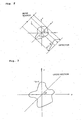
- Fig. 3 is a plan view showing the resulting state.
- a two-dimensional (2D) Fourier spectrum of cross sections of the specimen can be found by Fourier-transforming projections from all directions through the specimen and arraying the resulting spectra in a Fourier space.
- Cross-sectional images of the specimen can be obtained by inverse-Fourier transforming the 2D Fourier spectrum.
- a two-dimensional image (cross-sectional image) can be reconstructed from one-dimensional projections. Since a TEM image is a 2D projection, a three-dimensional image can be reconstructed simply by rotating the specimen along the axis of rotation.
- Fig. 4 is a perspective view illustrating the process for reconstructing a three-dimensional image. That is, a data array in a direction perpendicular to the axis of rotation is regarded as a 1D projection. A cross-sectional image is reconstructed from projections from various angles. A 3D image can be obtained by stacking 2D images obtained in this way along the axis of rotation.
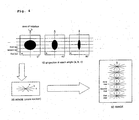
- a series of transmission images is obtained by tilting the specimen in incremental angular steps.
- the same field of view is selected and extracted from the series of transmission images by two-dimensional correlation processing. In this way, the problem of positional deviation of the specimen is solved.
- Fig. 5 is a front elevation illustrating the process for selecting and extracting the same field of view from a series of transmission images by two-dimensional correlation processing, the series of transmission images being obtained by tilting a specimen in incremental angular steps.
- two-dimensional correlation processing is performed between each obtained transmission image and a reference image.
- Parts of the transmission images which have the same field of view as the reference image are extracted from the transmission images at different angles.
- Computerized tomography is done using the extracted images.
- the reference image is obtained by extracting an image of a part of field of view from the transmission image obtained when the specimen stage is at some tilt angle (e.g., 0°).
- the accuracy at which transmission images are extracted by two-dimensional correlation processing can be improved by removing the trend in the transmission images (i.e., by removing first-order component or bias component).
- the reliability that the identified maximum value is a true maximum value is low. In this case, the reliability of the alignment (extraction of image) is deteriorated severely.
- cofEq. (9) or (10) described later is used, for example.
- c (i, j) ⁇ ⁇ f ⁇ x y ⁇ g ⁇ x - i , y - j ⁇ d x d y
- the degree of similarity is calculated in succession while translating the reference image within the image of interest. Because of the characteristics of the electronmicroscope, rotational movement is produced between the reference image and the image of interest.
- Eq. (9) is modified into Eq. (10) by adding a rotation through ⁇ within the xy plane with respect to a point within the image.
- This point within the image does not need to be the center of the image as long as it is a fixed point.
- c i j ⁇ ⁇ ⁇ ⁇ f ⁇ x y ⁇ g ⁇ x - i , y - j , ⁇ ⁇ d x d y d ⁇
- an image of a field of view that will become a reference image is extracted from a transmission image when the specimen stage is at some tilt angle (e.g., 0°). Then, 2D correlation processing is performed between the reference image and a transmission image derived when the specimen stage is at a different tilt angle. A field of view producing a maximum amount of correlation is extracted. The extracted field of view is rotated or tilted in the direction of ⁇ within the transmission image. Each such a field of view is multiplied with the reference image, and the total sum is taken. An image closest to the reference image can be obtained by adopting the maximum value of those values. That is, the rotation (tilt) in the direction of ⁇ within the transmission image is corrected. This processing is carried out repetitively. In consequence, images of the same field of view can be accurately extracted regarding transmission images at all tilt angles.
- some tilt angle e.g., 0°
- 2D correlation processing is performed between the reference image and a transmission image derived when the specimen stage is at a different tilt angle.
- an image extracted from the transmission image obtained when the specimen stage is at some tilt angle is not used for transmission images at all tilt angles . Rather, an image of the same field of view extracted from a transmission image at a different tilt angle using some reference image is used as a new reference image for 2D correlation processing between the reference image and a transmission image at a further tilt angle.
- Fig. 6 is a front elevation showing one example of process of performing 2D correlation processing using successively new reference images.
- an image of the same field of view is extracted from a transmission image obtained when the tilt angle of the stage is 30°.
- an image of the same field of view is extracted from a transmission image obtained when the tilt angle of the stage is 60° . Consequently, it is possible to avoid the problem that the difference in tilt angle of specimen stage between the reference image and the image to be processed is too large to perform the processing.
- the amount of deviation between the center of range in which a 3D image is reconstructed and the mechanical axis of rotation is added during back projection. This offers latitude in selecting a field of view. Therefore, an accurate reconstructed image is obtained.
- the amount of deviation can be found probabilistically from successive projection images. For example, the amount of deviation is optimized such that a good reconstructed image is obtained.
- the aforementioned problem is circumvented by taking the practically achievable maximum tilt angles of ⁇ 60° as recommended conditions for obtaining transmission images and adj usting the operating conditions under which 3D images are observed.
- two-dimensional correlation processing is performed between each of a series of transmission images obtained by tilting the specimen by plural angles and a reference image to thereby select and extract the same field of view. Positional deviation of the specimen is corrected. Therefore, an accurate 3D image can be reconstructed.
- the effects of the trend of the contrast of each transmission image are removed before the aforementioned two-dimensional correlation processing is performed. Consequently, the accuracy at which the transmission images are extracted by the 2D correlation processing can be improved.
- a certain decision criterion is established about the maximum value of the correlation results of the 2D correlation processing. Values not satisfying the criterion are not used as the results of the 2D correlation processing. Hence, the reliability of the correlation results of the 2D correlation processing can be secured.
- an image of the same field of view is extracted from a transmission image at a different tilt angle by the use of a reference image.
- the extracted image is used as a new reference image. 2D correlation processing is performed between this new reference image and a transmission image at a still other tilt angle.
- the amount of deviation between the center of the range of reconstruction of a 3D image and the mechanical axis of rotation is added during inverse Radon transform. This offers latitude in selecting a field of view.
- the present invention makes it possible to analyze the three-dimensional structure of a specimen without sectioning it, by making use of computerized tomography. Furthermore, problems intrinsically occurring when computerized tomography is applied to electron microscopy, i.e., limitations on the tilt angle of the specimen stage and problems associated with identification of the axis of rotation and rotation and shift of the image, are solved. As a result, an electron microscope that can utilize the computerized tomography in general cases can be offered.
Landscapes
- Chemical & Material Sciences (AREA)
- Analytical Chemistry (AREA)
- Analysing Materials By The Use Of Radiation (AREA)
- Length-Measuring Devices Using Wave Or Particle Radiation (AREA)
Claims (8)
- Microscope électronique (1) pour diriger un faisceau d'électrons vers un échantillon (S) supporté de manière inclinable et obtenir des images de TEM sur la base des électrons transmis à travers l'échantillon, le microscope étant équipé d'un circuit de traitement de signal (2) agencé pour effectuer une tomodensitométrie conformément aux données concernant les images de TEM obtenues de l'échantillon,
dans lequel ledit circuit de traitement de signal (2) est agencé pour :i) extraire les images du même champ de vision de chaque image d'une série d'images de TEM obtenues à partir de l'échantillon (S) incliné selon plusieurs angles par un traitement de corrélation bidimensionnelle entre chaque image de ladite série d'images de TEM et une image de référence,
caractérisé en ce que ledit circuit de traitement de signal (2) est en outre agencé pour :ii) corriger les rotations dans les images extraites ;iii) effectuer le calcul de tomodensitométrie sur la base des images extraites à rotation corrigée du même champ de vision ; etiv) retirer les effets de la tendance du contraste de chaque image de TEM avant l'exécution du traitement de corrélation bidimensionnelle. - Microscope électronique (1) selon la revendication 1, dans lequel ledit circuit de traitement de signal (2) est agencé pour utiliser un certain critère de décision concernant une valeur maximum des résultats de corrélation du traitement de corrélation bidimensionnelle et pour ne pas utiliser les valeurs ne satisfaisant pas au critère en tant que résultats du traitement de corrélation bidimensionnelle.
- Microscope électronique (1) selon l'une quelconque des revendications précédentes, dans lequel ledit circuit de traitement de signal (2) est agencé pour effectuer un traitement de corrélation bidimensionnelle entre une nouvelle image de référence et une image de TEM avec un autre angle d'inclinaison, la nouvelle image de référence étant une image du même champ de vision extraite d'une image de TEM avec un angle d'inclinaison différent en utilisant l'image de référence mentionnée en premier.
- Microscope électronique (1) selon l'une quelconque des revendications précédentes, dans lequel ledit circuit de traitement de signal (2) est agencé pour ajouter une quantité d'écart entre un centre d'une plage dans laquelle les images tridimensionnelles sont reconstruites et un centre mécanique d'axe lorsqu'une transformation de Radon inverse est effectuée.
- Procédé d'analyse d'une structure tridimensionnelle, en utilisant un microscope électronique (1) équipé d'un circuit de traitement de signal (2), le procédé comprenant les étapes consistant à :diriger un faisceau d'électrons vers un échantillon (S) supporté de manière inclinable ;obtenir des images de TEM sur la base des électrons transmis à travers l'échantillon ;effectuer une tomodensitométrie conformément aux données concernant les images de TEM obtenues de l'échantillon,dans lequel ledit circuit de traitement de signal (2) :i) extrait les images du même champ de vision de chaque image d'une série d'images de TEM obtenues à partir de l'échantillon (S) incliné selon plusieurs angles par un traitement de corrélation bidimensionnelle entre chaque image de ladite série d'images de TEM et une image de référence, caractérisé en ce que, en outre, ledit circuit de traitement de signal (2) :ii) corrige les rotations dans les images extraites ;iii) effectue le calcul de tomodensitométrie sur la base des images extraites à rotation corrigée du même champ de vision ; etiv) retire les effets de la tendance du contraste de chaque image de TEM avant l'exécution du traitement de corrélation bidimensionnelle.
- Procédé selon la revendication 5, dans lequel ledit circuit de traitement de signal (2) a un certain critère de décision concernant une valeur maximum des résultats de corrélation du traitement de corrélation bidimensionnelle et n'utilise pas les valeurs ne satisfaisant pas au critère en tant que résultats du traitement de corrélation bidimensionnelle.
- Procédé selon l'une quelconque des revendications 5 et 6, dans lequel ledit circuit de traitement de signal (2) effectue un traitement de corrélation bidimensionnelle entre une nouvelle image de référence et une image de TEM avec un autre angle d'inclinaison, la nouvelle image de référence étant une image du même champ de vision extraite d'une image de TEM avec un angle d'inclinaison différent en utilisant l'image de référence mentionnée en premier.
- Procédé selon l'une quelconque des revendications 5 à 7, dans lequel ledit circuit de traitement de signal (2) ajoute une quantité d'écart entre un centre d'une plage dans laquelle les images tridimensionnelles sont reconstruites et un centre mécanique d'axe lorsqu'une transformation de Radon inverse est effectuée.
Applications Claiming Priority (2)
| Application Number | Priority Date | Filing Date | Title |
|---|---|---|---|
| JP2003182739A JP2005019218A (ja) | 2003-06-26 | 2003-06-26 | 電子顕微鏡装置 |
| JP2003182739 | 2003-06-26 |
Publications (3)
| Publication Number | Publication Date |
|---|---|
| EP1492152A2 EP1492152A2 (fr) | 2004-12-29 |
| EP1492152A3 EP1492152A3 (fr) | 2008-03-19 |
| EP1492152B1 true EP1492152B1 (fr) | 2015-09-02 |
Family
ID=33411103
Family Applications (1)
| Application Number | Title | Priority Date | Filing Date |
|---|---|---|---|
| EP04253856.1A Expired - Lifetime EP1492152B1 (fr) | 2003-06-26 | 2004-06-28 | Microscope électronique |
Country Status (3)
| Country | Link |
|---|---|
| US (1) | US7064326B2 (fr) |
| EP (1) | EP1492152B1 (fr) |
| JP (1) | JP2005019218A (fr) |
Families Citing this family (17)
| Publication number | Priority date | Publication date | Assignee | Title |
|---|---|---|---|---|
| JP3813798B2 (ja) * | 2000-07-13 | 2006-08-23 | 株式会社日立製作所 | 電子顕微鏡 |
| JP4822920B2 (ja) * | 2006-04-27 | 2011-11-24 | 日本電子株式会社 | 3次元像構築方法および透過電子顕微鏡 |
| JP4538472B2 (ja) | 2007-03-15 | 2010-09-08 | 株式会社日立ハイテクノロジーズ | 画像形成方法、及び電子顕微鏡 |
| JP5309552B2 (ja) * | 2007-12-21 | 2013-10-09 | 富士通株式会社 | 電子線トモグラフィ法及び電子線トモグラフィ装置 |
| RU2010152658A (ru) * | 2008-05-23 | 2012-06-27 | Те Острейлиан Нэшнл Юниверсити (Au) | Обработка данных изображения |
| JP4988662B2 (ja) * | 2008-07-25 | 2012-08-01 | 株式会社日立ハイテクノロジーズ | 荷電粒子線装置 |
| JP5339368B2 (ja) * | 2009-09-18 | 2013-11-13 | 独立行政法人産業技術総合研究所 | 電子顕微鏡における三次元像構築画像処理方法 |
| JP5670096B2 (ja) * | 2009-11-17 | 2015-02-18 | 日本電子株式会社 | トモグラフィー法を用いた試料の3次元画像取得方法及び装置 |
| JP5331780B2 (ja) * | 2010-11-30 | 2013-10-30 | 株式会社日立ハイテクノロジーズ | 電子顕微鏡,電子顕微鏡用画像再構成システム、および電子顕微鏡用画像再構成方法 |
| JP5492115B2 (ja) * | 2011-02-10 | 2014-05-14 | 日本電子株式会社 | 電子顕微鏡用針状試料の作製方法 |
| USD708244S1 (en) * | 2012-11-30 | 2014-07-01 | Hitachi High-Technologies Corporation | Electron microscope |
| EP2916342A1 (fr) * | 2014-03-05 | 2015-09-09 | Fei Company | Fabrication d'une lamelle pour analyse tomographique corrélative avec résolution atomique |
| JP6272153B2 (ja) * | 2014-06-10 | 2018-01-31 | 株式会社日立ハイテクノロジーズ | 荷電粒子線装置、三次元画像の再構成画像処理システム、方法 |
| JP6796609B2 (ja) * | 2018-02-23 | 2020-12-09 | 日本電子株式会社 | 収差測定方法および電子顕微鏡 |
| CN109916928B (zh) * | 2019-03-15 | 2020-11-17 | 浙江大学 | 一种判断各向异性纳米晶体择优取向性组装结果的方法 |
| JP7369752B2 (ja) | 2021-10-13 | 2023-10-26 | 日本電子株式会社 | 電子顕微鏡及び電子顕微鏡の制御方法 |
| EP4206664A1 (fr) * | 2021-12-30 | 2023-07-05 | FEI Company | Procédés et systèmes d'imagerie par microscopie tomographique |
Family Cites Families (3)
| Publication number | Priority date | Publication date | Assignee | Title |
|---|---|---|---|---|
| JP3287858B2 (ja) * | 1991-05-15 | 2002-06-04 | 株式会社日立製作所 | 電子顕微鏡装置及び電子顕微方法 |
| US5866905A (en) * | 1991-05-15 | 1999-02-02 | Hitachi, Ltd. | Electron microscope |
| AU3267501A (en) * | 1999-11-02 | 2001-05-14 | Gary Greenberg | Tomographic microscope for high resolution imaging and method of analyzing specimens |
-
2003
- 2003-06-26 JP JP2003182739A patent/JP2005019218A/ja active Pending
-
2004
- 2004-06-24 US US10/876,300 patent/US7064326B2/en not_active Expired - Fee Related
- 2004-06-28 EP EP04253856.1A patent/EP1492152B1/fr not_active Expired - Lifetime
Also Published As
| Publication number | Publication date |
|---|---|
| EP1492152A2 (fr) | 2004-12-29 |
| JP2005019218A (ja) | 2005-01-20 |
| US7064326B2 (en) | 2006-06-20 |
| EP1492152A3 (fr) | 2008-03-19 |
| US20050029452A1 (en) | 2005-02-10 |
Similar Documents
| Publication | Publication Date | Title |
|---|---|---|
| EP1492152B1 (fr) | Microscope électronique | |
| EP0513776B1 (fr) | Instrument et procédé pour observer un arrangement tridimensional d'atomes | |
| Zaefferer | A critical review of orientation microscopy in SEM and TEM | |
| US5402460A (en) | Three-dimensional microtomographic analysis system | |
| EP1566766B1 (fr) | Procédé d'évaluation d'images et microscope | |
| EP2525386B1 (fr) | Microscopie à particules chargées avec détection d'occlusion | |
| US5422724A (en) | Multiple-scan method for wafer particle analysis | |
| Saghi et al. | Compressed sensing electron tomography of needle-shaped biological specimens–Potential for improved reconstruction fidelity with reduced dose | |
| US11636598B2 (en) | Imaging data processing apparatus and imaging data processing program to perform image alignment by deforming images such that imaged observation target sites coincide | |
| EP2652537B1 (fr) | Imagerie automatisée de zones prédéterminées dans des séries de coupes | |
| EP2648206B1 (fr) | Microscope électronique à transmission pour reconstruction de structures en trois dimensions, et procédé de reconstruction d'image pour microscope électronique à transmission | |
| Lassen | Automated determination of crystal orientations from electron backscattering patterns | |
| EP2966668A1 (fr) | Procédé d'étalonnage d'un microscope à particules chargées de transmission de balayage | |
| JP7138066B2 (ja) | 歳差電子回折データマッピングのために走査型透過電子顕微鏡を自動的にアライメントする方法 | |
| CN109142399A (zh) | 一种成像系统及样品探测方法 | |
| Guérin et al. | Targeted studies using serial block face and focused ion beam scan electron microscopy | |
| JP6876455B2 (ja) | 観察方法および試料作製方法 | |
| JP3304681B2 (ja) | 電子顕微鏡及び3次元原子配列観察方法 | |
| Zhang et al. | Large volume tomography using plasma FIB-SEM: A comprehensive case study on black silicon | |
| US11598732B2 (en) | Imaging system and method for specimen detection | |
| EP3392900B1 (fr) | Procédé d'alignement automatique d'un microscope électronique par transmission à balayage pour le mappage de données de diffraction d'électrons par précession | |
| Stegmann et al. | Characterization of barrier/seed layer stacks of Cu interconnects by electron tomographic three-dimensional object reconstruction | |
| CN109300087A (zh) | 提高样品切片的扫描成像在z轴方向上分辨率方法及系统 | |
| EP3474309B1 (fr) | Procédé de reconstruction d'image tridimensionnelle | |
| CN208420756U (zh) | 一种成像系统 |
Legal Events
| Date | Code | Title | Description |
|---|---|---|---|
| PUAI | Public reference made under article 153(3) epc to a published international application that has entered the european phase |
Free format text: ORIGINAL CODE: 0009012 |
|
| AK | Designated contracting states |
Kind code of ref document: A2 Designated state(s): AT BE BG CH CY CZ DE DK EE ES FI FR GB GR HU IE IT LI LU MC NL PL PT RO SE SI SK TR |
|
| AX | Request for extension of the european patent |
Extension state: AL HR LT LV MK |
|
| PUAL | Search report despatched |
Free format text: ORIGINAL CODE: 0009013 |
|
| AK | Designated contracting states |
Kind code of ref document: A3 Designated state(s): AT BE BG CH CY CZ DE DK EE ES FI FR GB GR HU IE IT LI LU MC NL PL PT RO SE SI SK TR |
|
| AX | Request for extension of the european patent |
Extension state: AL HR LT LV MK |
|
| 17P | Request for examination filed |
Effective date: 20080918 |
|
| AKX | Designation fees paid |
Designated state(s): DE NL |
|
| 17Q | First examination report despatched |
Effective date: 20110509 |
|
| GRAP | Despatch of communication of intention to grant a patent |
Free format text: ORIGINAL CODE: EPIDOSNIGR1 |
|
| INTG | Intention to grant announced |
Effective date: 20150316 |
|
| GRAS | Grant fee paid |
Free format text: ORIGINAL CODE: EPIDOSNIGR3 |
|
| GRAA | (expected) grant |
Free format text: ORIGINAL CODE: 0009210 |
|
| AK | Designated contracting states |
Kind code of ref document: B1 Designated state(s): DE NL |
|
| REG | Reference to a national code |
Ref country code: DE Ref legal event code: R096 Ref document number: 602004047797 Country of ref document: DE |
|
| REG | Reference to a national code |
Ref country code: NL Ref legal event code: FP |
|
| REG | Reference to a national code |
Ref country code: DE Ref legal event code: R097 Ref document number: 602004047797 Country of ref document: DE |
|
| PGFP | Annual fee paid to national office [announced via postgrant information from national office to epo] |
Ref country code: NL Payment date: 20160510 Year of fee payment: 13 |
|
| PLBE | No opposition filed within time limit |
Free format text: ORIGINAL CODE: 0009261 |
|
| STAA | Information on the status of an ep patent application or granted ep patent |
Free format text: STATUS: NO OPPOSITION FILED WITHIN TIME LIMIT |
|
| PGFP | Annual fee paid to national office [announced via postgrant information from national office to epo] |
Ref country code: DE Payment date: 20160622 Year of fee payment: 13 |
|
| 26N | No opposition filed |
Effective date: 20160603 |
|
| REG | Reference to a national code |
Ref country code: DE Ref legal event code: R119 Ref document number: 602004047797 Country of ref document: DE |
|
| REG | Reference to a national code |
Ref country code: NL Ref legal event code: MM Effective date: 20170701 |
|
| PG25 | Lapsed in a contracting state [announced via postgrant information from national office to epo] |
Ref country code: NL Free format text: LAPSE BECAUSE OF NON-PAYMENT OF DUE FEES Effective date: 20170701 |
|
| PG25 | Lapsed in a contracting state [announced via postgrant information from national office to epo] |
Ref country code: DE Free format text: LAPSE BECAUSE OF NON-PAYMENT OF DUE FEES Effective date: 20180103 |