EP1495497B1 - Detecteurs au germanium sensibles a la position comportant une microstructure sur les deux faces de contact - Google Patents
Detecteurs au germanium sensibles a la position comportant une microstructure sur les deux faces de contact Download PDFInfo
- Publication number
- EP1495497B1 EP1495497B1 EP03722394A EP03722394A EP1495497B1 EP 1495497 B1 EP1495497 B1 EP 1495497B1 EP 03722394 A EP03722394 A EP 03722394A EP 03722394 A EP03722394 A EP 03722394A EP 1495497 B1 EP1495497 B1 EP 1495497B1
- Authority
- EP
- European Patent Office
- Prior art keywords
- layer
- amorphous layer
- detector according
- spatially resolving
- amorphous
- Prior art date
- Legal status (The legal status is an assumption and is not a legal conclusion. Google has not performed a legal analysis and makes no representation as to the accuracy of the status listed.)
- Expired - Lifetime
Links
Images
Classifications
-
- H—ELECTRICITY
- H10—SEMICONDUCTOR DEVICES; ELECTRIC SOLID-STATE DEVICES NOT OTHERWISE PROVIDED FOR
- H10F—INORGANIC SEMICONDUCTOR DEVICES SENSITIVE TO INFRARED RADIATION, LIGHT, ELECTROMAGNETIC RADIATION OF SHORTER WAVELENGTH OR CORPUSCULAR RADIATION
- H10F30/00—Individual radiation-sensitive semiconductor devices in which radiation controls the flow of current through the devices, e.g. photodetectors
- H10F30/20—Individual radiation-sensitive semiconductor devices in which radiation controls the flow of current through the devices, e.g. photodetectors the devices having potential barriers, e.g. phototransistors
- H10F30/29—Individual radiation-sensitive semiconductor devices in which radiation controls the flow of current through the devices, e.g. photodetectors the devices having potential barriers, e.g. phototransistors the devices being sensitive to radiation having very short wavelengths, e.g. X-rays, gamma-rays or corpuscular radiation
-
- H—ELECTRICITY
- H10—SEMICONDUCTOR DEVICES; ELECTRIC SOLID-STATE DEVICES NOT OTHERWISE PROVIDED FOR
- H10F—INORGANIC SEMICONDUCTOR DEVICES SENSITIVE TO INFRARED RADIATION, LIGHT, ELECTROMAGNETIC RADIATION OF SHORTER WAVELENGTH OR CORPUSCULAR RADIATION
- H10F77/00—Constructional details of devices covered by this subclass
- H10F77/20—Electrodes
- H10F77/206—Electrodes for devices having potential barriers
Definitions
- the invention relates to a spatially resolving detector for the measurement of charged particles or photons. Furthermore, the invention relates to a tomograph or a Compton camera with such a detector.
- a detector of the type mentioned is the document " High Purity Germanium Position-Sensitive Detector for Positron Annihilation Experiments ", G. Riepe, D. Protlc, R. Kurz, W. Trifts Reifen, Z. Kajcsos and J. Winter, Proceedings 5th Int Conf. Positron Annihilation, (Japan , 1979 ) refer to. From this, a detector consisting of very pure crystalline germanium is known, which has been provided with microstructures on both sides. Phosphorus was implanted on one side of the detector and boron on the other side. Implantation was by ion implantation.
- a charged particle or photon When a charged particle or photon enters the detector, it generates electron-hole pairs in the region of the crystalline germanium. The respective charge migrates to the corresponding contact and is read out here. The locally measured charge represents a measure of the information sought.
- Boron-doped contacts in particular can be produced very easily by ion implantation.
- implanting with phosphorus is also a technically very simple process.
- radiation damage occurs which leads to p + doping in a layer which is supposed to represent an n or n + contact.
- the radiation damage is correspondingly disruptive.
- the n- or p-layers are provided with structures.
- the structures can be produced by a lithographic process. Lithographic techniques are common knowledge.
- a photosensitive resist is applied to the surface to be patterned in a photophotolithographic process. Through a mask, the photosensitive resist is partially exposed. By means of plasma etching trenches are then introduced into the surface at the exposed areas of the photoresist.
- the n-layer or p-layer is then structured. By this is meant that the layer acting as n- or p-contact is subdivided into individual segments separated by trenches. These separate elements are often referred to in the literature as location elements.
- the lacquer layer can be removed, for example, by chemical etching.
- the structuring can be strip-shaped on both sides. For example, the stripes on one side are then oriented perpendicular relative to the stripes on the other side, but in principle any geometric patterns are possible. So already a spiral-shaped structuring was provided on both sides. The spirals ran opposite, so that a spatial resolution was also possible.
- the thickness of the lithium layer which is typically 200 to 1000 ⁇ m deep, no transmission detectors can be disadvantageously provided.
- Aluminum may be replaced by other metals such as palladium or gold.
- the metal is structured and indeed applied in a strip.
- the amorphous germanium layer is not patterned. This is only very slightly conductive, so that the structuring of the metallic surface is sufficient to obtain a spatially resolving detector.
- the object of the invention is to provide a detector of the type mentioned above with improved accuracy in energy determination and improved energy resolution in the measurement.
- the object of the invention is achieved by a spatially resolving detector having the features of the first claim.
- Advantageous embodiments emerge from the subclaims.
- a method for producing the detector results from the independent claim.
- the structure of the metallic layer continues into the amorphous layer. It is therefore important in the invention that not only the metallic surface, but also the underlying amorphous layer is structured. The structures match.
- the structure of the metallic layer extends through the amorphous layer into the crystal structure, on which the amorphous layer is applied.
- the measurement accuracy in the energy determination is increased compared to the prior art, when the structuring extends into the amorphous layer.
- the achievable energy resolution is also significantly improved.
- the improvements succeed when the structure is passed through the amorphous layer and extends into the underlying crystalline structure. Only a few ⁇ m depth of the structure in the crystalline region is sufficient. At least 1 ⁇ m deep, preferably at least 5 ⁇ m deep, the structure should extend into the semiconducting region.
- the metallic layer may be made of aluminum, palladium or gold, for example.
- the crystalline region below the amorphous layer is then preferably also germanium.
- the structure is formed by segments, which have a distance of less than 200 microns, in particular a distance of less than 100 microns, more preferably less than 20 microns.
- the practically realizable lower limit is approx. 1 ⁇ m.
- the desired small structures can be produced for example by a photophotolfithographic method.
- the amorphous layer is basically applied to a semiconductor material.
- the amorphous layer therefore has an electrical conductivity which is substantially smaller than the conductivity of the material which is below the amorphous layer.
- an amorphous germanium layer is first sputtered on to crystalline germanium or vapor-deposited. Subsequently, a metal layer such as an aluminum layer is evaporated. Subsequently, the desired structures are produced in a defined manner lithographically. Within the amorphous germanium-metal layer, trenches are etched so deeply that they extend at least as far as the germanium crystal region. Advantageously, these trenches extend into the germanium crystal. On the opposite side, doping with boron and subsequent microstructuring provided the mating contact (p + ).
- the dimensions of a detector are typically 3 inches in diameter.
- the thickness of the detector is typically 10 to 20 mm.
- the effective thickness of the boron layer is regularly below 1 ⁇ m.
- the thickness of the amorphous germanium layer is typically about 0.1 ⁇ m thick.
- the metal layer is typically 0.1 to 0.2 ⁇ m thick.
- the depth of the trenches is typically 10 ⁇ m.
- implanted boron regularly reaches up to 10 ⁇ m or even up to 20 ⁇ m into the germanium crystal. It was also etched to this depth.
- the invention differs from the prior art in particular in that the depth of the trench reaches much further than would have been necessary for the metal layer or even for the amorphous germanium layer itself. This is essential to the invention in order to achieve the optimum effects.
- a crystal consisting of silicon may be provided instead of a germanium crystal.
- the detector is to be used in particular in the medical field because the detectors used hitherto do not provide the required spatial resolutions while at the same time having a high counting rate.
- the spatial resolution can be increased virtually unlimited in the present invention. In terms of order of magnitude, the spatial resolution can easily be doubled in comparison with the previously used in medical detectors while maintaining the remaining performance.
- the spatial resolution in the medical field was previously 2 mm. Local resolutions of 1 mm can now be realized without any problems. Especially in the field of tomography, the detector is used to achieve much better results.
- Positron emission tomography is another area in the medical field where the detector can be used to advantage.
- SPECT is another application example.
- the detector is then in particular part of a Compton camera.
- Small animal positron emission tomography is another typical application example in medicine.
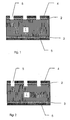
- FIG. 1 shows a section through a semiconductor consisting of germanium 1.
- the semiconductor 1 has on a surface on a layer 2, which consists of amorphous germanium. This forms an n + contact.
- Opposite is a layer 3 of the semiconductor doped with boron. This forms a p + contact.
- metallic layers 4 and 5 are applied, which serve the electrical contact.
- the metallic layer is structurally patterned on the side with the n + contact. Instead, the trenches 5 to 5 extend into the amorphous layer 2 so that they have individual segments separated from one another.
- the p + contact may also be structured like a stripe.
- the strips then run basically perpendicular to the strips on the side with the amorphous germanium (here parallel to the paper plane). Therefore, no trenches are visible.
- the trenches 5 extend into the semiconductor material.
- germanium for example, crystalline or amorphous silicon can be used.
- Suitable semiconductor materials are III-V compounds such as GaAs or CdTe.
- doping with boron it has been found that the layer 3 can be replaced by amorphous germanium or even amorphous silicon. Why this works is not physically clear.
- the width of the trenches are between 1 and 200 microns.
- the strips are thus 1 and 200 microns apart.
Landscapes
- Measurement Of Radiation (AREA)
- Light Receiving Elements (AREA)
- Pressure Sensors (AREA)
Claims (9)
- Détecteur sensible à la position pour la mesure de particules chargées ou de photons avec une zone superficielle qui est formée par une couche amorphe (2) et une couche métallique (4), structurée se trouvant dessus, avec une zone cristalline (1) au-dessous de la couche amorphe, caractérisé en ce que la structure (5) de la couche métallique est poursuivie dans la couche amorphe (2) de sorte que la structure (5) dans la couche amorphe (2) concorde avec la structure (5) dans la couche métallique.
- Détecteur sensible à la position selon la revendication 1, caractérisé en ce que la structure de la couche métallique parvient au travers de la couche amorphe jusque dans la structure cristalline, sur laquelle est appliquée la couche amorphe.
- Détecteur sensible à la position selon la revendication 1 ou 2, caractérisé en ce que la couche amorphe est constituée de germanium ou de silicium.
- Détecteur sensible à la position selon l'une quelconque des revendications précédentes, caractérisé en ce que la couche métallique se compose d'aluminium, de palladium ou d'or.
- Détecteur sensible à la position selon l'une quelconque des revendications précédentes, caractérisé en ce que la zone cristalline au-dessous de la couche amorphe est constituée de germanium, de silicium ou d'une combinaison III-V.
- Détecteur sensible à la position selon l'une quelconque des revendications précédentes, caractérisé en ce que la structure est constituée de segments qui présentent entre eux une distance inférieure à 200 µm, en particulier une distance inférieure à 100 µm, de manière particulièrement préférée inférieure à 20 µm.
- Détecteur sensible à la position selon l'une quelconque des revendications précédentes, caractérisé en ce que la couche amorphe est appliquée sur un matériau semi-conducteur.
- Détecteur sensible à la position selon l'une quelconque des revendications précédentes, caractérisé en ce que la couche amorphe présente une conductibilité électrique qui est essentiellement inférieure à la conductibilité du matériau qui se trouve au-dessous de la couche amorphe.
- Tomographe ou caméra Compton dotée d'un détecteur selon l'une quelconque des revendications précédentes.
Applications Claiming Priority (3)
| Application Number | Priority Date | Filing Date | Title |
|---|---|---|---|
| DE10217426A DE10217426B4 (de) | 2002-04-18 | 2002-04-18 | Ortsauflösender Detektor für die Messung elektrisch geladener Teilchen und Verwendung des Detektors |
| DE10217426 | 2002-04-18 | ||
| PCT/EP2003/003485 WO2003088368A2 (fr) | 2002-04-18 | 2003-04-03 | Detecteurs au germanium sensibles a la position comportant une microstructure sur les deux faces de contact |
Publications (2)
| Publication Number | Publication Date |
|---|---|
| EP1495497A2 EP1495497A2 (fr) | 2005-01-12 |
| EP1495497B1 true EP1495497B1 (fr) | 2008-10-29 |
Family
ID=29224575
Family Applications (1)
| Application Number | Title | Priority Date | Filing Date |
|---|---|---|---|
| EP03722394A Expired - Lifetime EP1495497B1 (fr) | 2002-04-18 | 2003-04-03 | Detecteurs au germanium sensibles a la position comportant une microstructure sur les deux faces de contact |
Country Status (6)
| Country | Link |
|---|---|
| US (1) | US20050230627A1 (fr) |
| EP (1) | EP1495497B1 (fr) |
| JP (1) | JP4681233B2 (fr) |
| AT (1) | ATE412977T1 (fr) |
| DE (2) | DE10217426B4 (fr) |
| WO (1) | WO2003088368A2 (fr) |
Families Citing this family (7)
| Publication number | Priority date | Publication date | Assignee | Title |
|---|---|---|---|---|
| WO2007031886A2 (fr) * | 2005-09-15 | 2007-03-22 | Koninklijke Philips Electronics N.V. | Detecteurs transistorises presentant des performances ameliorees |
| CA2541256A1 (fr) * | 2006-02-22 | 2007-08-22 | Redlen Technologies Inc. | Electrode de protection pour detecteur monolithique de rayonnement |
| US8785865B2 (en) | 2008-12-03 | 2014-07-22 | Tohoku University | Semiconductor detector for two-dimensionally detecting radiation positions and method for two-dimensionally detecting radiation positions using the same |
| US8476101B2 (en) * | 2009-12-28 | 2013-07-02 | Redlen Technologies | Method of fabricating patterned CZT and CdTe devices |
| JP2014239152A (ja) | 2013-06-07 | 2014-12-18 | シーメンス アクチエンゲゼルシヤフトSiemens Aktiengesellschaft | 電極層を分断する溝を有する半導体素子及びその溝の形成方法 |
| US9864138B2 (en) | 2015-01-05 | 2018-01-09 | The Research Foundation For The State University Of New York | Integrated photonics including germanium |
| EP3362819A4 (fr) * | 2015-10-14 | 2019-06-05 | Shenzhen Xpectvision Technology Co., Ltd. | Détecteurs de rayons x aptes à limiter la diffusion de porteurs de charge |
Family Cites Families (17)
| Publication number | Priority date | Publication date | Assignee | Title |
|---|---|---|---|---|
| JPS603792B2 (ja) * | 1977-02-04 | 1985-01-30 | 株式会社東芝 | マルチチヤネル型半導体放射線検出器 |
| JPS57154083A (en) * | 1981-03-19 | 1982-09-22 | Yokogawa Hokushin Electric Corp | Ct scanner |
| JPS60124879A (ja) * | 1983-12-08 | 1985-07-03 | Yokogawa Hokushin Electric Corp | 多チャンネル形放射線検出器及びその製造方法 |
| JPH0816702B2 (ja) * | 1983-12-26 | 1996-02-21 | 株式会社島津製作所 | 半導体放射線位置検出装置 |
| JPS61196572A (ja) * | 1985-02-25 | 1986-08-30 | Hitachi Zosen Corp | アモルフアスシリコンx線センサ |
| JPS6412582A (en) * | 1987-07-07 | 1989-01-17 | Matsushita Electric Industrial Co Ltd | Semiconductor radiation detector |
| JPH0221284A (ja) * | 1988-07-08 | 1990-01-24 | Matsushita Electric Ind Co Ltd | 粒子線検出装置 |
| US5164809A (en) * | 1989-04-21 | 1992-11-17 | The Regents Of The University Of Calif. | Amorphous silicon radiation detectors |
| EP0597943A4 (en) * | 1991-07-31 | 1994-07-27 | Univ California | Improvements in particle detector spatial resolution. |
| JP3036258B2 (ja) * | 1992-10-08 | 2000-04-24 | 富士電機株式会社 | 半導体放射線検出器 |
| JPH06260671A (ja) * | 1993-03-09 | 1994-09-16 | Japan Energy Corp | 半導体放射線検出器およびその製造方法 |
| WO1994025878A1 (fr) * | 1993-04-28 | 1994-11-10 | University Of Surrey | Detecteurs de radiations |
| FR2757685B1 (fr) * | 1996-12-24 | 1999-05-14 | Commissariat Energie Atomique | Dispositif de detection de rayonnements ionisants a semi-conducteur de haute resistivite |
| US6175120B1 (en) * | 1998-05-08 | 2001-01-16 | The Regents Of The University Of Michigan | High-resolution ionization detector and array of such detectors |
| US6069360A (en) * | 1998-05-08 | 2000-05-30 | Lund; James C. | Method and apparatus for electron-only radiation detectors from semiconductor materials |
| JP2000121738A (ja) * | 1998-10-20 | 2000-04-28 | Hitachi Medical Corp | 半導体放射線検出器 |
| JP2001274450A (ja) * | 2000-03-23 | 2001-10-05 | Fuji Electric Co Ltd | β線検出器 |
-
2002
- 2002-04-18 DE DE10217426A patent/DE10217426B4/de not_active Expired - Fee Related
-
2003
- 2003-04-03 AT AT03722394T patent/ATE412977T1/de active
- 2003-04-03 JP JP2003585191A patent/JP4681233B2/ja not_active Expired - Fee Related
- 2003-04-03 DE DE50310702T patent/DE50310702D1/de not_active Expired - Lifetime
- 2003-04-03 US US10/511,734 patent/US20050230627A1/en not_active Abandoned
- 2003-04-03 EP EP03722394A patent/EP1495497B1/fr not_active Expired - Lifetime
- 2003-04-03 WO PCT/EP2003/003485 patent/WO2003088368A2/fr not_active Ceased
Also Published As
| Publication number | Publication date |
|---|---|
| US20050230627A1 (en) | 2005-10-20 |
| JP4681233B2 (ja) | 2011-05-11 |
| DE50310702D1 (de) | 2008-12-11 |
| WO2003088368A3 (fr) | 2004-02-05 |
| ATE412977T1 (de) | 2008-11-15 |
| DE10217426A1 (de) | 2003-11-13 |
| JP2005523438A (ja) | 2005-08-04 |
| DE10217426B4 (de) | 2006-09-14 |
| WO2003088368A2 (fr) | 2003-10-23 |
| EP1495497A2 (fr) | 2005-01-12 |
Similar Documents
| Publication | Publication Date | Title |
|---|---|---|
| DE102016106119B4 (de) | Energiefilterelement für Ionenimplantationsanlagen für den Einsatz in der Produktion von Wafern | |
| EP1468309B1 (fr) | Detecteur concu pour detecter des faisceaux de particules et procede de fabrication dudit detecteur | |
| DE69518986T2 (de) | Detektor für ionisierende strahlung | |
| DE19532415A1 (de) | Neutronendetektor | |
| DE10392637T5 (de) | Hintergrundbeleuchtetes Photodioden-Array und Verfahren zum Herstellen desselben | |
| EP0698910A2 (fr) | Procédé et dispositif détecteur pourla détection électronique spatiale de rayonnement | |
| WO2007022862A2 (fr) | Procede de fabrication d'un ensemble lentilles electrostatique a plusieurs couches | |
| DE19708766C2 (de) | Lithographiemaske und Verfahren zur Herstellung derselben | |
| DE60033509T2 (de) | Zweidimensionaler detektor für ionisierende strahlung und zugehöriges herstellungsverfahren | |
| EP1495497B1 (fr) | Detecteurs au germanium sensibles a la position comportant une microstructure sur les deux faces de contact | |
| DE102015114374B4 (de) | Gammastrahlendetektor und verfahren zur detektion von gammastrahlen | |
| DE102011089776B4 (de) | Detektorelement, Strahlungsdetektor, medizinisches Gerät und Verfahren zum Erzeugen eines solchen Detektorelements | |
| DE4310622A1 (de) | Einrichtung zur Mikrobilderzeugung mittels ionisierender Strahlung | |
| DE3446208A1 (de) | Ionisationsdetektor und verfahren zum verbessern des stromverhaltens von dessen detektorelementen | |
| DE202017007025U1 (de) | Ionisierungsstrahlungssensor auf Basis des im Zonen-Floating-Verfahren erhaltenen Siliziums mit N-Typ-Leitfähigkeit | |
| DE102009015563A1 (de) | Röntgenstrahlungsdetektor zur Detektion von ionisierender Strahlung, insbesondere zur Verwendung in einem CT-System | |
| DE3446207A1 (de) | Ionisationsdetektorgehaeuse, verfahren zu seiner herstellung und damit ausgeruesteter strahlungsdetektor | |
| EP1399977B1 (fr) | Detecteur de position microstructure bilateral | |
| DE10255605B4 (de) | Reflektionsmaske zur Projektion einer Struktur auf einen Halbleiterwafer sowie Verfahren zu deren Herstellung | |
| DE3878339T2 (de) | Detektor fuer ionisierende teilchen. | |
| EP0156024B1 (fr) | Système de détection | |
| DE2721912A1 (de) | Verfahren zur herstellung von halbleitereinrichtungen, insbesondere dioden und thyristoren | |
| DE69626547T2 (de) | Ultradünner detektor für ionisierende strahlung und verfahren zur herstellung | |
| DE102016015819B3 (de) | Verfahren zur Ionenimplantation | |
| DE102016015822B3 (de) | Verfahren zur Ionenimplantation |
Legal Events
| Date | Code | Title | Description |
|---|---|---|---|
| PUAI | Public reference made under article 153(3) epc to a published international application that has entered the european phase |
Free format text: ORIGINAL CODE: 0009012 |
|
| 17P | Request for examination filed |
Effective date: 20040812 |
|
| AK | Designated contracting states |
Kind code of ref document: A2 Designated state(s): AT BE BG CH CY CZ DE DK EE ES FI FR GB GR HU IE IT LI LU MC NL PT RO SE SI SK TR |
|
| 17Q | First examination report despatched |
Effective date: 20070820 |
|
| R17C | First examination report despatched (corrected) |
Effective date: 20071022 |
|
| GRAP | Despatch of communication of intention to grant a patent |
Free format text: ORIGINAL CODE: EPIDOSNIGR1 |
|
| GRAS | Grant fee paid |
Free format text: ORIGINAL CODE: EPIDOSNIGR3 |
|
| GRAA | (expected) grant |
Free format text: ORIGINAL CODE: 0009210 |
|
| AK | Designated contracting states |
Kind code of ref document: B1 Designated state(s): AT BE BG CH CY CZ DE DK EE ES FI FR GB GR HU IE IT LI LU MC NL PT RO SE SI SK TR |
|
| REG | Reference to a national code |
Ref country code: GB Ref legal event code: FG4D Free format text: NOT ENGLISH |
|
| REG | Reference to a national code |
Ref country code: CH Ref legal event code: EP |
|
| REG | Reference to a national code |
Ref country code: IE Ref legal event code: FG4D Free format text: LANGUAGE OF EP DOCUMENT: GERMAN |
|
| REF | Corresponds to: |
Ref document number: 50310702 Country of ref document: DE Date of ref document: 20081211 Kind code of ref document: P |
|
| NLV1 | Nl: lapsed or annulled due to failure to fulfill the requirements of art. 29p and 29m of the patents act | ||
| PG25 | Lapsed in a contracting state [announced via postgrant information from national office to epo] |
Ref country code: BG Free format text: LAPSE BECAUSE OF FAILURE TO SUBMIT A TRANSLATION OF THE DESCRIPTION OR TO PAY THE FEE WITHIN THE PRESCRIBED TIME-LIMIT Effective date: 20090129 Ref country code: ES Free format text: LAPSE BECAUSE OF FAILURE TO SUBMIT A TRANSLATION OF THE DESCRIPTION OR TO PAY THE FEE WITHIN THE PRESCRIBED TIME-LIMIT Effective date: 20090209 |
|
| PG25 | Lapsed in a contracting state [announced via postgrant information from national office to epo] |
Ref country code: FI Free format text: LAPSE BECAUSE OF FAILURE TO SUBMIT A TRANSLATION OF THE DESCRIPTION OR TO PAY THE FEE WITHIN THE PRESCRIBED TIME-LIMIT Effective date: 20081029 Ref country code: PT Free format text: LAPSE BECAUSE OF FAILURE TO SUBMIT A TRANSLATION OF THE DESCRIPTION OR TO PAY THE FEE WITHIN THE PRESCRIBED TIME-LIMIT Effective date: 20090330 Ref country code: SI Free format text: LAPSE BECAUSE OF FAILURE TO SUBMIT A TRANSLATION OF THE DESCRIPTION OR TO PAY THE FEE WITHIN THE PRESCRIBED TIME-LIMIT Effective date: 20081029 Ref country code: NL Free format text: LAPSE BECAUSE OF FAILURE TO SUBMIT A TRANSLATION OF THE DESCRIPTION OR TO PAY THE FEE WITHIN THE PRESCRIBED TIME-LIMIT Effective date: 20081029 |
|
| REG | Reference to a national code |
Ref country code: IE Ref legal event code: FD4D |
|
| PG25 | Lapsed in a contracting state [announced via postgrant information from national office to epo] |
Ref country code: IE Free format text: LAPSE BECAUSE OF FAILURE TO SUBMIT A TRANSLATION OF THE DESCRIPTION OR TO PAY THE FEE WITHIN THE PRESCRIBED TIME-LIMIT Effective date: 20081029 Ref country code: RO Free format text: LAPSE BECAUSE OF FAILURE TO SUBMIT A TRANSLATION OF THE DESCRIPTION OR TO PAY THE FEE WITHIN THE PRESCRIBED TIME-LIMIT Effective date: 20081029 Ref country code: EE Free format text: LAPSE BECAUSE OF FAILURE TO SUBMIT A TRANSLATION OF THE DESCRIPTION OR TO PAY THE FEE WITHIN THE PRESCRIBED TIME-LIMIT Effective date: 20081029 Ref country code: DK Free format text: LAPSE BECAUSE OF FAILURE TO SUBMIT A TRANSLATION OF THE DESCRIPTION OR TO PAY THE FEE WITHIN THE PRESCRIBED TIME-LIMIT Effective date: 20081029 |
|
| PG25 | Lapsed in a contracting state [announced via postgrant information from national office to epo] |
Ref country code: CZ Free format text: LAPSE BECAUSE OF FAILURE TO SUBMIT A TRANSLATION OF THE DESCRIPTION OR TO PAY THE FEE WITHIN THE PRESCRIBED TIME-LIMIT Effective date: 20081029 Ref country code: SE Free format text: LAPSE BECAUSE OF FAILURE TO SUBMIT A TRANSLATION OF THE DESCRIPTION OR TO PAY THE FEE WITHIN THE PRESCRIBED TIME-LIMIT Effective date: 20090129 Ref country code: IT Free format text: LAPSE BECAUSE OF FAILURE TO SUBMIT A TRANSLATION OF THE DESCRIPTION OR TO PAY THE FEE WITHIN THE PRESCRIBED TIME-LIMIT Effective date: 20081029 |
|
| PLBE | No opposition filed within time limit |
Free format text: ORIGINAL CODE: 0009261 |
|
| STAA | Information on the status of an ep patent application or granted ep patent |
Free format text: STATUS: NO OPPOSITION FILED WITHIN TIME LIMIT |
|
| PG25 | Lapsed in a contracting state [announced via postgrant information from national office to epo] |
Ref country code: SK Free format text: LAPSE BECAUSE OF FAILURE TO SUBMIT A TRANSLATION OF THE DESCRIPTION OR TO PAY THE FEE WITHIN THE PRESCRIBED TIME-LIMIT Effective date: 20081029 |
|
| 26N | No opposition filed |
Effective date: 20090730 |
|
| REG | Reference to a national code |
Ref country code: CH Ref legal event code: PL |
|
| PG25 | Lapsed in a contracting state [announced via postgrant information from national office to epo] |
Ref country code: LI Free format text: LAPSE BECAUSE OF NON-PAYMENT OF DUE FEES Effective date: 20090430 Ref country code: CH Free format text: LAPSE BECAUSE OF NON-PAYMENT OF DUE FEES Effective date: 20090430 |
|
| PG25 | Lapsed in a contracting state [announced via postgrant information from national office to epo] |
Ref country code: MC Free format text: LAPSE BECAUSE OF NON-PAYMENT OF DUE FEES Effective date: 20090430 |
|
| PG25 | Lapsed in a contracting state [announced via postgrant information from national office to epo] |
Ref country code: GR Free format text: LAPSE BECAUSE OF FAILURE TO SUBMIT A TRANSLATION OF THE DESCRIPTION OR TO PAY THE FEE WITHIN THE PRESCRIBED TIME-LIMIT Effective date: 20090130 |
|
| PG25 | Lapsed in a contracting state [announced via postgrant information from national office to epo] |
Ref country code: LU Free format text: LAPSE BECAUSE OF NON-PAYMENT OF DUE FEES Effective date: 20090403 |
|
| PG25 | Lapsed in a contracting state [announced via postgrant information from national office to epo] |
Ref country code: HU Free format text: LAPSE BECAUSE OF FAILURE TO SUBMIT A TRANSLATION OF THE DESCRIPTION OR TO PAY THE FEE WITHIN THE PRESCRIBED TIME-LIMIT Effective date: 20090430 |
|
| PG25 | Lapsed in a contracting state [announced via postgrant information from national office to epo] |
Ref country code: TR Free format text: LAPSE BECAUSE OF FAILURE TO SUBMIT A TRANSLATION OF THE DESCRIPTION OR TO PAY THE FEE WITHIN THE PRESCRIBED TIME-LIMIT Effective date: 20081029 |
|
| PG25 | Lapsed in a contracting state [announced via postgrant information from national office to epo] |
Ref country code: CY Free format text: LAPSE BECAUSE OF FAILURE TO SUBMIT A TRANSLATION OF THE DESCRIPTION OR TO PAY THE FEE WITHIN THE PRESCRIBED TIME-LIMIT Effective date: 20081029 |
|
| REG | Reference to a national code |
Ref country code: FR Ref legal event code: PLFP Year of fee payment: 13 |
|
| PGFP | Annual fee paid to national office [announced via postgrant information from national office to epo] |
Ref country code: DE Payment date: 20150311 Year of fee payment: 13 Ref country code: GB Payment date: 20150423 Year of fee payment: 13 |
|
| PGFP | Annual fee paid to national office [announced via postgrant information from national office to epo] |
Ref country code: FR Payment date: 20150422 Year of fee payment: 13 Ref country code: BE Payment date: 20150430 Year of fee payment: 13 Ref country code: AT Payment date: 20150422 Year of fee payment: 13 |
|
| PG25 | Lapsed in a contracting state [announced via postgrant information from national office to epo] |
Ref country code: BE Free format text: LAPSE BECAUSE OF NON-PAYMENT OF DUE FEES Effective date: 20160430 |
|
| REG | Reference to a national code |
Ref country code: DE Ref legal event code: R119 Ref document number: 50310702 Country of ref document: DE |
|
| REG | Reference to a national code |
Ref country code: AT Ref legal event code: MM01 Ref document number: 412977 Country of ref document: AT Kind code of ref document: T Effective date: 20160403 |
|
| GBPC | Gb: european patent ceased through non-payment of renewal fee |
Effective date: 20160403 |
|
| REG | Reference to a national code |
Ref country code: FR Ref legal event code: ST Effective date: 20161230 |
|
| PG25 | Lapsed in a contracting state [announced via postgrant information from national office to epo] |
Ref country code: DE Free format text: LAPSE BECAUSE OF NON-PAYMENT OF DUE FEES Effective date: 20161101 Ref country code: GB Free format text: LAPSE BECAUSE OF NON-PAYMENT OF DUE FEES Effective date: 20160403 Ref country code: FR Free format text: LAPSE BECAUSE OF NON-PAYMENT OF DUE FEES Effective date: 20160502 |
|
| PG25 | Lapsed in a contracting state [announced via postgrant information from national office to epo] |
Ref country code: AT Free format text: LAPSE BECAUSE OF NON-PAYMENT OF DUE FEES Effective date: 20160403 |