EP1502123B1 - Procede et dispositif pour tester des cartes de circuits imprimes et sonde de test associee - Google Patents
Procede et dispositif pour tester des cartes de circuits imprimes et sonde de test associee Download PDFInfo
- Publication number
- EP1502123B1 EP1502123B1 EP03725115A EP03725115A EP1502123B1 EP 1502123 B1 EP1502123 B1 EP 1502123B1 EP 03725115 A EP03725115 A EP 03725115A EP 03725115 A EP03725115 A EP 03725115A EP 1502123 B1 EP1502123 B1 EP 1502123B1
- Authority
- EP
- European Patent Office
- Prior art keywords
- circuit board
- test
- tested
- probe
- contact tip
- Prior art date
- Legal status (The legal status is an assumption and is not a legal conclusion. Google has not performed a legal analysis and makes no representation as to the accuracy of the status listed.)
- Expired - Lifetime
Links
Images




Classifications
-
- G—PHYSICS
- G01—MEASURING; TESTING
- G01R—MEASURING ELECTRIC VARIABLES; MEASURING MAGNETIC VARIABLES
- G01R31/00—Arrangements for testing electric properties; Arrangements for locating electric faults; Arrangements for electrical testing characterised by what is being tested not provided for elsewhere
- G01R31/28—Testing of electronic circuits, e.g. by signal tracer
-
- G—PHYSICS
- G01—MEASURING; TESTING
- G01R—MEASURING ELECTRIC VARIABLES; MEASURING MAGNETIC VARIABLES
- G01R31/00—Arrangements for testing electric properties; Arrangements for locating electric faults; Arrangements for electrical testing characterised by what is being tested not provided for elsewhere
- G01R31/28—Testing of electronic circuits, e.g. by signal tracer
- G01R31/2801—Testing of printed circuits, backplanes, motherboards, hybrid circuits or carriers for multichip packages [MCP]
- G01R31/2806—Apparatus therefor, e.g. test stations, drivers, analysers, conveyors
- G01R31/2808—Holding, conveying or contacting devices, e.g. test adapters, edge connectors, extender boards
-
- G—PHYSICS
- G01—MEASURING; TESTING
- G01R—MEASURING ELECTRIC VARIABLES; MEASURING MAGNETIC VARIABLES
- G01R1/00—Details of instruments or arrangements of the types included in groups G01R5/00 - G01R13/00 and G01R31/00
- G01R1/02—General constructional details
- G01R1/06—Measuring leads; Measuring probes
- G01R1/067—Measuring probes
-
- G—PHYSICS
- G01—MEASURING; TESTING
- G01R—MEASURING ELECTRIC VARIABLES; MEASURING MAGNETIC VARIABLES
- G01R1/00—Details of instruments or arrangements of the types included in groups G01R5/00 - G01R13/00 and G01R31/00
- G01R1/02—General constructional details
- G01R1/06—Measuring leads; Measuring probes
- G01R1/067—Measuring probes
- G01R1/06794—Devices for sensing when probes are in contact, or in position to contact, with measured object
Definitions
- the present invention relates to a device and a method for testing printed circuit boards, as well as a test probe for this device and this method.
- Testers for testing printed circuit boards can basically be divided into two groups, those with finger testers and parallel testers.
- the parallel testers are testers that simultaneously contact all or at least most of the board test points of a printed circuit board to be tested by means of an adapter.
- Finger testers are test devices for testing unpopulated or populated printed circuit boards, which scan the individual contact points sequentially or serially with two or more test fingers. Serial testing with a finger tester is inherently slower than parallel testing with a parallel tester.
- test fingers are usually attached to a carriage, which is movable along trusses, the trusses are again guided and movable on guide rails.
- the slides can thus be positioned at any point of a generally rectangular test field.
- testing devices with stationary cross members on which carriages are designed to be movable.
- On this slide test fingers are arranged, which have a certain length and are pivotally mounted at one end to the carriage. Due to the pivoting movement of the test finger, a certain area can be scanned across the traverse. Both types of finger testers can be used to contact and test all PCB test points on a circuit board under test.
- a finger tester in EP 0 468 153 A1 and a method for testing printed circuit boards by means of a finger tester are described in EP 0 853 242 A1.
- the essential criterion for successful implementation of finger testers on the market is the speed at which a printed circuit board to be tested can be tested.
- special test methods eg EP 0 853 242 A1 or the corresponding US 5,977,776
- special test probes eg US 5,804,982 or US 6,344,751
- Such a test probe for quickly contacting a circuit board test point of a printed circuit board to be tested is shown in US 5,113,133.
- a calibration plate which is a large-area printed circuit board, on which by means of the conductor tracks a grid is formed on the surface of the printed circuit board, is inserted into the test device.
- the individual conductor tracks are arranged at a distance of, for example, 1 to 3 cm from each other. Alone in the edge region of this calibration plate, a very wide conductor track is formed, which is in electrical contact with all other conductor tracks.
- one of the test fingers is placed on the wide conductor track, and with another test finger, the crossing points of the grid are scanned.
- the coordinates of the test finger or the slide are stored and correlated with the coordinates of the corresponding crossing point of the calibration plate (eg US 48 20 975).
- the locating of the individual intersection points takes place by a stepwise approach to the intersection point, until a conductive connection is established via the two contact fingers and the conductor tracks of the calibration plate. This step-like approach can be carried out, for example, circular or spiral.
- the test finger is placed on the calibration plate lowered and then raised again. To find a grid point, a few ten sample measurements may be necessary. If all grid points of the calibration plate have been successfully detected, different correction values for driving the test fingers of the test device are determined and stored for individual regions of the test area. These correction or calibration values allow a test finger in a coordinate system of the test direction to be precisely controlled and placed in the test area.
- the second calibration procedure is usually carried out for each circuit board to be tested.
- the printed circuit board of the batch is inserted into the test apparatus and then striking printed circuit board test points of the sample of printed circuit board test points to be tested are detected by means of the test fingers and their position in the test apparatus determined.
- the CAD data of the board test points of the board to be tested may be brought into correspondence with the physical board coordinates, that is, the warp delays and offsets of the pattern of the board test points are captured.
- the printed circuit board test points of the circuit board to be tested can be successfully activated and contacted by means of the test fingers.
- the first calibration procedure is necessary every time the test apparatus is reset, e.g. Example, when a test finger is replaced or if the tester is redesigned at the beginning of a working day.
- the first calibration procedure is also performed each time the ambient temperature changes by, for example, more than 3 ° C.
- an image acquisition system for a device for testing printed circuit boards emerges. Similar to an X-Y-recorder, this image acquisition system has a movable traverse on which a test head with a vertically movable test needle is arranged. In addition to the test needle, an image acquisition device consisting of a lens and a CCD element is arranged. The image generated by the image acquisition device is displayed on a monitor. An operator can use the image displayed on the screen to control the test head in such a way that, during a learning phase, it exits all the contact points to be tested and programs the corresponding coordinates. During the test, the device automatically moves the individual contact points and contacts them with the test needle.
- the invention has for its object to provide a device and a method for testing printed circuit boards by means of test fingers, with which the reliability of contacting printed circuit board test points can be increased with less calibration effort compared to conventional finger tester.
- the invention has for its object to provide a test probe for this device and this method.
- the object is achieved by a device having the features of claim 1, a method having the features of claim 11 and a test probe having the features of claim 18.
- the contact points are monitored during the testing process by means of an optical detection device and their movement is corrected automatically at least when starting a part of the board test points of a printed circuit board to be tested by means of the result determined by the optical detection means such that the contact tip securely contacts the respective board test point.
- the contact tip securely contacts the respective board test point.
- Calibration data can be calculated from the resulting correction data.
- the calibration process is carried out together with the actual testing or measuring process, without this being significantly delayed. This represents a significant acceleration of the method of testing printed circuit boards by means of a finger tester and considerably increases the throughput of printed circuit boards to be tested.
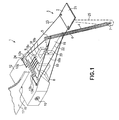
- FIGS. 1 and 2 show two different exemplary embodiments of test probes 1 according to the invention. These test probes 1 each have an optical receiving device 2 of an optical detection device 3. The basic structure of this test probe 1 with the exception of the optical receiving device is described in the not yet published German patent application DE 101 60 119.0. Reference is therefore made to this patent application.
- the test probe 1 has a test needle 4, which is formed in the present embodiment of a needle 5 with a diameter d of 0.3 - 0.5 mm.
- the needle 5 is z. As steel or tungsten.
- the needle 5 is covered with an insulating layer, which is formed for example of Teflon.
- the sheath is in turn coated with an electrically conductive layer.
- This sheath with electrically conductive layer forms a shield 6, which shields the needle 5 from electric fields.
- the needle 5 protrudes with both ends against the shield 6, wherein one of the two ends is tapered and designed to form a contact tip 7.
- In the contact tip 7 opposite end of the test needle 4 and the needle 5 is connected to two support arms 8, 9, which are referred to below as the upper support arms 8, 9.
- Two further support arms 10, 11 are attached to the shield 6 a distance from the junction between the upper support arms 8, 9 and the test needle 4.
- the support arms 10, 11 are referred to as lower support arms 10, 11.
- the two pairs of retaining arms 8, 9 and 10, 11 are each formed from a piece of wire bent in the middle, the test needle 4 being fixed to the bending point by means of an electrically conductive connection, such as a solder joint.
- the two pairs of retaining arms 8, 9 and 10, 11 thus each form an isosceles triangle, wherein the test needle 4 is located in the apex of the isosceles triangle.
- the holding arms 9 - 11 are fastened with their ends remote from the test needle 4 to a holder 12.
- the holder 12 is an electrically insulating plastic part, which is provided at the top with a series of contact surfaces 13a - 13h.
- the upper holding arms 8, 9 are each electrically connected via conductor tracks with the contact surfaces 13a and 13h.
- the lower support arms 10, 11 are each electrically connected to contact surfaces (not shown) formed on the underside of the support 12.
- the holder 12 is designed as a plug-in element which can be plugged into a test head of a finger tester.
- the holder 12 has a slot 15, which opens at the side remote from the test needle 4 side surface of the holder 12.
- the holder 12 has a bore 16 which is arranged transversely to the slot 15. The holder 12 can thus be pushed with the slot on a thin wall 17 of the probe and fixed by means of a bore 16 of the holder and a corresponding hole in the wall 17 passing through pin.
- the conductor tracks connected to the contact surfaces are simultaneously electrically connected to corresponding conductor tracks of the test head.
- a light barrier element 18 is arranged on the side adjacent to the test needle 4 side surface.
- the light barrier element 18 is U-shaped in plan view with a base 18a and two legs 18b.
- a light source is arranged on the inside at its end region, and a light sensor receiving the light signal is arranged on the other leg 18b.
- the light source and the light sensor thus form a light measuring path.
- a measuring lug 19 is attached, which is formed for example of a thin metal sheet. This measuring lug lies in a longitudinal center plane of the test probe 1, which is arranged vertically and forms the mirror plane to the holding arms 8 and 9 or 10 and 11.
- the upper edge of the measuring lug 19 is formed as a measuring edge 20 and is relative to the movement of the test needle 4 with respect retracted the holder 12 in the light measuring path, so that the electrical measurement signal of the light measuring path reproduces the position of the test needle 4 with respect to the holder 12.
- the test probe according to FIG. 1 has an optical receiving device 2 in the form of a camera chip 21, which is fastened by means of two holding arms 22, 23 to the holder 12 at two solder joints 24.
- Made of wire support arms 22, 23 serve as electrical lines and are each guided by further lines from the solder joint 24 to the contact surfaces 13b and 13g on.
- the retaining arms 22, 23 serve as electrical leads to the camera chip 21. These are shown here only schematically. Since a camera chip generally has more than two electrical connections, it is expedient to provide further electrical lines and individual connections to the retaining arms 22, 23.
- the camera chip 21 has an optically sensitive sensor field on its side directed toward the contact tip 7, which sensor is usually a CCD sensor.
- a lens is provided on the sensor field, so that an object within a viewing cone 25 is optically imaged onto the sensor field and is converted by the camera chip into an electrical image signal.
- the camera chip 21 is arranged such that the contact tip 7 is located in the viewing cone 25. With the camera chip 21 thus the contact tip 7 is optically detected.
- FIG. 1 An alternative embodiment of the test probe according to the invention is shown in FIG.
- This test probe essentially corresponds to the structure of the test probe of Figure 1, which is why the same parts are provided with the same reference numerals.
- an optical fiber cable 26 is provided, which is attached to the test needle 4.
- the optical fiber cable 26 is arranged with its free end 27, on which a lens is provided, adjacent to the contact tip 7.
- the optical fiber cable 26 consists of many parallel optical fibers 28 ( Figure 3).
- the optical fibers 28 arranged at the edge region of the optical fiber cable 26 are connected with their end remote from the contact tip to a light source, so that the light from the light source is supplied to a region of the contact tip 7.
- the contact tip 7 With the other optical fibers 28, the reflected or radiated from the contact tip 7 and the surrounding area and received light a camera (not shown) supplied.
- the contact tip 7 can also be detected optically via the optical fiber cable 26 and a corresponding image in the form of electrical signals can be generated.
- FIG. 4 schematically shows a device 29 for testing printed circuit boards 30.
- This device or test device 29 is a finger tester.
- the circuit board 30 to be tested is held by a holding frame 31.
- This holding frame 31 defines a rectangular, planar receiving area for receiving a printed circuit board.
- This receiving area forms a test field in which printed circuit board test points of a circuit board to be tested can be contacted.
- trusses 32 are arranged, which extend over the receiving area.
- a plurality of traverses are arranged above and below the receiving area, which are aligned parallel to each other.
- the trusses 32 are held with their ends in rails 33.
- the rails 33 are perpendicular to the drawing plane of Figure 4, i. perpendicular to the trusses 32 and parallel to the plane of the receiving area.
- the trusses 32 may be formed movable in the rails 33.
- two carriages 34 are arranged on the traverses 32 and can be moved back and forth along the traverses.
- a test head 35 is arranged on the carriage 34 on the side facing the receiving area.
- a test probe 1 is arranged, as shown in FIG.
- the test head 35 is designed to be movable on the carriage 34 in a direction perpendicular to the circuit board 30 to be tested or perpendicular to the plane of the reception area.
- a linear motor can be provided, as described for example in German patent application DE 101 60 119.0.
- another actuating mechanism can be used instead of the linear motor.
- the test head 35 can also be provided with a rotating mechanism such that the test probe 1 representing the test finger can be pivoted about an axis perpendicular to the printed circuit board 30.
- the trusses 32 may be arranged stationary.
- the test device 29 has a control device 39, which is connected to a combined detection / evaluation device 40.
- the control device 39 is connected to lines 41 with the actuators (slide 34, test head 35) and the sensors (camera 2, test needle 5) of the test device 29.
- the control device automatically controls the movement of the test needle 5 for contacting printed circuit board test points on the printed circuit board 30 to be tested.
- the detection / evaluation device 40 receives the optical signals of the cameras 2 and evaluates them automatically, as explained in more detail below. In accordance with the data determined with the detection / evaluation device 40, the control device 39 controls the movement of the test needle 5.
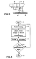
- Figure 5 shows schematically a section of the test apparatus of Figure 4 together with a section of the circuit board, wherein the test head 35 in the maximum remote position to the circuit board 30 (crossed lines) and in a position in which the test needle touches the surface of the circuit board (dashed lines Line) is shown.
- the process begins (step S1) after a printed circuit board, in particular the first printed circuit board of a batch of printed circuit boards to be tested, has been inserted into the test device.
- a positioning movement (S2) is performed, in which the test probe is moved parallel to the plane of the printed circuit board to be tested 30 until the contact tip 7 is arranged approximately at the area of standing on a circuit board test point 36 solder 37. If the test device is not yet calibrated, a corresponding deviation, as shown in FIG. 5 between the solder 37 and the test tip 7, in the position arranged at a distance from the printed circuit board 30, the starting position, results when the positioning movement is actuated.
- the probe is detected again by means of the optical detection device against the background of the printed circuit board 30 to be tested, and the distance and the direction to the center of the printed circuit board test point to be contacted are determined. Thereafter, a correction movement and a movement in the direction of the printed circuit board 30 is again carried out.
- the test probe 7 is now located at a further point P2, which in turn is arranged closer to the solder 37 and to the printed circuit board 30 with respect to the point P1.
- the test probe 7 is detected against the background of the circuit board 30 to be tested, and the distance to the center of the circuit board test point 36 to be contacted is determined.
- test probe moves toward the printed circuit board 30 until the test probe 7 rests on the printed circuit board test point 36.
- the contact of a printed circuit board 30 by means of the test tip 7 or the test needle 4 is detected at the test probe 1 by means of the measuring lug 19 and the light barrier element 18 (FIGS. 1 and 2).
- the vector sum of all correction movements gives the amount and direction of the distance of the contact tip 7 in its initial position from the Lot 37. This distance value is stored. From these calibration data are calculated (S4), which are used in a renewed movement of a test probe to a circuit board test point.
- step S5 it is checked if all selected board test points 36 are tested. If this is not the case, another of the selected board test points 36 is approached with the test probe, which in turn when starting the above correction movements are carried out to hit the board test point safely with the contact tip 7. In turn, calibration data are determined from the corresponding distance values.
- Step S5 determines that all selected board test points have been tested, this means that all calibration data has been determined.
- the procedure for starting the selected board test points can thus be completed (S6). Thereafter, the other circuit board test points or other circuit boards of the batch are tested in the conventional manner.
- the individual board test points are approached automatically, wherein the distance of the probe from the center of the board test point automatically determined based on the captured image that includes the probe and the circuit board test point to be contacted and a corresponding correction movement is performed automatically.
- circuit board test points are contacted correctly even if the position data should not be accurately calibrated or there are deviations in the position of the circuit board test points with respect to their ideal position.
- the reliability of contacting a board test point is significantly increased by the method according to the invention.
- the control device of the test apparatus is designed such that the test probe is moved to a specific location by inputting certain input coordinates.
- these input coordinates are associated with the actual positions of the selected board test points and the calibration data is calculated therefrom.
- both the test device itself is calibrated in one step and with the CAD data to be examined PCB connected.
- the two calibrations explained above are replaced by a single calibration process, which is also carried out during testing of the printed circuit board itself.
- the inventive method for starting up a selected board test point lasts only half to two seconds longer than starting with an already calibrated device, so that the entire testing process compared to testing the calibrated device by about half a minute to three, depending on the number of selected board test points Minutes is delayed. This represents a significant acceleration in testing with finger testers over conventional methods in which the test apparatus must first be calibrated before the actual testing begins.
- the test apparatus may also be expedient for the test apparatus to be calibrated using a first printed circuit board of a batch with a number of, for example, ten to 100 selected board test points, and for the other printed circuit boards to be tested only two to ten selected board test points according to the method according to the invention be so that thereby the position of each circuit board to be tested in the tester is checked.
- offsets, distortions and / or distortions in the board test points layout are determined.
- Such offsets, distortions and / or distortions in the layout of the circuit board test points are in the international patent application WO 02/21893 A2 describes in detail why WO 02/21893 A2 is incorporated in the present patent application with reference.
- the minimum number of board test points to consider is two for each side of the board, as two points specify the layout of the board test points in the test plane. If you want to specify the position of the PCB in three-dimensional space exactly, so at least three PCB test points are to be considered during calibration. However, it may also be convenient to calibrate each board using at least four to ten board test points.
- test probes with integrated optical receiving device requires no additional mechanism for moving a camera, as is the case with conventional finger testers, which calibrate the test device by means of a camera.
- the optical receiving device is in each case arranged on the test probe 1.
- Figure 7 shows an embodiment in which for each side of the receiving area in each case a camera 38 is provided, which is arranged stationarily in the area outside of the trusses 32. With each camera 36, the contact tips 7 of the probes 1 can be detected.
- This structure is mechanically much simpler than the devices described above. However, he needs a very high resolution camera with a good lens, so that the location of the contact tip 7 can be detected with the necessary accuracy of, for example, 0.05 mm.
- the selected board test points must be selected be that when starting the same, the contact tip is not covered by a traverse or other part of the test apparatus relative to the camera 38. Otherwise, the method according to the invention can be carried out in the same way as described above.
Landscapes
- Physics & Mathematics (AREA)
- General Physics & Mathematics (AREA)
- Engineering & Computer Science (AREA)
- General Engineering & Computer Science (AREA)
- Computer Hardware Design (AREA)
- Microelectronics & Electronic Packaging (AREA)
- Tests Of Electronic Circuits (AREA)
- Testing Of Short-Circuits, Discontinuities, Leakage, Or Incorrect Line Connections (AREA)
- Measuring Leads Or Probes (AREA)
Claims (21)
- Dispositif pour tester des cartes à circuits imprimés, comprenant :-- une zone de réception pour recevoir une carte à circuits imprimés à tester (30),-- des doigts de test (1) pour établir en série des contacts avec des points de test de la carte à circuits imprimés (36) d'une carte à circuits imprimés (30) à tester au moyen d'une pointe de contact respective (7), lesdits doigts de test pouvant être déplacés le long de la surface d'une carte à circuits imprimés à tester au moyen d'un dispositif de déplacement (32, 34, 35) et pouvant être abaissés avec leurs pointes de contact vers la carte à circuits imprimés (30),caractérisé par :-- un dispositif de détection optique (2, 21, 26, 38) pour la détection optique de l'une au moins des pointes de contact (7) des doigts de test,-- un système d'évaluation pour capter une image de la pointe de contact et pour déterminer la distance de la pointe de contact (7) au centre d'un point de test (36) de la carte à circuits imprimés avec lequel il s'agit d'établir un contact, et-- un dispositif de commande pour commander le déplacement de la pointe de test (7) en fonction de la mesure de la distance déterminée par le système d'évaluation entre la pointe de test (7) et l'un des points de test (36) de la carte à circuits imprimés qu'il s'agit de tester.
- Dispositif selon la revendication 1,
caractérisé par un système pour déplacer la pointe de contact (7) approximativement perpendiculairement à la surface d'une les cartes à circuits imprimés (30) qu'il s'agit de tester. - Dispositif selon la revendication 2,
caractérisé en ce que le dispositif pour déplacer la pointe de contact (7) approximativement perpendiculairement à la surface d'une carte à circuits imprimés (30) à tester comprend un moteur linéaire. - Dispositif selon l'une des revendications 1 à 3,
caractérisé par des traverses (32), qui surplombent la zone de réception, et sur lesquelles au moins un chariot (34) respectif est agencé avec possibilité de translation, et en ce qu'au moins un doigt de test (1) est agencé sur chaque chariot (34). - Dispositif selon la revendication 4,
caractérisé en ce que les traverses (32) sont déplaçables perpendiculairement à leur extension longitudinale, et/ou les doigts de tests (1) sont réalisés mobiles transversalement à l'extension longitudinale des traverses (32). - Dispositif selon l'une des revendications 1 à 5,
caractérisé en ce que les pointes de contact (7) des doigts de tests sont réalisées chacune sur une sonde de test (1), et en ce que l'une au moins des sondes de test (1) est pourvue d'un dispositif de réception (2) du système de détection optique (3). - Dispositif selon la revendication 6,
caractérisé en ce que le système de réception est une puce de caméra (21). - Dispositif selon la revendication 6,
caractérisé en ce que le système de réception est un câble guide d'ondes lumineuses (26). - Dispositif selon l'une des revendications 1 à 5,
caractérisé en ce que le dispositif de détection optique (3) est agencé stationnaire, et en ce qu'il est réalisé pour la détection optique de l'une au moins des pointes de test (7). - Dispositif selon l'une des revendications 1 à 9,
caractérisé en ce que le dispositif de détection optique (3) comprend une caméra. - Procédé pour tester des cartes à circuits imprimés avec un dispositif destiné à tester des cartes à circuits imprimés, comprenant :-- une zone de réception pour recevoir une carte à circuits imprimés à tester,-- des doigts de test pour établir en série des contacts avec des points de test d'une carte à circuits imprimés à tester au moyen d'une pointe de contact respective, lesdits doigts de test pouvant être déplacés le long de la surface d'une carte à circuits imprimés à tester au moyen d'un dispositif de déplacement et pouvant être posés avec leurs pointes de contact vers la carte à circuits imprimés,-- un dispositif de détection optique pour la détection optique de l'une au moins des pointes de contact des doigts de test, le procédé comprenant les étapes suivantes pour l'approche de points de test choisis sur la carte à circuits imprimés au moyen d'une pointe de contact :-- exécution d'un mouvement de positionnement de l'une des pointes de contact, laquelle est agencée à distance par rapport à la surface d'une carte à circuits imprimés à tester, ladite pointe de contact étant déplacée parallèlement à la surface de la carte à circuits imprimés jusqu'à ce que la pointe de contact soit positionnée approximativement sur une verticale dressée au centre d'un point de test de la carte à circuits imprimés, caractérisé par :-- le déplacement de la pointe de contact perpendiculairement à la surface de la carte à circuits imprimés à tester, en rapprochement de celle-ci, et dans lequel au moyen du dispositif de détection optique, on détecte au moins une fois la position de la pointe de contact par rapport au point de test de la carte à circuits imprimés qu'il s'agit de contacter, et pour exécuter un mouvement de correction dirigé parallèlement à la surface de la carte à circuits imprimés à tester, le dispositif de déplacement est piloté de telle manière que les pointes de contact sont déplacées vers la verticale.
- Procédé selon la revendication 11,
caractérisé en ce que des données de calibrage sont déterminées à partir de la direction et de l'ampleur du mouvement de correction, qui sont prises en compte de lors de mouvements de positionnement ultérieurs. - Procédé selon la revendication 11 ou 12,
caractérisé en ce que le mouvement de correction pour corriger la position d'une pointe de contact est exécuté en plusieurs pas de déplacement, de sorte que la position respective de la pointe de test par rapport au point de test de la carte à circuits imprimés qu'il s'agit de contacter est déterminée entre les pas de déplacement individuels. - Procédé selon la revendication 12 ou 13,
caractérisé en ce que pour chaque lot de cartes à circuits imprimés à tester, on détermine les données de calibrage pour les premières cartes à circuits imprimés du lot à tester, à l'aide de 10 à 100 points de test, et ces données de calibrage sont utilisées pour tester les autres cartes à circuits imprimés du lot. - Procédé selon la revendication 14,
caractérisé en ce que lors du test des autres cartes à circuits imprimés du lot, on détermine des données de calibrage à l'aide d'un certain nombre de points de test, ce nombre étant réduit progressivement entre le test de chaque carte à circuits imprimés. - Procédé selon la revendication 14,
caractérisé en ce que lors du test des autres cartes à circuits imprimés du lot, on détermine des données de calibrage à l'aide de deux à dix points de test. - Procédé selon la revendication 15 ou 16,
caractérisé en ce que lors du test des autres cartes à circuits imprimés du lot, les données de calibrage sont déterminées à l'aide d'un nombre augmenté de points de test s'il se produit une erreur lors de la mise en contact d'un doigt de test avec un point de test sur la carte à circuits imprimés. - Procédé selon l'une des revendications 11 à 17,
caractérisé en ce que l'on utilise un dispositif selon les revendications 1 à 10. - Sonde de test pour un dispositif de test à doigts,
dans lequel la sonde de test est susceptible d'être agencée sur une tête de test (35) qui, pour la mise en contact de points de test, est déplaçable en direction d'une carte à circuits imprimés à tester, et comprend une pointe de contact pour la mise en contact d'un point de test de la carte à circuits imprimés,
caractérisée en ce que la sonde de test (1) comprend un dispositif de détection optique (2) au moyen duquel la pointe de contact (7) peut être détectée de manière optique. - Sonde de test selon la revendication 19,
caractérisée en ce que le dispositif récepteur est une puce de caméra (21). - Sonde de test selon la revendication 19,
caractérisée en ce que le dispositif récepteur est un câble guide d'ondes de lumière (26).
Applications Claiming Priority (3)
| Application Number | Priority Date | Filing Date | Title |
|---|---|---|---|
| DE10220343A DE10220343B4 (de) | 2002-05-07 | 2002-05-07 | Vorrichtung und Verfahren zum Prüfen von Leiterplatten und Prüfsonde |
| DE10220343 | 2002-05-07 | ||
| PCT/EP2003/004468 WO2003096037A1 (fr) | 2002-05-07 | 2003-04-29 | Procede et dispositif pour tester des cartes de circuits imprimes et sonde de test associee |
Publications (2)
| Publication Number | Publication Date |
|---|---|
| EP1502123A1 EP1502123A1 (fr) | 2005-02-02 |
| EP1502123B1 true EP1502123B1 (fr) | 2006-12-06 |
Family
ID=29285168
Family Applications (1)
| Application Number | Title | Priority Date | Filing Date |
|---|---|---|---|
| EP03725115A Expired - Lifetime EP1502123B1 (fr) | 2002-05-07 | 2003-04-29 | Procede et dispositif pour tester des cartes de circuits imprimes et sonde de test associee |
Country Status (10)
| Country | Link |
|---|---|
| US (1) | US7015711B2 (fr) |
| EP (1) | EP1502123B1 (fr) |
| JP (1) | JP4245166B2 (fr) |
| KR (1) | KR100747107B1 (fr) |
| CN (1) | CN100460886C (fr) |
| AT (1) | ATE347700T1 (fr) |
| AU (1) | AU2003227690A1 (fr) |
| DE (2) | DE10220343B4 (fr) |
| TW (1) | TWI239405B (fr) |
| WO (1) | WO2003096037A1 (fr) |
Families Citing this family (123)
| Publication number | Priority date | Publication date | Assignee | Title |
|---|---|---|---|---|
| US6380751B2 (en) | 1992-06-11 | 2002-04-30 | Cascade Microtech, Inc. | Wafer probe station having environment control enclosure |
| US5345170A (en) | 1992-06-11 | 1994-09-06 | Cascade Microtech, Inc. | Wafer probe station having integrated guarding, Kelvin connection and shielding systems |
| US5561377A (en) | 1995-04-14 | 1996-10-01 | Cascade Microtech, Inc. | System for evaluating probing networks |
| US6232789B1 (en) * | 1997-05-28 | 2001-05-15 | Cascade Microtech, Inc. | Probe holder for low current measurements |
| US5729150A (en) * | 1995-12-01 | 1998-03-17 | Cascade Microtech, Inc. | Low-current probe card with reduced triboelectric current generating cables |
| US5914613A (en) * | 1996-08-08 | 1999-06-22 | Cascade Microtech, Inc. | Membrane probing system with local contact scrub |
| US6002263A (en) | 1997-06-06 | 1999-12-14 | Cascade Microtech, Inc. | Probe station having inner and outer shielding |
| US6034533A (en) * | 1997-06-10 | 2000-03-07 | Tervo; Paul A. | Low-current pogo probe card |
| US6256882B1 (en) | 1998-07-14 | 2001-07-10 | Cascade Microtech, Inc. | Membrane probing system |
| US6578264B1 (en) * | 1999-06-04 | 2003-06-17 | Cascade Microtech, Inc. | Method for constructing a membrane probe using a depression |
| US6445202B1 (en) | 1999-06-30 | 2002-09-03 | Cascade Microtech, Inc. | Probe station thermal chuck with shielding for capacitive current |
| US6838890B2 (en) * | 2000-02-25 | 2005-01-04 | Cascade Microtech, Inc. | Membrane probing system |
| US6914423B2 (en) | 2000-09-05 | 2005-07-05 | Cascade Microtech, Inc. | Probe station |
| US6965226B2 (en) | 2000-09-05 | 2005-11-15 | Cascade Microtech, Inc. | Chuck for holding a device under test |
| DE10143173A1 (de) | 2000-12-04 | 2002-06-06 | Cascade Microtech Inc | Wafersonde |
| WO2003052435A1 (fr) * | 2001-08-21 | 2003-06-26 | Cascade Microtech, Inc. | Systeme de detection a membrane |
| WO2003020467A1 (fr) | 2001-08-31 | 2003-03-13 | Cascade Microtech, Inc. | Appareil de test optique |
| US6777964B2 (en) | 2002-01-25 | 2004-08-17 | Cascade Microtech, Inc. | Probe station |
| US6951846B2 (en) * | 2002-03-07 | 2005-10-04 | The United States Of America As Represented By The Secretary Of The Army | Artemisinins with improved stability and bioavailability for therapeutic drug development and application |
| JP2005527823A (ja) | 2002-05-23 | 2005-09-15 | カスケード マイクロテック インコーポレイテッド | デバイスのテスト用プローブ |
| US6847219B1 (en) | 2002-11-08 | 2005-01-25 | Cascade Microtech, Inc. | Probe station with low noise characteristics |
| US6724205B1 (en) | 2002-11-13 | 2004-04-20 | Cascade Microtech, Inc. | Probe for combined signals |
| US7250779B2 (en) | 2002-11-25 | 2007-07-31 | Cascade Microtech, Inc. | Probe station with low inductance path |
| US6861856B2 (en) | 2002-12-13 | 2005-03-01 | Cascade Microtech, Inc. | Guarded tub enclosure |
| DE10320381B4 (de) * | 2003-05-06 | 2010-11-04 | Scorpion Technologies Ag | Platinentestvorrichtung mit schrägstehend angetriebenen Kontaktiernadeln |
| US7221172B2 (en) | 2003-05-06 | 2007-05-22 | Cascade Microtech, Inc. | Switched suspended conductor and connection |
| DE10320925B4 (de) * | 2003-05-09 | 2007-07-05 | Atg Test Systems Gmbh & Co.Kg | Verfahren zum Testen von unbestückten Leiterplatten |
| US7492172B2 (en) | 2003-05-23 | 2009-02-17 | Cascade Microtech, Inc. | Chuck for holding a device under test |
| US7057404B2 (en) | 2003-05-23 | 2006-06-06 | Sharp Laboratories Of America, Inc. | Shielded probe for testing a device under test |
| US7250626B2 (en) | 2003-10-22 | 2007-07-31 | Cascade Microtech, Inc. | Probe testing structure |
| DE202004021093U1 (de) | 2003-12-24 | 2006-09-28 | Cascade Microtech, Inc., Beaverton | Aktiver Halbleiterscheibenmessfühler |
| US7187188B2 (en) | 2003-12-24 | 2007-03-06 | Cascade Microtech, Inc. | Chuck with integrated wafer support |
| US7518391B2 (en) * | 2004-02-17 | 2009-04-14 | Applied Materials, Israel, Ltd. | Probe card and a method for detecting defects using a probe card and an additional inspection |
| TW200537110A (en) * | 2004-05-14 | 2005-11-16 | Innolux Display Corp | Testing apparatus |
| JP2008502167A (ja) | 2004-06-07 | 2008-01-24 | カスケード マイクロテック インコーポレイテッド | 熱光学チャック |
| US7330041B2 (en) | 2004-06-14 | 2008-02-12 | Cascade Microtech, Inc. | Localizing a temperature of a device for testing |
| KR100591667B1 (ko) * | 2004-06-22 | 2006-06-19 | (주)알티에스 | 반도체 칩 측정 장치 및 측정 방법 |
| US7368927B2 (en) | 2004-07-07 | 2008-05-06 | Cascade Microtech, Inc. | Probe head having a membrane suspended probe |
| KR20070058522A (ko) | 2004-09-13 | 2007-06-08 | 캐스케이드 마이크로테크 인코포레이티드 | 양측 프루빙 구조 |
| US7535247B2 (en) | 2005-01-31 | 2009-05-19 | Cascade Microtech, Inc. | Interface for testing semiconductors |
| US7656172B2 (en) | 2005-01-31 | 2010-02-02 | Cascade Microtech, Inc. | System for testing semiconductors |
| US7449899B2 (en) | 2005-06-08 | 2008-11-11 | Cascade Microtech, Inc. | Probe for high frequency signals |
| US20070294047A1 (en) * | 2005-06-11 | 2007-12-20 | Leonard Hayden | Calibration system |
| JP5080459B2 (ja) | 2005-06-13 | 2012-11-21 | カスケード マイクロテック インコーポレイテッド | 広帯域能動/受動差動信号プローブ |
| US7463042B2 (en) * | 2005-06-30 | 2008-12-09 | Northrop Grumman Corporation | Connector probing system |
| EP1739440A3 (fr) * | 2005-06-30 | 2009-05-13 | Feinmetall GmbH | Procédé et appareil pour test éléctrique et procédé de fabrication d'un dispositif de contact |
| KR100696864B1 (ko) * | 2005-09-26 | 2007-03-20 | 삼성전자주식회사 | 기판 검사 방법 및 이를 수행하기 위한 장치 |
| DE102006005800B4 (de) * | 2006-02-08 | 2007-12-06 | Atg Test Systems Gmbh | Verfahren und Vorrichtung zum Testen von unbestückten Leiterplatten |
| DE102006006255A1 (de) * | 2006-02-10 | 2007-08-23 | Atg Test Systems Gmbh | Fingertester zum Prüfen von unbestückten Leiterplatten und Verfahren zum Prüfen unbestückter Leiterplatten mit einem Fingertester |
| DE202007018733U1 (de) | 2006-06-09 | 2009-03-26 | Cascade Microtech, Inc., Beaverton | Messfühler für differentielle Signale mit integrierter Symmetrieschaltung |
| US7403028B2 (en) | 2006-06-12 | 2008-07-22 | Cascade Microtech, Inc. | Test structure and probe for differential signals |
| US7764072B2 (en) | 2006-06-12 | 2010-07-27 | Cascade Microtech, Inc. | Differential signal probing system |
| US7443186B2 (en) | 2006-06-12 | 2008-10-28 | Cascade Microtech, Inc. | On-wafer test structures for differential signals |
| US7723999B2 (en) | 2006-06-12 | 2010-05-25 | Cascade Microtech, Inc. | Calibration structures for differential signal probing |
| DE202006020417U1 (de) | 2006-07-28 | 2008-07-10 | Ptr Messtechnik Gmbh & Co. Kg | Schaltfederkontaktstift |
| US8436636B2 (en) * | 2006-10-10 | 2013-05-07 | Apple Inc. | Methods and apparatuses for testing circuit boards |
| JP4461159B2 (ja) * | 2007-06-14 | 2010-05-12 | ヤマハファインテック株式会社 | プリント基板の検査装置および検査方法 |
| JP4539685B2 (ja) * | 2007-06-22 | 2010-09-08 | セイコーエプソン株式会社 | 部品搬送装置及びicハンドラ |
| US7876114B2 (en) | 2007-08-08 | 2011-01-25 | Cascade Microtech, Inc. | Differential waveguide probe |
| KR100788640B1 (ko) * | 2007-08-09 | 2007-12-26 | 주식회사 파이컴 | 기판 모듈, 기판 어셈블리 그리고 이를 포함하는 전기 검사장치 |
| US20090045826A1 (en) * | 2007-08-18 | 2009-02-19 | Samo Sustarsic | Measuring probe with optical cable |
| US7724007B2 (en) * | 2007-09-28 | 2010-05-25 | Tokyo Electron Limited | Probe apparatus and probing method |
| TW200918914A (en) * | 2007-10-24 | 2009-05-01 | King Yuan Electronics Co Ltd | Testing system module |
| US8008938B2 (en) * | 2007-10-24 | 2011-08-30 | King Yuan Electronics Co., Ltd. | Testing system module |
| JP5088167B2 (ja) * | 2008-02-22 | 2012-12-05 | 東京エレクトロン株式会社 | プローブ装置、プロービング方法及び記憶媒体 |
| US7595628B1 (en) * | 2008-06-04 | 2009-09-29 | Lecroy Corporation | Probing apparatus for illuminating an electrical device under test |
| US7847575B2 (en) * | 2008-07-28 | 2010-12-07 | Globalfoundries Inc. | Method and apparatus for nano probing a semiconductor chip |
| US7888957B2 (en) | 2008-10-06 | 2011-02-15 | Cascade Microtech, Inc. | Probing apparatus with impedance optimized interface |
| US8253784B2 (en) * | 2008-11-13 | 2012-08-28 | Honeywell International Inc. | Image capturing device assembly for use with test probe |
| WO2010059247A2 (fr) | 2008-11-21 | 2010-05-27 | Cascade Microtech, Inc. | Coupon amovible pour appareil de sondage |
| US8319503B2 (en) | 2008-11-24 | 2012-11-27 | Cascade Microtech, Inc. | Test apparatus for measuring a characteristic of a device under test |
| TWI412754B (zh) * | 2009-05-15 | 2013-10-21 | Hon Hai Prec Ind Co Ltd | 特性阻抗測試系統及方法 |
| DE102010023187A1 (de) | 2010-06-09 | 2011-12-15 | Dtg International Gmbh | Vorrichtung und Verfahren zum Untersuchen von Leiterplatten |
| TWI410644B (zh) * | 2010-08-13 | 2013-10-01 | Gemtek Technology Co Ltd | 量測系統 |
| US9658252B2 (en) * | 2011-02-21 | 2017-05-23 | United Microelectronics Corp. | Probe insertion auxiliary and method of probe insertion |
| CN102785252A (zh) * | 2011-05-19 | 2012-11-21 | 鸿富锦精密工业(深圳)有限公司 | 机械手及检测装置 |
| WO2012163064A1 (fr) | 2011-06-01 | 2012-12-06 | 浙江省电力公司 | Système et procédé de détection entièrement automatique pour transformateur |
| CN102323560A (zh) * | 2011-06-01 | 2012-01-18 | 浙江省电力公司 | 一种互感器在线检测用工装板 |
| JP6088145B2 (ja) * | 2012-02-13 | 2017-03-01 | オートモーティブエナジーサプライ株式会社 | 電池の製造方法および導電性検査装置 |
| WO2014009542A2 (fr) * | 2012-07-12 | 2014-01-16 | Konrad Gmbh | Dispositif pour produire et/ou usiner une pièce |
| KR101354729B1 (ko) * | 2012-08-23 | 2014-01-27 | 앰코 테크놀로지 코리아 주식회사 | 반도체 디바이스의 오정렬 값 측정 방법 및 이것이 적용된 반도체 디바이스 |
| WO2014079913A1 (fr) * | 2012-11-21 | 2014-05-30 | Konrad Gmbh | Procédé et dispositif de contrôle d'une pièce |
| DE102013102564A1 (de) * | 2013-03-13 | 2014-09-18 | Dtg International Gmbh | Traverseneinheit für eine Prüfvorrichtung für Leiterplatten, sowie Prüfvorrichtung damit |
| US9989583B2 (en) | 2013-03-13 | 2018-06-05 | Xcerra Corporation | Cross-bar unit for a test apparatus for circuit boards, and test apparatus containing the former |
| KR102026357B1 (ko) * | 2013-04-17 | 2019-11-04 | (주)테크윙 | 반도체소자 테스트용 핸들러 |
| CN103344905B (zh) * | 2013-06-18 | 2016-02-10 | 大族激光科技产业集团股份有限公司 | 运动针床测试机及测试方法 |
| CN105021938B (zh) * | 2014-04-30 | 2018-11-09 | 佰欧特株式会社 | 检查装置 |
| CN105572450B (zh) * | 2014-10-17 | 2018-12-14 | 群光电能科技股份有限公司 | 电源供应器测量设备及其测量方法 |
| US9506961B2 (en) * | 2014-12-04 | 2016-11-29 | Chicony Power Technology Co., Ltd. | Power supply detection apparatus and detecting method thereof |
| DE102015113046A1 (de) * | 2015-08-07 | 2017-02-09 | Xcerra Corp. | Positioniereinrichtung für einen Paralleltester zum Testen von Leiterplatten und Paralleltester zum Testen von Leiterplatten |
| CN105158675A (zh) * | 2015-09-09 | 2015-12-16 | 重庆川仪自动化股份有限公司 | 电路板测试的方法及系统 |
| TWI586967B (zh) * | 2015-10-27 | 2017-06-11 | Mpi Corp | Probe module |
| DE202016008239U1 (de) * | 2015-11-09 | 2017-06-12 | Feinmetall Gmbh | Kontaktstift mit Lichtquelle und Kontaktstiftanordnung mit Lichtquelle |
| CN105407703B (zh) * | 2015-12-17 | 2018-11-13 | 埃泰克汽车电子(芜湖)有限公司 | 用于pcb半成品的测试装置及其测试方法 |
| JP2018031597A (ja) * | 2016-08-22 | 2018-03-01 | Koa株式会社 | プローブユニット |
| US10459006B2 (en) * | 2016-09-28 | 2019-10-29 | Formfactor Beaverton, Inc. | Probe systems and methods |
| US10371718B2 (en) | 2016-11-14 | 2019-08-06 | International Business Machines Corporation | Method for identification of proper probe placement on printed circuit board |
| DE102017102700A1 (de) | 2017-02-10 | 2018-09-13 | Atg Luther & Maelzer Gmbh | Prüfvorrichtung und Verfahren zum Prüfen von Leiterplatten |
| CN108253734B (zh) * | 2017-10-20 | 2024-03-12 | 中山凯旋真空科技股份有限公司 | 用于真空干燥罐的拉绳安全装置及真空干燥罐 |
| EP4471435A3 (fr) | 2018-01-18 | 2025-03-05 | atg Luther & Maelzer GmbH | Aiguille de test, sonde de test et testeur à doigt pour tester les circuits imprimés |
| CN108414920A (zh) * | 2018-03-15 | 2018-08-17 | 昆山翰辉电子科技有限公司 | 线路板测试设备 |
| KR102025537B1 (ko) * | 2018-06-25 | 2019-09-26 | (주)티에스이 | 반도체 패키지 검사장치 |
| KR101981653B1 (ko) * | 2018-06-29 | 2019-05-24 | 한국알프스 주식회사 | 기판 테스트 장비 |
| JP7134566B2 (ja) * | 2018-09-10 | 2022-09-12 | 株式会社ディスコ | チップ破壊ユニット、チップの強度の比較方法 |
| US11125780B2 (en) * | 2018-10-18 | 2021-09-21 | International Business Machines Corporation | Test probe assembly with fiber optic leads and photodetectors |
| US11119148B2 (en) * | 2018-10-18 | 2021-09-14 | International Business Machines Corporation | Test probe assembly with fiber optic leads and photodetectors for testing semiconductor wafers |
| CN111258825B (zh) * | 2018-11-30 | 2023-11-14 | 上海海拉电子有限公司 | 一种用于电路板中测试点布置的装置及方法 |
| EP3686610B1 (fr) | 2019-01-24 | 2025-03-05 | Rohde & Schwarz GmbH & Co. KG | Sonde, système de mesure et procédé d'application d'une sonde |
| JP7227067B2 (ja) * | 2019-05-08 | 2023-02-21 | 株式会社日本マイクロニクス | 検査用接続装置 |
| US11204383B2 (en) * | 2019-09-30 | 2021-12-21 | Formfactor, Inc. | Methods for maintaining gap spacing between an optical probe of a probe system and an optical device of a device under test, and probe systems that perform the methods |
| US11131709B2 (en) | 2019-09-30 | 2021-09-28 | Formfactor, Inc. | Probe systems for optically probing a device under test and methods of operating the probe systems |
| TWI712802B (zh) * | 2020-01-21 | 2020-12-11 | 中華精測科技股份有限公司 | 探針卡裝置及其類頸式探針 |
| KR102405296B1 (ko) * | 2020-05-19 | 2022-06-07 | 주식회사 에머릭스 | 기판 검사 장치 |
| WO2023276002A1 (fr) * | 2021-06-29 | 2023-01-05 | 株式会社日立ハイテク | Dispositif de sonde |
| US12236176B2 (en) | 2021-10-13 | 2025-02-25 | Albert Moses Haim | System and method for trace generation and reconfiguration on a breadboard or printed circuit board |
| US11363713B1 (en) | 2021-10-13 | 2022-06-14 | Albert Moses Haim | System and method for trace generation and reconfiguration on a breadboard or printed circuit board |
| CN114076888A (zh) * | 2021-11-17 | 2022-02-22 | 北京芯同汇科技有限公司 | 电路板辐射场频谱分量测量装置及电路板运行检测方法 |
| CN114441942B (zh) * | 2022-01-28 | 2023-10-03 | 苏州格拉尼视觉科技有限公司 | Pcb板的飞针测试方法、系统、设备及存储介质 |
| CN114942381A (zh) * | 2022-07-21 | 2022-08-26 | 深圳市东方宇之光科技股份有限公司 | 基于悬臂式结构测试电路板的飞针测试机及测试方法 |
| KR102534507B1 (ko) | 2022-12-23 | 2023-05-18 | 김응호 | 회로 기판 검사 시스템 |
| TWI891316B (zh) * | 2024-04-03 | 2025-07-21 | 鴻勁精密股份有限公司 | 測試裝置及作業機 |
| KR102912225B1 (ko) * | 2024-11-21 | 2026-01-16 | 한국철도기술연구원 | 회로의 고주파 패턴 측정용 rf 프로브 장치 |
| CN119716495B (zh) * | 2025-02-27 | 2025-06-13 | 常州固堡电子有限公司 | 一种柔性线路板检测装置 |
Family Cites Families (22)
| Publication number | Priority date | Publication date | Assignee | Title |
|---|---|---|---|---|
| JPS60263807A (ja) * | 1984-06-12 | 1985-12-27 | Dainippon Screen Mfg Co Ltd | プリント配線板のパタ−ン欠陥検査装置 |
| JPS6115341A (ja) * | 1984-07-02 | 1986-01-23 | Canon Inc | ウエハプロ−バ |
| GB8700754D0 (en) * | 1987-01-14 | 1987-02-18 | Int Computers Ltd | Test apparatus for printed circuit boards |
| US4929893A (en) * | 1987-10-06 | 1990-05-29 | Canon Kabushiki Kaisha | Wafer prober |
| JPH03209737A (ja) * | 1990-01-11 | 1991-09-12 | Tokyo Electron Ltd | プローブ装置 |
| DE4109684C2 (de) * | 1990-07-25 | 2001-07-12 | Atg Test Systems Gmbh | Kontaktierungsvorrichtung für Prüfzwecke |
| EP0468153B1 (fr) * | 1990-07-25 | 1995-10-11 | atg test systems GmbH | Dispositif pour contacter des éléments à tester |
| US5113133A (en) * | 1990-12-20 | 1992-05-12 | Integri-Test Corporation | Circuit board test probe |
| WO1992011541A1 (fr) * | 1990-12-21 | 1992-07-09 | Huntron Instruments, Inc. | Systeme d'acquisition d'images utilise avec un appareil de verification de plaquettes de circuits imprimes |
| JPH05196681A (ja) * | 1991-06-26 | 1993-08-06 | Digital Equip Corp <Dec> | 連続移動する電気回路の相互接続試験方法及び装置 |
| US5394100A (en) * | 1993-05-06 | 1995-02-28 | Karl Suss America, Incorporated | Probe system with automatic control of contact pressure and probe alignment |
| US5644245A (en) * | 1993-11-24 | 1997-07-01 | Tokyo Electron Limited | Probe apparatus for inspecting electrical characteristics of a microelectronic element |
| US5804982A (en) * | 1995-05-26 | 1998-09-08 | International Business Machines Corporation | Miniature probe positioning actuator |
| DE19700505A1 (de) * | 1997-01-09 | 1998-07-16 | Atg Test Systems Gmbh | Verfahren zum Prüfen von Leiterplatten |
| US6356093B2 (en) * | 1998-06-02 | 2002-03-12 | Nidec-Read Corporation | Printed circuit board testing apparatus |
| DE19844428B4 (de) * | 1998-09-28 | 2004-05-13 | Atg Test Systems Gmbh & Co.Kg | Prüfsonde für einen Fingertester, ein Verfahren zum Ansteuern einer Prüfsonde, Fingertester zum Prüfen von Leiterplatten und ein Verfahren zum Prüfen von Leiterplatten mit einem Fingertester |
| US6496361B2 (en) * | 1998-11-16 | 2002-12-17 | Acer Incorporated | Embedded CMOS camera in a laptop computer |
| US6734687B1 (en) * | 2000-02-25 | 2004-05-11 | Hitachi, Ltd. | Apparatus for detecting defect in device and method of detecting defect |
| DE20005123U1 (de) * | 2000-03-20 | 2001-08-02 | atg test systems GmbH & Co. KG Reicholzheim, 97877 Wertheim | Vorrichtung zum Prüfen von Leiterplatten |
| JP4408538B2 (ja) * | 2000-07-24 | 2010-02-03 | 株式会社日立製作所 | プローブ装置 |
| DE10043728C2 (de) * | 2000-09-05 | 2003-12-04 | Atg Test Systems Gmbh | Verfahren zum Prüfen von Leiterplatten und Verwendung einer Vorrichtung zum Ausführen des Verfahrens |
| DE10160119A1 (de) * | 2001-12-07 | 2003-10-02 | Atg Test Systems Gmbh | Prüfsonde für einen Fingertester |
-
2002
- 2002-05-07 DE DE10220343A patent/DE10220343B4/de not_active Expired - Fee Related
-
2003
- 2003-04-29 JP JP2004503977A patent/JP4245166B2/ja not_active Expired - Fee Related
- 2003-04-29 CN CNB038101149A patent/CN100460886C/zh not_active Expired - Fee Related
- 2003-04-29 AT AT03725115T patent/ATE347700T1/de not_active IP Right Cessation
- 2003-04-29 DE DE50305905T patent/DE50305905D1/de not_active Expired - Lifetime
- 2003-04-29 KR KR1020047017748A patent/KR100747107B1/ko not_active Expired - Fee Related
- 2003-04-29 EP EP03725115A patent/EP1502123B1/fr not_active Expired - Lifetime
- 2003-04-29 AU AU2003227690A patent/AU2003227690A1/en not_active Abandoned
- 2003-04-29 WO PCT/EP2003/004468 patent/WO2003096037A1/fr not_active Ceased
- 2003-05-05 TW TW092112245A patent/TWI239405B/zh not_active IP Right Cessation
-
2004
- 2004-11-04 US US10/981,079 patent/US7015711B2/en not_active Expired - Fee Related
Also Published As
| Publication number | Publication date |
|---|---|
| KR100747107B1 (ko) | 2007-08-07 |
| TW200400360A (en) | 2004-01-01 |
| AU2003227690A1 (en) | 2003-11-11 |
| EP1502123A1 (fr) | 2005-02-02 |
| KR20050003407A (ko) | 2005-01-10 |
| CN100460886C (zh) | 2009-02-11 |
| ATE347700T1 (de) | 2006-12-15 |
| JP4245166B2 (ja) | 2009-03-25 |
| DE50305905D1 (de) | 2007-01-18 |
| JP2005532535A (ja) | 2005-10-27 |
| CN1650181A (zh) | 2005-08-03 |
| US20050083038A1 (en) | 2005-04-21 |
| US7015711B2 (en) | 2006-03-21 |
| DE10220343A1 (de) | 2003-11-27 |
| TWI239405B (en) | 2005-09-11 |
| WO2003096037A1 (fr) | 2003-11-20 |
| DE10220343B4 (de) | 2007-04-05 |
Similar Documents
| Publication | Publication Date | Title |
|---|---|---|
| EP1502123B1 (fr) | Procede et dispositif pour tester des cartes de circuits imprimes et sonde de test associee | |
| EP1982203B1 (fr) | Procédé et dispositif pour tester des cartes de circuits imprimés nus | |
| DE68908752T2 (de) | Ausgleichsanordnung zur Untersuchung von möglicherweise gekrümmten Leiterplatten. | |
| EP1285408B1 (fr) | Procede et dispositif pour examiner une zone predeterminee d'un circuit imprime | |
| DE4417580C2 (de) | Testvorrichtung zum Testen einer elektronischen Schaltungsplatine | |
| EP1623242B1 (fr) | Procédé pour tester des cartes des circuits imprimées non-équipées | |
| EP1186898B1 (fr) | Procédé et appareil pour tester des circuits imprimés | |
| DE102004058483B4 (de) | Vorrichtung zur Untersuchung von Produkten auf Fehler, Messfühler-Positionierverfahren und Messfühler-Bewegungsverfahren | |
| WO2010081834A1 (fr) | Procédé d'essai de plaquettes à circuit imprimé | |
| DE10039928B4 (de) | Vorrichtung zum automatisierten Testen, Kalibrieren und Charakterisieren von Testadaptern | |
| EP3740767A1 (fr) | Aiguille de test capacitif pour mesurer des couches électriquement conductrices dans des trous de carte de circuit imprimé | |
| EP0853242A1 (fr) | Procédé pour tester des cartes de circuits imprimés | |
| EP1315975B1 (fr) | Procede et dispositif pour tester des cartes de circuits imprimes au moyen d'un testeur en parallele | |
| EP1982197B1 (fr) | Testeur à pattes pour contrôler des cartes de circuits imprimés non équipées et procédé de contrôle de cartes de circuits imprimés non équipées avec un testeur à pattes | |
| DE19847913A1 (de) | Vorrichtung und Verfahren zur optischen Inspektion insbesondere verdeckter Lötverbindungen | |
| EP1920263B1 (fr) | Procede pour tester des cartes de circuits imprimes de grandes surfaces non equipees, au moyen d'un testeur a pattes | |
| EP1739440A2 (fr) | Procédé et appareil pour test éléctrique et procédé de fabrication d'un dispositif de contact | |
| DE102024121480A1 (de) | Verfahren zur Bestimmung von Sondierungsparametern für ein Sondensystem zur Prüfung einer Vorrichtung unter Test, Sondensystem und Verfahren zum Betrieb desselben, nicht-transitorische Computer-lesbare Speichermedien, Verfahren zur Prüfung einer unverpackten Halbleitervorrichtung, geprüfte Halbleitervorrichtung und Verfahren zur Herstellung derselben, und Verfahren zur Erzeugung eines virtuellen Markierungsbildes | |
| EP0864874A2 (fr) | Procédé et dispositif de contrÔle de cartes de circuit | |
| DE3728818A1 (de) | Anordnung zum ermitteln und beseitigen von fertigungsfehlern einer elektrischen baugruppe | |
| WO1999008499A1 (fr) | Procede et dispositif pour identifier la position et/ou controler la coplanarite et/ou controler la separation de connexions de composants | |
| DE102004036819A1 (de) | Verfahren zur Bestimmung der Bestückgenauigkeit eines Bestückautomaten, optisches Messsystem | |
| DE102004045742B3 (de) | Verfahren zur Bestimmung der relativen räumlichen Lage zwischen zwei Kameras, Vorrichtung zum Bestücken von Bauelementeträgern | |
| WO2001040809A1 (fr) | Procede et dispositif pour tester des cartes de circuits | |
| AT502410A4 (de) | Vorrichtung zur prüfung von werkstücken |
Legal Events
| Date | Code | Title | Description |
|---|---|---|---|
| PUAI | Public reference made under article 153(3) epc to a published international application that has entered the european phase |
Free format text: ORIGINAL CODE: 0009012 |
|
| 17P | Request for examination filed |
Effective date: 20041029 |
|
| AK | Designated contracting states |
Kind code of ref document: A1 Designated state(s): AT BE BG CH CY CZ DE DK EE ES FI FR GB GR HU IE IT LI LU MC NL PT RO SE SI SK TR |
|
| AX | Request for extension of the european patent |
Extension state: AL LT LV MK |
|
| DAX | Request for extension of the european patent (deleted) | ||
| GRAP | Despatch of communication of intention to grant a patent |
Free format text: ORIGINAL CODE: EPIDOSNIGR1 |
|
| GRAS | Grant fee paid |
Free format text: ORIGINAL CODE: EPIDOSNIGR3 |
|
| GRAA | (expected) grant |
Free format text: ORIGINAL CODE: 0009210 |
|
| RAP1 | Party data changed (applicant data changed or rights of an application transferred) |
Owner name: ATG TEST SYSTEMS GMBH |
|
| AK | Designated contracting states |
Kind code of ref document: B1 Designated state(s): AT BE BG CH CY CZ DE DK EE ES FI FR GB GR HU IE IT LI LU MC NL PT RO SE SI SK TR |
|
| PG25 | Lapsed in a contracting state [announced via postgrant information from national office to epo] |
Ref country code: IE Free format text: LAPSE BECAUSE OF FAILURE TO SUBMIT A TRANSLATION OF THE DESCRIPTION OR TO PAY THE FEE WITHIN THE PRESCRIBED TIME-LIMIT Effective date: 20061206 Ref country code: DK Free format text: LAPSE BECAUSE OF FAILURE TO SUBMIT A TRANSLATION OF THE DESCRIPTION OR TO PAY THE FEE WITHIN THE PRESCRIBED TIME-LIMIT Effective date: 20061206 Ref country code: RO Free format text: LAPSE BECAUSE OF FAILURE TO SUBMIT A TRANSLATION OF THE DESCRIPTION OR TO PAY THE FEE WITHIN THE PRESCRIBED TIME-LIMIT Effective date: 20061206 Ref country code: NL Free format text: LAPSE BECAUSE OF FAILURE TO SUBMIT A TRANSLATION OF THE DESCRIPTION OR TO PAY THE FEE WITHIN THE PRESCRIBED TIME-LIMIT Effective date: 20061206 Ref country code: CZ Free format text: LAPSE BECAUSE OF FAILURE TO SUBMIT A TRANSLATION OF THE DESCRIPTION OR TO PAY THE FEE WITHIN THE PRESCRIBED TIME-LIMIT Effective date: 20061206 Ref country code: SI Free format text: LAPSE BECAUSE OF FAILURE TO SUBMIT A TRANSLATION OF THE DESCRIPTION OR TO PAY THE FEE WITHIN THE PRESCRIBED TIME-LIMIT Effective date: 20061206 Ref country code: SK Free format text: LAPSE BECAUSE OF FAILURE TO SUBMIT A TRANSLATION OF THE DESCRIPTION OR TO PAY THE FEE WITHIN THE PRESCRIBED TIME-LIMIT Effective date: 20061206 |
|
| REG | Reference to a national code |
Ref country code: GB Ref legal event code: FG4D Free format text: NOT ENGLISH |
|
| REG | Reference to a national code |
Ref country code: CH Ref legal event code: EP |
|
| REG | Reference to a national code |
Ref country code: IE Ref legal event code: FG4D Free format text: LANGUAGE OF EP DOCUMENT: GERMAN |
|
| REF | Corresponds to: |
Ref document number: 50305905 Country of ref document: DE Date of ref document: 20070118 Kind code of ref document: P |
|
| PG25 | Lapsed in a contracting state [announced via postgrant information from national office to epo] |
Ref country code: BG Free format text: LAPSE BECAUSE OF FAILURE TO SUBMIT A TRANSLATION OF THE DESCRIPTION OR TO PAY THE FEE WITHIN THE PRESCRIBED TIME-LIMIT Effective date: 20070306 Ref country code: SE Free format text: LAPSE BECAUSE OF FAILURE TO SUBMIT A TRANSLATION OF THE DESCRIPTION OR TO PAY THE FEE WITHIN THE PRESCRIBED TIME-LIMIT Effective date: 20070306 |
|
| PG25 | Lapsed in a contracting state [announced via postgrant information from national office to epo] |
Ref country code: ES Free format text: LAPSE BECAUSE OF FAILURE TO SUBMIT A TRANSLATION OF THE DESCRIPTION OR TO PAY THE FEE WITHIN THE PRESCRIBED TIME-LIMIT Effective date: 20070317 |
|
| PG25 | Lapsed in a contracting state [announced via postgrant information from national office to epo] |
Ref country code: PT Free format text: LAPSE BECAUSE OF FAILURE TO SUBMIT A TRANSLATION OF THE DESCRIPTION OR TO PAY THE FEE WITHIN THE PRESCRIBED TIME-LIMIT Effective date: 20070507 |
|
| NLV1 | Nl: lapsed or annulled due to failure to fulfill the requirements of art. 29p and 29m of the patents act | ||
| ET | Fr: translation filed | ||
| PLBE | No opposition filed within time limit |
Free format text: ORIGINAL CODE: 0009261 |
|
| STAA | Information on the status of an ep patent application or granted ep patent |
Free format text: STATUS: NO OPPOSITION FILED WITHIN TIME LIMIT |
|
| 26N | No opposition filed |
Effective date: 20070907 |
|
| REG | Reference to a national code |
Ref country code: CH Ref legal event code: PL |
|
| BERE | Be: lapsed |
Owner name: ATG TEST SYSTEMS G.M.B.H. Effective date: 20070430 |
|
| PG25 | Lapsed in a contracting state [announced via postgrant information from national office to epo] |
Ref country code: LI Free format text: LAPSE BECAUSE OF NON-PAYMENT OF DUE FEES Effective date: 20070430 Ref country code: CH Free format text: LAPSE BECAUSE OF NON-PAYMENT OF DUE FEES Effective date: 20070430 |
|
| PG25 | Lapsed in a contracting state [announced via postgrant information from national office to epo] |
Ref country code: BE Free format text: LAPSE BECAUSE OF NON-PAYMENT OF DUE FEES Effective date: 20070430 |
|
| PG25 | Lapsed in a contracting state [announced via postgrant information from national office to epo] |
Ref country code: GR Free format text: LAPSE BECAUSE OF FAILURE TO SUBMIT A TRANSLATION OF THE DESCRIPTION OR TO PAY THE FEE WITHIN THE PRESCRIBED TIME-LIMIT Effective date: 20070307 |
|
| PG25 | Lapsed in a contracting state [announced via postgrant information from national office to epo] |
Ref country code: AT Free format text: LAPSE BECAUSE OF NON-PAYMENT OF DUE FEES Effective date: 20070429 |
|
| PG25 | Lapsed in a contracting state [announced via postgrant information from national office to epo] |
Ref country code: EE Free format text: LAPSE BECAUSE OF FAILURE TO SUBMIT A TRANSLATION OF THE DESCRIPTION OR TO PAY THE FEE WITHIN THE PRESCRIBED TIME-LIMIT Effective date: 20061206 |
|
| PG25 | Lapsed in a contracting state [announced via postgrant information from national office to epo] |
Ref country code: MC Free format text: LAPSE BECAUSE OF NON-PAYMENT OF DUE FEES Effective date: 20070430 |
|
| PG25 | Lapsed in a contracting state [announced via postgrant information from national office to epo] |
Ref country code: LU Free format text: LAPSE BECAUSE OF NON-PAYMENT OF DUE FEES Effective date: 20070429 Ref country code: CY Free format text: LAPSE BECAUSE OF FAILURE TO SUBMIT A TRANSLATION OF THE DESCRIPTION OR TO PAY THE FEE WITHIN THE PRESCRIBED TIME-LIMIT Effective date: 20061206 |
|
| PG25 | Lapsed in a contracting state [announced via postgrant information from national office to epo] |
Ref country code: TR Free format text: LAPSE BECAUSE OF FAILURE TO SUBMIT A TRANSLATION OF THE DESCRIPTION OR TO PAY THE FEE WITHIN THE PRESCRIBED TIME-LIMIT Effective date: 20061206 Ref country code: HU Free format text: LAPSE BECAUSE OF FAILURE TO SUBMIT A TRANSLATION OF THE DESCRIPTION OR TO PAY THE FEE WITHIN THE PRESCRIBED TIME-LIMIT Effective date: 20070607 |
|
| REG | Reference to a national code |
Ref country code: DE Ref legal event code: R082 Ref document number: 50305905 Country of ref document: DE Representative=s name: PATRONUS IP PATENT- & RECHTSANWAELTE BERNHARD , DE |
|
| REG | Reference to a national code |
Ref country code: FR Ref legal event code: PLFP Year of fee payment: 13 |
|
| PGFP | Annual fee paid to national office [announced via postgrant information from national office to epo] |
Ref country code: FI Payment date: 20150427 Year of fee payment: 13 Ref country code: GB Payment date: 20150424 Year of fee payment: 13 |
|
| PGFP | Annual fee paid to national office [announced via postgrant information from national office to epo] |
Ref country code: IT Payment date: 20150422 Year of fee payment: 13 Ref country code: FR Payment date: 20150424 Year of fee payment: 13 |
|
| GBPC | Gb: european patent ceased through non-payment of renewal fee |
Effective date: 20160429 |
|
| REG | Reference to a national code |
Ref country code: FR Ref legal event code: ST Effective date: 20161230 |
|
| PG25 | Lapsed in a contracting state [announced via postgrant information from national office to epo] |
Ref country code: FI Free format text: LAPSE BECAUSE OF NON-PAYMENT OF DUE FEES Effective date: 20160429 Ref country code: FR Free format text: LAPSE BECAUSE OF NON-PAYMENT OF DUE FEES Effective date: 20160502 Ref country code: GB Free format text: LAPSE BECAUSE OF NON-PAYMENT OF DUE FEES Effective date: 20160429 |
|
| PG25 | Lapsed in a contracting state [announced via postgrant information from national office to epo] |
Ref country code: IT Free format text: LAPSE BECAUSE OF NON-PAYMENT OF DUE FEES Effective date: 20160429 |
|
| PGFP | Annual fee paid to national office [announced via postgrant information from national office to epo] |
Ref country code: DE Payment date: 20190410 Year of fee payment: 17 |
|
| REG | Reference to a national code |
Ref country code: DE Ref legal event code: R119 Ref document number: 50305905 Country of ref document: DE |
|
| PG25 | Lapsed in a contracting state [announced via postgrant information from national office to epo] |
Ref country code: DE Free format text: LAPSE BECAUSE OF NON-PAYMENT OF DUE FEES Effective date: 20201103 |