EP1503419A2 - Couches de double para-xylylène pour un détecteur de rayons x - Google Patents
Couches de double para-xylylène pour un détecteur de rayons x Download PDFInfo
- Publication number
- EP1503419A2 EP1503419A2 EP04254486A EP04254486A EP1503419A2 EP 1503419 A2 EP1503419 A2 EP 1503419A2 EP 04254486 A EP04254486 A EP 04254486A EP 04254486 A EP04254486 A EP 04254486A EP 1503419 A2 EP1503419 A2 EP 1503419A2
- Authority
- EP
- European Patent Office
- Prior art keywords
- layer
- para
- disposed
- xylylene
- poly
- Prior art date
- Legal status (The legal status is an assumption and is not a legal conclusion. Google has not performed a legal analysis and makes no representation as to the accuracy of the status listed.)
- Granted
Links
Images


Classifications
-
- G—PHYSICS
- G01—MEASURING; TESTING
- G01T—MEASUREMENT OF NUCLEAR OR X-RADIATION
- G01T1/00—Measuring X-radiation, gamma radiation, corpuscular radiation, or cosmic radiation
- G01T1/16—Measuring radiation intensity
- G01T1/20—Measuring radiation intensity with scintillation detectors
- G01T1/2002—Optical details, e.g. reflecting or diffusing layers
-
- G—PHYSICS
- G01—MEASURING; TESTING
- G01T—MEASUREMENT OF NUCLEAR OR X-RADIATION
- G01T1/00—Measuring X-radiation, gamma radiation, corpuscular radiation, or cosmic radiation
- G01T1/29—Measurement performed on radiation beams, e.g. position or section of the beam; Measurement of spatial distribution of radiation
- G01T1/2914—Measurement of spatial distribution of radiation
- G01T1/2921—Static instruments for imaging the distribution of radioactivity in one or two dimensions; Radio-isotope cameras
- G01T1/2928—Static instruments for imaging the distribution of radioactivity in one or two dimensions; Radio-isotope cameras using solid state detectors
-
- H—ELECTRICITY
- H10—SEMICONDUCTOR DEVICES; ELECTRIC SOLID-STATE DEVICES NOT OTHERWISE PROVIDED FOR
- H10F—INORGANIC SEMICONDUCTOR DEVICES SENSITIVE TO INFRARED RADIATION, LIGHT, ELECTROMAGNETIC RADIATION OF SHORTER WAVELENGTH OR CORPUSCULAR RADIATION
- H10F39/00—Integrated devices, or assemblies of multiple devices, comprising at least one element covered by group H10F30/00, e.g. radiation detectors comprising photodiode arrays
- H10F39/10—Integrated devices
- H10F39/12—Image sensors
- H10F39/18—Complementary metal-oxide-semiconductor [CMOS] image sensors; Photodiode array image sensors
- H10F39/189—X-ray, gamma-ray or corpuscular radiation imagers
-
- H—ELECTRICITY
- H10—SEMICONDUCTOR DEVICES; ELECTRIC SOLID-STATE DEVICES NOT OTHERWISE PROVIDED FOR
- H10F—INORGANIC SEMICONDUCTOR DEVICES SENSITIVE TO INFRARED RADIATION, LIGHT, ELECTROMAGNETIC RADIATION OF SHORTER WAVELENGTH OR CORPUSCULAR RADIATION
- H10F39/00—Integrated devices, or assemblies of multiple devices, comprising at least one element covered by group H10F30/00, e.g. radiation detectors comprising photodiode arrays
- H10F39/80—Constructional details of image sensors
- H10F39/805—Coatings
-
- H—ELECTRICITY
- H10—SEMICONDUCTOR DEVICES; ELECTRIC SOLID-STATE DEVICES NOT OTHERWISE PROVIDED FOR
- H10F—INORGANIC SEMICONDUCTOR DEVICES SENSITIVE TO INFRARED RADIATION, LIGHT, ELECTROMAGNETIC RADIATION OF SHORTER WAVELENGTH OR CORPUSCULAR RADIATION
- H10F77/00—Constructional details of devices covered by this subclass
- H10F77/40—Optical elements or arrangements
- H10F77/496—Luminescent members, e.g. fluorescent sheets
Definitions
- a successful encapsulating coating should possess a combination of properties including low stress, low moisture permeability, low X-ray, and light absorption, and non-reactivity with scintillator needles.
- Various mechanisms are envisioned by which these encapsulating coatings prevent degradation of scintillator performance resulting from the absorption of moisture during an exposure of the scintillator needles to moisture.
- the "encapsulating coating” as used herein is defined to mean that the encapsulating coating is deposited between the scintillator needle structure all the way to the bottom of each of the scintillator needles along all of the sidewalls of all of the scintillator needles.
- the encapsulating coating also has the ability to mold over the scintillator material to maintain a useful columinar scintillator structure even after the scintillator material has absorbed some moisture after having been exposed to moisture.
- the poly-para-xylylene layer must be thin enough that it does not start to fill in the voids between individual Cesium Iodide needles, which would lead to increased spreading of light in the scintillator and thus poorer image quality.
- Disposed on top of the thin poly-para-xylylene layer is a layer of mono-chloro-poly-para-xylylene 44. This layer provides a stable surface onto which the reflective tier 124 may be disposed. Thus longer lifetime and optimum image quality is achieved.
- the encapsulating coating preferably comprises a combination of a mono-chloro-poly-para-xylylene layer and a poly-para-xylylene layer, wherein a poly-para-xylylene layer is disposed over the scintillator material and a mono-chloro-poly-para-xylylene layer is disposed over the poly-para-xylylene layer.
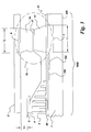
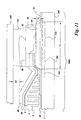
- encapsulating coating 4 is initially deposited on scintillator material 3, detector substrate first portion 150, detector substrate second portion 160, detector substrate adhesive bond area 7, contact pads 21 and non-active underside 200 of detector substrate 1.
- the encapsulating coating tier 126 is selected form a group consisting of poly-para-xylylene material (paryleneTM N), mono-chloro-poly-para-xylylene material (paryleneTM C), di-chloro-poly-para-xylylene material (paryleneTM D), and combinations thereof.
- the encapsulating coating 4 is then typically removed by RIE utilizing an oxygen gas, where the OpticladTM serves the function of the metallic hard mask, form the area designated as T4, detector substrate first portion 150, detector substrate second portion 160, detector substrate adhesive bond area 7, contact pads 21 and non-active underside 200 of detector substrate 1.
- Suitable material choices for corrosion protection layer 50 comprise materials having preferably low X-ray absorption, typically less than about 2% to reduce the degradation of the X ray detector assembly 1000. These low X-ray absorption corrosion protection layer 50 materials typically have a thickness in range between about 1 micron and about 100 microns.
- X-ray detector assembly 1000 of Fig. 8 further typically comprising a protective cover 100 and a protective cover epoxy 110.
- Protective cover 100 is disposed over corrosion protection layer 50 and detector substrate third portion 170.
- Protective cover epoxy 110 is disposed between detector substrate third portion 170 and protective cover 100; protective cover epoxy 110 is disposed between corrosion protection layer 50 disposed over detector substrate second portion 160 and protective cover 100.
- Encapsulating coating 4 is disposed so that it does not extend over detector substrate third portion 170.
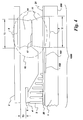
- X-ray detector assembly 1000 of Fig. 8 further typically comprising a protective cover 100 and a protective cover epoxy 110.
- Protective cover 100 is disposed over corrosion protection layer 50 and planarized adhesive layer 80.
- Protective cover epoxy 110 is disposed between planarized adhesive layer 80 and protective cover 100; protective cover epoxy 110 is disposed between corrosion protection layer 50 disposed over detector substrate second portion 160 and protective cover 100.
- Encapsulating coating 4 is disposed so that it does not extend over planarized adhesive layer 80.
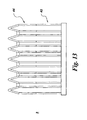
- the step of disposing encapsulating coating 4 of Fig. 8 further comprises disposing first encapsulating coating tier 122 of Fig. 12 (not shown in Fig. 8) on scintillator material 3 of Fig. 8, detector substrate first portion 150, detector substrate second portion 160, detector substrate third portion 170 and contact pads 21. Disposing inner reflective tier 124 of Fig. 12 (not shown in Fig. 8) on first encapsulating coating tier 122; and disposing second encapsulating coating tier 126 of Fig. 12 (not shown in Fig. 8) on inner reflective tier 124.
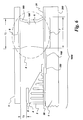
- X-ray detector assembly 1000 is configured as illustrated in Fig. 10 is described below with modifications noted with respect to the embodiment described above as Fig. 8.
- Planarized adhesive layer 80 is disposed on detector substrate second portion 160 and detector substrate third portion 170.
- First planarized adhesive layer bond area 86 is disposed over detector substrate second portion 160.
- Second planarized adhesive layer bond area 87 is disposed over the detector substrate third portion 170.
- Scintillator material 3 is deposited as described above for Fig. 8.
- Encapsulating coating 4 is disposed on scintillator material 3, detector substrate first portion 150 and first planarized adhesive layer adhesive bond area 86, but not so as to extend over second planarized adhesive layer bond area 87.
- Reflective layer 5 is disposed on encapsulating coating 4.
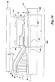
- Planarized adhesive layer 80 is disposed on detector substrate second portion 160 and detector substrate third portion 170.
- Encapsulating coating 4 is disposed on scintillator material 3, detector substrate first portion 150, detector substrate second portion 160, first planarized adhesive layer bond area 86, second planarized adhesive layer bond area 87 and contact pads 21.
- a contact shadow mask (not shown) is then laid down on encapsulating coating 4 on planarized adhesive layer 80, so that contact shadow mask covers contact pads 21 and one edge of contact shadow mask does not extend over first planarized adhesive bond area 86 of planarized adhesive layer 80.
- the reflective layer 5 is then deposited onto encapsulating coating 4 so that no reflective layer 5 is deposited on encapsulating coating 4 that covers second planarized adhesive bond area 87 and contact pads 21.
Landscapes
- Physics & Mathematics (AREA)
- Health & Medical Sciences (AREA)
- Life Sciences & Earth Sciences (AREA)
- General Physics & Mathematics (AREA)
- High Energy & Nuclear Physics (AREA)
- Molecular Biology (AREA)
- Spectroscopy & Molecular Physics (AREA)
- Measurement Of Radiation (AREA)
Applications Claiming Priority (2)
| Application Number | Priority Date | Filing Date | Title |
|---|---|---|---|
| US10/631,197 US7053381B2 (en) | 2001-12-06 | 2003-07-30 | Dual para-xylylene layers for an X-ray detector |
| US631197 | 2003-07-30 |
Publications (3)
| Publication Number | Publication Date |
|---|---|
| EP1503419A2 true EP1503419A2 (fr) | 2005-02-02 |
| EP1503419A3 EP1503419A3 (fr) | 2006-05-31 |
| EP1503419B1 EP1503419B1 (fr) | 2010-12-29 |
Family
ID=33541516
Family Applications (1)
| Application Number | Title | Priority Date | Filing Date |
|---|---|---|---|
| EP04254486A Expired - Lifetime EP1503419B1 (fr) | 2003-07-30 | 2004-07-27 | Couches de double para-xylylène pour un détecteur de rayons x |
Country Status (4)
| Country | Link |
|---|---|
| US (1) | US7053381B2 (fr) |
| EP (1) | EP1503419B1 (fr) |
| JP (1) | JP4512439B2 (fr) |
| DE (1) | DE602004030748D1 (fr) |
Families Citing this family (11)
| Publication number | Priority date | Publication date | Assignee | Title |
|---|---|---|---|---|
| CN1647595A (zh) * | 2002-04-11 | 2005-07-27 | 皇家飞利浦电子股份有限公司 | 电绝缘体和电子器件 |
| JP4112448B2 (ja) * | 2003-07-28 | 2008-07-02 | 株式会社東芝 | 電気光配線基板及び半導体装置 |
| JP5905672B2 (ja) * | 2011-06-28 | 2016-04-20 | 株式会社東芝 | 放射線検出器及びその製造方法 |
| US8415628B1 (en) | 2011-10-31 | 2013-04-09 | General Electric Company | Hermetically sealed radiation detector and methods for making |
| JP6041594B2 (ja) * | 2012-09-14 | 2016-12-14 | 浜松ホトニクス株式会社 | シンチレータパネル、及び、放射線検出器 |
| US9935152B2 (en) | 2012-12-27 | 2018-04-03 | General Electric Company | X-ray detector having improved noise performance |
| US9917133B2 (en) | 2013-12-12 | 2018-03-13 | General Electric Company | Optoelectronic device with flexible substrate |
| US10732131B2 (en) | 2014-03-13 | 2020-08-04 | General Electric Company | Curved digital X-ray detector for weld inspection |
| US9515276B2 (en) | 2014-09-02 | 2016-12-06 | General Electric Company | Organic X-ray detector and X-ray systems |
| US9535173B2 (en) | 2014-09-11 | 2017-01-03 | General Electric Company | Organic x-ray detector and x-ray systems |
| US9513383B1 (en) * | 2015-06-03 | 2016-12-06 | Perkinelmer Holdings, Inc. | Scintillator sealing with foil |
Family Cites Families (21)
| Publication number | Priority date | Publication date | Assignee | Title |
|---|---|---|---|---|
| US4011454A (en) | 1975-04-28 | 1977-03-08 | General Electric Company | Structured X-ray phosphor screen |
| JPH03211757A (ja) | 1989-12-21 | 1991-09-17 | General Electric Co <Ge> | 気密封じの物体 |
| US5153438A (en) | 1990-10-01 | 1992-10-06 | General Electric Company | Method of forming an x-ray imaging array and the array |
| US5187369A (en) | 1990-10-01 | 1993-02-16 | General Electric Company | High sensitivity, high resolution, solid state x-ray imaging device with barrier layer |
| US5171996A (en) | 1991-07-31 | 1992-12-15 | Regents Of The University Of California | Particle detector spatial resolution |
| US5179284A (en) | 1991-08-21 | 1993-01-12 | General Electric Company | Solid state radiation imager having a reflective and protective coating |
| US5132539A (en) | 1991-08-29 | 1992-07-21 | General Electric Company | Planar X-ray imager having a moisture-resistant sealing structure |
| US5227635A (en) | 1991-11-22 | 1993-07-13 | Xsirious, Inc. | Mercuric iodide x-ray detector |
| US5336928A (en) | 1992-09-18 | 1994-08-09 | General Electric Company | Hermetically sealed packaged electronic system |
| US5368882A (en) | 1993-08-25 | 1994-11-29 | Minnesota Mining And Manufacturing Company | Process for forming a radiation detector |
| US5401668A (en) | 1993-09-02 | 1995-03-28 | General Electric Company | Method for fabrication solid state radiation imager having improved scintillator adhesion |
| CA2131243A1 (fr) | 1993-09-27 | 1995-03-28 | Kenneth R. Paulson | Procede pour l'obtention d'un produit phosphorescent |
| US5654084A (en) | 1994-07-22 | 1997-08-05 | Martin Marietta Energy Systems, Inc. | Protective coatings for sensitive materials |
| CN1133881C (zh) | 1997-02-14 | 2004-01-07 | 浜松光子学株式会社 | 放射线检测元件及其制造方法 |
| DE69817035T2 (de) | 1997-02-14 | 2004-06-09 | Hamamatsu Photonics K.K., Hamamatsu | Strahlungsdetektor und Verfahren zu seiner Herstellung |
| JP3405706B2 (ja) * | 1997-02-14 | 2003-05-12 | 浜松ホトニクス株式会社 | 放射線検出素子 |
| JP3924352B2 (ja) | 1997-06-05 | 2007-06-06 | 浜松ホトニクス株式会社 | 裏面照射型受光デバイス |
| JP3789646B2 (ja) * | 1998-06-19 | 2006-06-28 | 浜松ホトニクス株式会社 | 放射線イメージセンサ |
| US6146489A (en) | 1998-11-19 | 2000-11-14 | General Electric Company | Method and apparatus for depositing scintillator material on radiation imager |
| JP3276614B2 (ja) * | 1999-04-22 | 2002-04-22 | 浜松ホトニクス株式会社 | 光学素子、放射線イメージセンサ及び光学素子の製造方法 |
| US6720561B2 (en) * | 2001-12-06 | 2004-04-13 | General Electric Company | Direct CsI scintillator coating for improved digital X-ray detector assembly longevity |
-
2003
- 2003-07-30 US US10/631,197 patent/US7053381B2/en not_active Expired - Lifetime
-
2004
- 2004-07-27 EP EP04254486A patent/EP1503419B1/fr not_active Expired - Lifetime
- 2004-07-27 DE DE602004030748T patent/DE602004030748D1/de not_active Expired - Lifetime
- 2004-07-29 JP JP2004221027A patent/JP4512439B2/ja not_active Expired - Fee Related
Also Published As
| Publication number | Publication date |
|---|---|
| EP1503419B1 (fr) | 2010-12-29 |
| US20040021084A1 (en) | 2004-02-05 |
| JP2005134370A (ja) | 2005-05-26 |
| DE602004030748D1 (de) | 2011-02-10 |
| JP4512439B2 (ja) | 2010-07-28 |
| EP1503419A3 (fr) | 2006-05-31 |
| US7053381B2 (en) | 2006-05-30 |
Similar Documents
| Publication | Publication Date | Title |
|---|---|---|
| US6720561B2 (en) | Direct CsI scintillator coating for improved digital X-ray detector assembly longevity | |
| CA2261663C (fr) | Dispositif de detection de radiations et son procede de production | |
| JP3077941B2 (ja) | 放射線検出素子及びその製造方法 | |
| US6891164B2 (en) | Radiation image sensor and scintillator panel | |
| EP1503419B1 (fr) | Couches de double para-xylylène pour un détecteur de rayons x | |
| US9136029B2 (en) | Scintillator panel, and radiographic image sensor | |
| JPWO1998036291A1 (ja) | 放射線検出素子及びその製造方法 | |
| US20090065705A1 (en) | Scintillator plate | |
| US6940072B2 (en) | Radiation detection device and method of making the same | |
| JPWO2001051951A1 (ja) | 放射線イメージセンサ及びシンチレータパネル | |
| US9223035B2 (en) | Radiographic image detector | |
| JP2000284053A (ja) | 放射線検出素子 | |
| JP4445281B2 (ja) | X線検出器パネル組立体を製造する方法及びデジタルx線パネル | |
| JP4099206B2 (ja) | シンチレータパネル及び放射線イメージセンサ | |
| JP3987438B2 (ja) | シンチレータパネル及び放射線イメージセンサ | |
| JP4057316B2 (ja) | シンチレータパネルおよびその製造方法 | |
| JP3029873B2 (ja) | 放射線検出素子及びその製造方法 |
Legal Events
| Date | Code | Title | Description |
|---|---|---|---|
| PUAI | Public reference made under article 153(3) epc to a published international application that has entered the european phase |
Free format text: ORIGINAL CODE: 0009012 |
|
| AK | Designated contracting states |
Kind code of ref document: A2 Designated state(s): AT BE BG CH CY CZ DE DK EE ES FI FR GB GR HU IE IT LI LU MC NL PL PT RO SE SI SK TR |
|
| AX | Request for extension of the european patent |
Extension state: AL HR LT LV MK |
|
| PUAL | Search report despatched |
Free format text: ORIGINAL CODE: 0009013 |
|
| AK | Designated contracting states |
Kind code of ref document: A3 Designated state(s): AT BE BG CH CY CZ DE DK EE ES FI FR GB GR HU IE IT LI LU MC NL PL PT RO SE SI SK TR |
|
| AX | Request for extension of the european patent |
Extension state: AL HR LT LV MK |
|
| 17P | Request for examination filed |
Effective date: 20061130 |
|
| AKX | Designation fees paid |
Designated state(s): DE FR NL |
|
| 17Q | First examination report despatched |
Effective date: 20070904 |
|
| GRAP | Despatch of communication of intention to grant a patent |
Free format text: ORIGINAL CODE: EPIDOSNIGR1 |
|
| GRAS | Grant fee paid |
Free format text: ORIGINAL CODE: EPIDOSNIGR3 |
|
| GRAA | (expected) grant |
Free format text: ORIGINAL CODE: 0009210 |
|
| AK | Designated contracting states |
Kind code of ref document: B1 Designated state(s): DE FR NL |
|
| REF | Corresponds to: |
Ref document number: 602004030748 Country of ref document: DE Date of ref document: 20110210 Kind code of ref document: P |
|
| REG | Reference to a national code |
Ref country code: DE Ref legal event code: R096 Ref document number: 602004030748 Country of ref document: DE Effective date: 20110210 |
|
| REG | Reference to a national code |
Ref country code: NL Ref legal event code: T3 |
|
| PLBE | No opposition filed within time limit |
Free format text: ORIGINAL CODE: 0009261 |
|
| STAA | Information on the status of an ep patent application or granted ep patent |
Free format text: STATUS: NO OPPOSITION FILED WITHIN TIME LIMIT |
|
| 26N | No opposition filed |
Effective date: 20110930 |
|
| REG | Reference to a national code |
Ref country code: DE Ref legal event code: R097 Ref document number: 602004030748 Country of ref document: DE Effective date: 20110930 |
|
| REG | Reference to a national code |
Ref country code: FR Ref legal event code: PLFP Year of fee payment: 13 |
|
| REG | Reference to a national code |
Ref country code: FR Ref legal event code: PLFP Year of fee payment: 14 |
|
| REG | Reference to a national code |
Ref country code: FR Ref legal event code: PLFP Year of fee payment: 15 |
|
| P01 | Opt-out of the competence of the unified patent court (upc) registered |
Effective date: 20230528 |
|
| PGFP | Annual fee paid to national office [announced via postgrant information from national office to epo] |
Ref country code: NL Payment date: 20230622 Year of fee payment: 20 |
|
| PGFP | Annual fee paid to national office [announced via postgrant information from national office to epo] |
Ref country code: FR Payment date: 20230724 Year of fee payment: 20 Ref country code: DE Payment date: 20230620 Year of fee payment: 20 |
|
| REG | Reference to a national code |
Ref country code: DE Ref legal event code: R071 Ref document number: 602004030748 Country of ref document: DE |
|
| REG | Reference to a national code |
Ref country code: NL Ref legal event code: MK Effective date: 20240726 |