EP1505687A1 - Résonateur diélectrique, filtre diélectrique et méthode de support d'un élément résonateur diélectrique - Google Patents
Résonateur diélectrique, filtre diélectrique et méthode de support d'un élément résonateur diélectrique Download PDFInfo
- Publication number
- EP1505687A1 EP1505687A1 EP04018401A EP04018401A EP1505687A1 EP 1505687 A1 EP1505687 A1 EP 1505687A1 EP 04018401 A EP04018401 A EP 04018401A EP 04018401 A EP04018401 A EP 04018401A EP 1505687 A1 EP1505687 A1 EP 1505687A1
- Authority
- EP
- European Patent Office
- Prior art keywords
- dielectric
- cover
- resonance element
- flat surfaces
- pair
- Prior art date
- Legal status (The legal status is an assumption and is not a legal conclusion. Google has not performed a legal analysis and makes no representation as to the accuracy of the status listed.)
- Withdrawn
Links
Images


Classifications
-
- H—ELECTRICITY
- H01—ELECTRIC ELEMENTS
- H01P—WAVEGUIDES; RESONATORS, LINES, OR OTHER DEVICES OF THE WAVEGUIDE TYPE
- H01P7/00—Resonators of the waveguide type
- H01P7/10—Dielectric resonators
Definitions
- the present invention relates to a dielectric resonator and a dielectric filter for use in a base station for mobile communication such as portable telephone, a transmitting station for broadcasting, and the like, and to a method of supporting a dielectric resonance element used in the dielectric resonator and the dielectric filter.
- a filter for use in a base station should have a low-loss transmission characteristic such as to cause substantially no degradation in signal components and a sharp attenuation characteristic such as to reliably remove unnecessary interfering wave components. Also, there has been an increasing demand for reducing the size as well as improving electrical characteristics.
- An example of filters capable of meeting such a demand is a TM mode dielectric filter using a TM mode dielectric resonator of a high Q-value.
- Fig. 9(a) is a cross-sectional view of a conventional TM mode dielectric resonator
- Fig. 9(b) is a cross-sectional view of the conventional TMmode dielectric resonator taken along the line B-B' in Fig. 9 (a) and seen from a position above the resonator
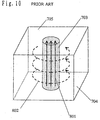
- Fig. 10 shows an electromagnetic field distribution in the conventional dielectric resonator.
- the dielectric resonator has input/output terminals 701a and 701b, input/output probes 702a and 702b, a dielectric resonance element 703, a metallic casing 704, a metallic cover 705; connecting screws 706, and a frequency adjusting screw 707.
- Arrow 801 indicates an electric force line and arrow 802 indicates a magnetic force line.
- Input/output probes 702a and 702b are connected to center conductors of the input/output terminals 701a and 701b by soldering or the like.
- the dielectric resonance element 703 has a cylindrical shape, is placed substantially at a center of the casing 704, and is pinched between a bottom surface 710 of the casing 704 and the metallic cover 705, with its upper flat surface 709 placed on the metallic cover 705 and its lower flat surface 712 placed on the bottom surface 710.
- the casing 704 and the metallic cover 705 are fixed on each other by connecting screws 706 to improve the degree of contact for connection between the lower flat surface 712 of the dielectric resonance element 703 and the bottom surface 710 of the casing 704 and the degree of contact for connection between the upper flat surface 709 of the dielectric resonance element 703 and the metallic cover 705 and to improve the reliability of connection between the casing 704 and the metallic cover 705 so that the discontinuity of current flowing through the connecting portions is reduced.
- An inner hole 711 is formed in the cylindrical dielectric resonance element 703.
- the frequency adjusting screw 707 connected to the casing 704 is inserted in the inner hole 711 in which electric force lines 801 are concentrated to change the resonance frequency of the dielectric resonator.
- a signal input to the input/output terminal 701a is transferred by electromagnetic coupling between the input/output probe 702a and the dielectric resonance element 703 and electromagnetic coupling between the dielectric resonance element 703 and the input/output probe 702b to be output through the input/output terminal 701b.
- this dielectric resonator operates as a TM010 mode dielectric resonator (e.g. , see Japanese Patent Publication No. 63-22727, Japanese Patent Publication No. 63-22728, and Japanese Patent Publication No. 63-22729).
- the conductance of the electroconductive film is lower than that of the metallic casing 704 and the influence on the performance of the resonator of the loss due to the current flowing through the electroconductive film is considerably large, so that the Q-value representing the performance of the resonator is reduced. For this reason, it is difficult to realize a high-performance dielectric resonator and a high-performance filter.
- an object of the present invention is to provide a dielectric filter capable of operating with stability even when a change in temperature occurs, and a method of supporting a dielectric resonance element of the dielectric filter.
- the 1 st aspect of the present invention is a dielectric resonator comprising:
- the 2 nd aspect of the present invention is the dielectric resonator according to the 1 st aspect of the present invention, wherein the other of said pair of flat surfaces or an edge portion thereof is covered with an electroconductive film.
- the 3 rd aspect of the present invention is the dielectric resonator according to the 2 nd aspect of the present invention, wherein said electroconductive film isformed bymetalization.
- the 4 th aspect of the present invention is the dielectric resonator according to the 2 nd aspect of the present invention, wherein said resilient portion and the edge portion of the other of said flat surfaces contact in a line contact manner.
- the 5 th aspect of the present invention is the dielectric resonator according to the 1 st aspect of the present invention, wherein a hole having a size not exceeding the size of the other of said pair of flat surfaces is formed in said cover, wherein the other of said pair of flat surfaces or the edge portion thereof contacts a portion on the periphery of said hole so as to close said hole, and wherein the portion on the periphery of the hole in said cover is warped according to relative expansion of the dielectric resonance element in the axial direction due to a change in temperature to increase the biasing force.
- the 6 th aspect of the present invention is the dielectric resonator according to the 5 th aspect of the present invention, wherein the thickness of the portion on the periphery of said hole is smaller than the other portion of said cover.
- the 7 th aspect of the present invention is the dielectric resonator according to the 6 th aspect of the present invention, wherein the portion on the periphery of said hole is formed by countersinking said cover on the side where the other of said pair of flat surfaces contacts said cover.
- the 8 th aspect of the present invention is the dielectric resonator according to the 5 th aspect of the present invention, wherein another cover is provided over said cover so as to cover said hole.
- the 9 th aspect of the present invention is the dielectric resonator according to the 6 th aspect of the present invention, wherein the portion on the periphery of said hole and the other portionof said cover connected to each other with being rounded at the connection so as not to form an edge in said casing.
- the 10 th aspect of the present invention is a dielectric resonator comprising:
- the 11 th aspect of the present invention is the dielectric resonator according to the 10 th aspect of the present invention, wherein a recess having a size exceeding the size of the other of said flat surfaces are formed in said cover, and a thin film having electroconductivity and ductility is stretched so as to cover said recess, wherein an electroconductive film is formed on a portion in a side portion adjacent to the other of said pair of flat surfaces of said dielectric resonance element, and wherein said electroconductive film is connected to said thin film by solder or an electroconductive adhesive.
- the 12 th aspect of the present invention is the dielectric resonator according to the 11 th aspect of the present invention, wherein said electroconductive film is formedbymetalization.
- the 13 th aspect of the present invention is the dielectric resonator according to the 10 th aspect of the present invention, wherein a hole having a size substantially equal to the size of the other of said flat surfaces is formed in said cover, wherein an electroconductive film is formed on the other of said pair of flat surfaces of said dielectric resonance element and on a portion in a side portion adjacent to the other of said pair of flat surfaces, and wherein said electroconductive film is connected to a portion on the periphery of said hole by solder or an electroconductive adhesive.
- the 14 th aspect of the present invention is the dielectric resonator according to the 13 th aspect of the present invention, wherein the thickness of the portion on the periphery of said hole is smaller than the other portion of said cover.
- the 15 th aspect of the present invention is a dielectric filter comprises dielectric resonators according to the 1 st or the 10 th aspect of the present invention, the dielectric resonators being connected one after another to form a plurality of stages.
- the 16 th aspect of the present invention is a method of supporting a dielectric resonance element comprising:
- the 17 th aspect of the present invention is a method of supporting a dielectric resonance element comprising:
- a dielectric resonator capable of operating with stability even when a change in temperature occurs, a dielectric filter using the dielectric resonator, a method of supporting a dielectric resonance element of the dielectric resonator can be provided.
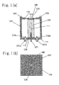
- Fig. 1(a) is a cross-sectional view of a TMmode dielectric resonator in Embodiment 1 of the present invention.
- Fig. 1 (b) is a top view of the dielectric resonator.
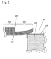
- Fig. 2 is an enlarged sectional view of a metalized surface 108, which is an example of the electroconductive film in accordance with the present invention in a dielectric resonance element, and which is provided in a dielectric resonance element 103 used in the dielectric resonator in Embodiment 1 of the present invention. Referring to Figs.
- the dielectric resonator includes input/output terminals 101a and 101b, input/output probes 102a and 102b, a dielectric resonance element 103, a metallic casing 104, a metallic cover 105, connecting screws 106, a frequency adjusting screw 107, and the metalized surface 108, and the metallic cover 105 has a thick portion 201 and a thin portion 202.
- the dielectric resonance element 103 has an upper flat surface 109 in its upper portion, which is an example of one of the flat surfaces in accordance with the present invention, and a lower flat surface 112 in its lower portion, which is placed opposite from the upper flat surface 109, and which is an example of the other of the flat surfaces in accordance with the present invention.
- To form the thin portion 202 in the metallic cover 105 countersinking is performed on an upper portion of on a plate having a thickness equal to that of the thick portion 201 to a depth corresponding to the difference between the thick portion 201 and the thin portion 202.
- the metallic casing 104 such as copper (its linear expansion coefficient:16.5ppm/°C), aluminum (23.1ppm/°C), silver (18.9ppm/°C), brass (17.5 ppm/°C), iron (11. 8 ppm/°C), phosphor bronze (ppm/°C) might be used.
- a material of a dielectric resonance element 103 one with its linear expansion coefficient is, for example, between 3 and 15 might be used.
- the input/output probes 102a and 102b are connected to center conductors of the input/output terminals 101a and 101b by soldering or the like.
- the dielectric resonance element 103 is, for example, cylindrical, and the upper flat surface 109 and the lower flat surface 112 are metalized with a metal having high conductivity such as gold, silver or copper, as shown in Fig. 2. Also in the side surface of the dielectric resonance element 103, partial side surface regions respectively connected to the upper flat surface 109 and the lower flat surface 112 are metalized with the same metal.
- the current flowing through the inner wall of the metallic casing 104 largely influences the Q-value representing the performance of the resonator because of a characteristic of the TM mode.
- a casing made of copper or aluminum and plated with silver is used as the metallic casing 104 and a countersunk slightly larger than the flat surface of the dielectric resonance element 103 is provided in a central portion of a bottom surface 110 of the metallic casing 104.
- the dielectric resonance element 103 is placed at a center of the metallic casing 104 by being fitted in the countersunk.
- the dielectric resonance element 103 is placed in the metallic casing 104 in this manner, the metallic cover 105 is then placed on the dielectric resonance element 103 and the metallic casing 104, and the metallic casing 104 and the metallic cover 105 are connected to each other by connecting screws 106.
- the height of the dielectric resonance element 103 is set to such a value that the dielectric resonance element 103 protrudes slightly beyond the frame upper end of the metallic casing 104, and that the protrusion is maintained in a temperature range in which the dielectric resonator is supposed to be used.
- the thin portion 202 of the metallic cover 105 is warped according to the length of the above-described protrusion when the metallic casing 104 and the metallic cover 105 are connected by screwing with the connecting screws 106. That is, the thin portion 202 is warped in the above-described manner to press the upper flat surface 109 of the dielectric resonance element 103 by a biasing force.
- the thick portion 201 is provided adj acent to the thin portion 202 in the metallic cover 105.
- a hole 120 having a diameter smaller than the outside diameter of the dielectric resonance element 103 is formed in the metallic cover 105 at a center of the same.
- the thin portion 202 (the portion around the hole 120 that the dielectric resonance element 103 contacts) forms the resilient portion in accordance with the present invention or the thin portion 202 and the thick portion 201 (the portion other than the portion around the hole 120) form the resilient portion in cooperation with each other to press the upper flat surface 109 by the biasing force so as to follow the expansion/contraction of the dielectric resonance element 103.
- the expansion coefficient of the metallic casing 104 is larger than that of the dielectric resonance element 103.
- the expansion coefficient of the metallic casing 104 is smaller than that of the dielectric resonance element 103, a larger force based on the resilience is applied to the dielectric resonance element 103 when the ambient temperature rises.
- the current path connecting the metallic cover 105 and the metalized surface 108 is formed only at an outer circumferential portion (edge) of the metalized surface 108. That is, the metallic cover 105 and the metalized surface 108 contact in a line contact manner. Even when the ambient temperature changes, this line contact is maintained and there is no electrical characteristic problem. Therefore, this line contact is preferable. If the metallic cover 105 and the metalized surface 108 contact in a surface contact manner, the metalized surface 108 is separated to cause a change in electrical characteristic when the ambient temperature changes.
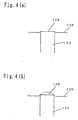
- Fig. 4(a) schematically shows a state where the metallic cover 105 and the metalized surface 108 contact in a surface contact manner
- Fig. 4(a) schematically shows a state where the metallic cover 105 and the metalized surface 108 contact in a surface contact manner
- FIG. 4(b) schematically shows the condition of the surface contact when the ambient temperature changes in the state shown in Fig. 4(a).
- the dielectric resonance element 103 expands for example.
- a force is thereby applied to the metallic cover 105 to deform the same above the metalized surface 108, as indicated by the broken line in Fig. 4(b).
- this force is applied, the metalized surface 108 can be easily separated from the dielectric resonance element 103.
- An inner hole 111 which is formed so as not to extend through the entire length of the dielectric resonance element 103, is provided in the dielectric resonance element 103.
- the frequency adjusting screw 107 connected to the metallic casing 104 is inserted to enable the resonance frequency of the dielectric resonator to be changed.
- a signal input to the input/output terminal 101a is transferred by electromagnetic coupling between the input/output probe 102a and the dielectric resonance element 103 and electromagnetic coupling between the dielectric resonance element 103 and the input/output probe 102b to be output through the input/output terminal 101b.
- this dielectric resonator operates as a TM010 mode dielectric resonator.
- each of the upper flat surface 109 and the lower flat surface 112 of the dielectric resonance element 103 is metalized. Therefore, even when the ambient temperature changes, no gap occurs between the metalized surface 108 functioning as a ground electrode and the upper flat surface 109 of the dielectric resonance element 103 and between the metalized surface 108 and the lower flat surface 112. Since there is a difference between the linear expansion coefficients of the dielectric resonance element 103 and the metallic casing 104, the dielectric resonance element 103, for example, expands in the axial direction relative to the metallic casing 104 when the ambient temperature changes. However, the amount of expansion is absorbed by a warp of the thin portion 202 of the metallic cover 105. Therefore, dielectric resonator can be made always stable in characteristics even when the temperature of the dielectric resonator is changed.
- the contact between the upper flat surface 109 of the dielectric resonance element 103 and the ground electrode and the contact between the lower flat surface 112 and the ground electrode are very important. If a gap occurs therebetween, the resonance frequency and the Q-value are largely changed. Wave vectors in the TM010 mode have only components in the radial direction and the resonance frequency of the dielectric resonator is independent of the height of the dielectric resonance element 103.
- a method of producing a characteristic effect not in the radial direction but in the height direction of the dielectric resonance element 103 is used as a method for ensuring contact between the upper flat surface 109 of the dielectric resonance element 103 and the ground electrode and contact between the lower flat surface 112 and the ground electrode at all times with stability, thereby enabling stabilization of the resonance frequency of the dielectric resonator.
- the outer circumferential portion of the metalized surface 108 of 'the dielectric resonance element 103 and the metallic cover 105 can be maintained in contact with each other at all times under any temperature condition by the biasing force of the resilient portion formed in the metallic cover 105. Therefore, a dielectric resonator and a dielectric filter can be provided which are free from discontinuity of the current path, and which have improved temperature characteristics and high reliability.
- the structure for absorbing the difference between the linear expansion coefficients of the dielectric resonance element 103 and the metallic casing 104 is provided above the dielectric resonance element 103, because the frequency adjusting screw 107 is provided in and below a lower portion of the dielectric resonance element 103.
- the same effects can also be obtained in a case where the structure for absorbing the difference between the linear expansion coefficients of the dielectric resonance element 103 and the metallic casing 104 is placed below the dielectric resonance element 103, and the frequency adjusting screw 107 is placed above the dielectric resonance element 103.
- the arrangement may be such that not a portion of the metallic cover 105 but a portion of the bottom surface 110 (bottom portion) is warped to apply a biasing force to the lower flat surface 112 of the dielectric resonance element 103.
- the overall height of the dielectric resonator can be reduced in this manner.
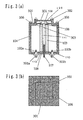
- a projection 203 shown in Fig. 2 at which the thick portion 201 and the thin portion 202 connect to each other, exists inside the casing, current concentration occurs thereon to cause a reduction in the Q-value of the dielectric resonator. Therefore, the projection 203 is rounded to form a rounded portion 303, as shown in Figs. 3 (a) and 3 (b) , thereby enabling the dielectric resonator to be reduced in height without reducing the Q-value.
- the metallic cover 105 is formed only of the thin portion 202 without providing the thick portion 201, the metallic cover 105 can be also warped, although the resiliency in this arrangement differs from that in the above-described arrangement. In this manner, a dielectric resonator in which a biasing force is applied to the dielectric resonance element 103 at any temperature to ensure stabilized characteristics can be provided, as is that described above.
- dielectric resonance element 103 is cylindrical in the above-described arrangement, a dielectric resonator having a dielectric resonance element 103 in the form of a rectangular block can also operate as a TM mode dielectric resonator.
- the dielectric resonance element 103 may be placed in any direction if a structure capable of absorbing expansion/contraction of the dielectric resonance element 103 due to a change in ambient temperature is provided.
- Fig. 6 is a cross-sectional view of a TM mode dielectric resonator in Embodiment 2 of the present invention. Description of the same portions as those in Embodiment 1 will not be repeated.
- the dielectric resonator includes copper foil 401, which is an example of the thin film in accordance with the present invention, solder 402, and a cover 403.
- a metalized surface 108 at the lower end of a dielectric resonance element 103 and a bottom surface 110 of a metallic casing 104 are electrically connected to each other by solder 402.
- Copper foil 401 is provided at the upper end of the dielectric resonance element 103, and the copper foil 401 and the metalized surface 108 at the upper end of the dielectric resonance element 103 are electrically connected to each other by solder 402.
- the copper foil 401 and the metallic casing 104 are connected with reliability by screwing connecting screws 106 from above the cover 403.
- the difference between the linear expansion coefficients of the dielectric resonance element 103 and the metallic casing 104 in the height direction can be absorbed by warpage (i.e., ductility) of the copper foil 401. That is, even when the ambient temperature changes to cause expansion/contraction of the dielectric resonance element 103, the copper foil 401 is warped upwardly or downwardly to maintain connection between the upper flat surface 109 of the dielectric resonance element 103 and the copper foil 401. Therefore, no gap occurs between the dielectric resonance element 103 and the upper metalized surface 108 and there is no considerable influence on the resonance frequency and the Q-value. Also, the dielectric resonator can stand a heat cycle test and has improved reliability.
- warpage i.e., ductility
- the cover 403 may be made of any material selected from metals and nonmetallic materials. However, the cover 403 needs to have solidity such as not to be deformed due to a change in temperature, an impact, or any other action.
- the cover 403 is provided to improve the reliability of connection between the metallic casing 104 and the copper foil 401. Even if a hole is formed in the cover 403 at a center of the same, stabilized characteristics can also be obtained.
- the frequency adjusting screw 107 maybe inserted in this hole.
- the same effects can be obtained irrespective of the diameter of a countersunk 404 provided in the cover 403 if the diameter of the countersunk 404 is smaller than the size of the cavity of the metallic casing 104 and is larger than the outside diameter of the dielectric resonance element 103.
- Fig. 7 is a cross-sectional view of a TM mode dielectric resonator in Embodiment 3 of the present invention. Description of the same portions as those in Embodiments 1 and 2 will not be repeated.
- a thin portion 522 is provided in a metallic cover 501, a metalized surface 108 at the lower end of a dielectric resonance element 103 and a bottom surface 110 of a metallic casing 104 are electrically connected to each other by solder 402, and the metalized surface 108 at the upper end of the dielectric resonance element 103 and the thin portion 522 of the metallic cover 501 are electrically connected to each other by using solder 402.
- the difference between the vertical lengths of the metallic cas ing 104 and the dielectric resonance element 103 at the time of expansion/contraction can be absorbed, as is that in the dielectric resonator in Embodiment 2.
- Either of the metalized surface 108 provided on the upper flat surface 109 of the dielectric resonance element 103 and the metalized surface 108 extending on the side surface of the dielectric resonance element 103 may be soldered to the thin portion 522 of the metallic cover 501.
- Fig. 8(a) is a cross-sectional view of the dielectric filter of the present invention
- Fig. 8(b) is a top cross-sectional view taken along the line A-A' in Fig. 8 (a) . Description of the same portions as those in Embodiment 1 will not be repeated. Referring to Figs.
- the dielectric filter has input/output terminals 601a and 601b, input/output probes 602a and 602b, dielectric resonance elements 603, 603a, 603b, 603c, and 603d, a metallic casing 604, a metallic cover 605, connecting screws 606, frequency adjustingscrews 607a, 607b, 607c, and607d, metalized surfaces 608, interstage-coupling adjusting screws 609a, 609b and 609c and partition walls 610,
- the input/output terminals 601a and 601b are positioned on side portions of the metallic casing 604.
- Each of the input/output probes 602a and 602b connected to center conductors of the input/output terminals 601a and 601b extends in the form of a plate in the same direction as the center conductor, is bent through ninety degrees at a position in the vicinity of the dielectric resonance element 603, and is electrically connected to a bottom surface 910 of the metallic casing 604 by fastening with a screw or soldering for example.
- Each input/output coupling is determined by the thickness and width of the plate of the input/output probe 602a or 602b and the distance between the input/output probe 602a or 602b and the dielectric resonance element 603a or 603d.
- Interstage couplings between the dielectric resonance elements 603a to 603d are determined by the intervals between the dielectric resonance elements and the lengths of the partition walls 610. Interstage couplings therebetween are respectively adjusted finely with the interstage-coupling adjusting screws 609a to 609c.
- the resonance frequencies of the dielectric resonance element 603a to 603d are respectively adjusted with the frequency adjusting screws 607a to 607d.
- the input/output couplings, the interstage couplings and the resonance frequencies of the dielectric resonators are suitably adjusted to realized a dielectric filter having 4-stage bandpass filter characteristics.
- a reliable dielectric filter can be obtained in which stabilized characteristics can be realized even when the temperature of the filter is changed and which can stand a heat cycle test.
- the dielectric filter of the present invention can have stabilized characteristics as a filter having a plurality of stages not limited to four stages.
- the dielectric resonance element 103 of the dielectric resonator in Embodiment 1 a cylindrical dielectric resonance element having a resonance frequency in the 2 GHz band, a specific dielectric constant of about 40, an outside diameter of 9 mm and' a height of 32.00 mm was used.
- the upper flat surface 109 and the lower flat surface 112 of the dielectric resonance element 103 were metalized with gold to a thickness of about 10 to 40 ⁇ m.
- Side surface regions having a width of about 0.3 to 1 mm from the upper flat surface 109 and the lower flat surface 112 were also metalized in the same manner.
- a member made of copper and plated with silver was used as the metallic casing 104, and a countersunk having a diameter of 9.2 mm and a depth of 0.3 mm was provided in the bottom surface 110 of the metallic casing 104 at the center of the same.
- the dielectric resonance element 103 was placed at the center of the metallic casing 104 by being fitted in this countersunk.
- the distance between the upper end surface of the metallic casing 104 and the bottom surface of the countersunk bottom having a depth of 0.3 mm was set to 31.7 mm.
- the dielectric resonance element 103 since the height of the dielectric resonance element 103 is 32.00 mm, the dielectric resonance element 103 protrudes beyond the frame upper end of the metallic casing 104 by 0.3 mm, and the thin portion 202 of the metallic cover 105 is warped by an amount corresponding to the 0.3 mm protrusion when the metallic casing 104 and the metallic cover 105 are fastened to each other with connecting screws 106.
- This dielectric resonator was subjected to a heat cycle test in which a temperature change from -40 to 80°C was caused many times. The results of this test show that the dielectric resonator in accordance with Embodiment 1 has high reliability such as to stand this temperature change.
- the dielectric resonance element 103 of the dielectric resonator in Embodiment 2 the same dielectric resonance element as that in Example 1 was used and copper foil 401 having a thickness of 0.05 mm was used. It was found that even when the dielectric resonance element 103 expanded or contracted due to a change in ambient temperature, no gap occurred between the dielectric resonance element 103 and the upper metalized surface 108 and there was no considerable influence on the resonance frequency and the Q-value. It was also found that the dielectric resonator in accordance with Embodiment 2 had high reliability such as to stand the heat cycle test.
- the dielectric resonator in the above-described examples has a size and uses materials such as to have a resonance frequency in the 2 GHz band. Needless to say, this is only an example of the present invention and the same effects can also be obtained when the size and the materials are changed with a different resonance frequency.
- each dielectric resonance element may expand relative to the metallic casing when it contracts due to a change in temperature. Conversely, each dielectric resonance element may contract relative to the metallic casing when it expands due to a change in temperature. Even in such cases, the same effects can be obtained as long as the same operation as that described above is performed.
- the dielectric resonator in accordance with the present invention or a device using a dielectric resonance element supported by the dielectric resonance element supporting method in accordance with the present invention is capable of operating with stability even when the temperature thereof is changed and is advantageously used as a dielectric resonator, dielectric filter or the like in a base station for mobile communication such as portable telephone, a transmitting station for broadcasting, and the like.
Landscapes
- Control Of Motors That Do Not Use Commutators (AREA)
Applications Claiming Priority (2)
| Application Number | Priority Date | Filing Date | Title |
|---|---|---|---|
| JP2003286137 | 2003-08-04 | ||
| JP2003286137 | 2003-08-04 |
Publications (1)
| Publication Number | Publication Date |
|---|---|
| EP1505687A1 true EP1505687A1 (fr) | 2005-02-09 |
Family
ID=33549999
Family Applications (1)
| Application Number | Title | Priority Date | Filing Date |
|---|---|---|---|
| EP04018401A Withdrawn EP1505687A1 (fr) | 2003-08-04 | 2004-08-03 | Résonateur diélectrique, filtre diélectrique et méthode de support d'un élément résonateur diélectrique |
Country Status (3)
| Country | Link |
|---|---|
| US (1) | US7106152B2 (fr) |
| EP (1) | EP1505687A1 (fr) |
| CN (1) | CN1581569A (fr) |
Cited By (9)
| Publication number | Priority date | Publication date | Assignee | Title |
|---|---|---|---|---|
| EP1755189A1 (fr) | 2005-08-18 | 2007-02-21 | Matsushita Electric Industrial Co., Ltd. | Filtre à micro-ondes avec charges dieléctriques de la même hauteur comme boîtier de filtre |
| WO2009142560A1 (fr) * | 2008-05-21 | 2009-11-26 | Telefonaktiebolaget L M Ericsson (Publ) | Système de distribution de force pour des filtres radiofréquence |
| EP2538487A1 (fr) * | 2011-06-24 | 2012-12-26 | CommScope Italy S.r.l. | Résonateur diélectrique indépendant de la température |
| EP2605330A4 (fr) * | 2010-09-03 | 2013-07-03 | Huawei Tech Co Ltd | Résonateur diélectrique à mode magnétique transverse, filtre diélectrique à mode magnétique transverse et station de base |
| GB2499724A (en) * | 2012-02-24 | 2013-08-28 | Radio Design Ltd | Cavity filter comprising dielectric rod and flexible lid to compensate for mechanical tolerances |
| CN104885294A (zh) * | 2012-08-13 | 2015-09-02 | 诺基亚通信公司 | 电介质滤波器 |
| WO2017088195A1 (fr) * | 2015-11-28 | 2017-06-01 | 华为技术有限公司 | Résonateur diélectrique et filtre |
| GB2505873B (en) * | 2012-08-07 | 2019-10-02 | Filtronic Wireless Ltd | A microwave TM mode resonator and an electrical filter including such a resonator |
| EP4096015A4 (fr) * | 2020-08-07 | 2023-09-06 | Wuguang System Company Limited | Unité de résonance et filtre diélectrique |
Families Citing this family (22)
| Publication number | Priority date | Publication date | Assignee | Title |
|---|---|---|---|---|
| US7570136B2 (en) * | 2006-09-20 | 2009-08-04 | Alcatel-Lucent Usa Inc. | Re-entrant resonant cavities, filters including such cavities and method of manufacture |
| CN101978551A (zh) * | 2007-12-13 | 2011-02-16 | 天瑞通讯产品有限公司 | 微波滤波器 |
| US8773222B2 (en) * | 2008-01-31 | 2014-07-08 | Telefonaktiebolaget L M Ericsson (Publ) | Filter assembly |
| KR101072284B1 (ko) * | 2008-08-01 | 2011-10-11 | 주식회사 케이엠더블유 | 고주파 필터의 유전체 공진기 및 그 조립 방법 |
| CN101546857B (zh) * | 2009-04-21 | 2012-11-07 | 华为技术有限公司 | 一种介质谐振器及其装配方法、介质滤波器 |
| CN101895004A (zh) * | 2010-03-17 | 2010-11-24 | 深圳市大富科技股份有限公司 | 介质谐振器、弹性导电屏蔽件和介质滤波器 |
| CN101826649A (zh) * | 2010-04-27 | 2010-09-08 | 江苏江佳电子股份有限公司 | 一种tm模介质谐振器 |
| CN102148417B (zh) * | 2010-08-18 | 2014-04-09 | 深圳市大富科技股份有限公司 | 介质滤波器、介质谐振器及盖板单元和通信设备 |
| CN102025008B (zh) * | 2010-12-06 | 2013-09-04 | 深圳市大富科技股份有限公司 | 介质滤波器、介质谐振杆安装结构以及通信设备 |
| CN102623785B (zh) * | 2011-01-28 | 2015-09-09 | 深圳市大富科技股份有限公司 | 介质滤波器、介质谐振器、盖板单元及通信设备 |
| CN102544648B (zh) * | 2011-12-29 | 2014-04-16 | 华为技术有限公司 | 一种介质滤波器及多工器 |
| CN103855455B (zh) * | 2012-11-30 | 2018-05-22 | 深圳光启创新技术有限公司 | 一种谐振子、谐振腔、滤波器件及电磁波设备 |
| CN103872419A (zh) * | 2012-12-11 | 2014-06-18 | 中兴通讯股份有限公司 | 一种介质谐振器及其装配方法及介质滤波器 |
| WO2015100597A1 (fr) * | 2013-12-31 | 2015-07-09 | 华为技术有限公司 | Résonateur diélectrique, filtre diélectrique et dispositif de communication |
| US9742050B2 (en) * | 2014-01-17 | 2017-08-22 | Alcatel-Lucent Shanghai Bell Co., Ltd. | Methods and devices for grounding deep drawn resonators |
| CN104979609A (zh) * | 2014-04-01 | 2015-10-14 | Ace技术株式会社 | 腔体滤波器 |
| KR20160118667A (ko) * | 2015-04-02 | 2016-10-12 | 한국전자통신연구원 | 공진기 필터 |
| CN105140615B (zh) * | 2015-09-18 | 2018-09-25 | 武汉凡谷陶瓷材料有限公司 | 超小型介质谐振器 |
| EP3565054B1 (fr) | 2017-01-18 | 2022-05-04 | Huawei Technologies Co., Ltd. | Résonateur diélectrique à mode magnétique transversal, filtre et dispositif de communication |
| WO2020133181A1 (fr) | 2018-12-28 | 2020-07-02 | 华为技术有限公司 | Filtre en mode tm et son procédé de fabrication |
| CN114976538A (zh) * | 2022-05-07 | 2022-08-30 | 成都领益通信技术有限公司 | 滤波器 |
| CN115642426A (zh) * | 2022-10-27 | 2023-01-24 | 中国电子科技集团公司第十三研究所 | 一种介质谐振器用连接插芯 |
Citations (5)
| Publication number | Priority date | Publication date | Assignee | Title |
|---|---|---|---|---|
| US4639699A (en) * | 1982-10-01 | 1987-01-27 | Murata Manufacturing Co., Ltd. | Dielectric resonator comprising a resonant dielectric pillar mounted in a conductively coated dielectric case |
| GB2188789A (en) * | 1986-04-07 | 1987-10-07 | Motorola Inc | R.F. ceramic resonator filter; microstrip combiner |
| EP1148574A2 (fr) * | 2000-03-30 | 2001-10-24 | Murata Manufacturing Co., Ltd. | Résonateur diélectrique, filtre, duplexeur et dispositif de communication |
| JP2002094308A (ja) * | 2000-09-20 | 2002-03-29 | Hitachi Kokusai Electric Inc | Tmモード誘電体共振器 |
| US20030058067A1 (en) * | 2001-09-27 | 2003-03-27 | Hiroki Wakamatsu | Dielectric resonator, filter, duplexer and communication device |
Family Cites Families (5)
| Publication number | Priority date | Publication date | Assignee | Title |
|---|---|---|---|---|
| JPS6322728A (ja) | 1986-07-15 | 1988-01-30 | Nissan Motor Co Ltd | キヤンバストツプのシ−ル構造 |
| JPS6322727A (ja) | 1986-07-15 | 1988-01-30 | Omron Tateisi Electronics Co | 接触感応制御装置 |
| JPS6322729A (ja) | 1986-07-15 | 1988-01-30 | Nissan Motor Co Ltd | 四輪駆動車用トランスフア |
| FR2646022B1 (fr) * | 1989-04-13 | 1991-06-07 | Alcatel Espace | Filtre a resonateur dielectrique |
| DE60141555D1 (de) * | 2000-06-15 | 2010-04-29 | Panasonic Corp | Resonator und Hochfrequenzfilter |
-
2004
- 2004-08-03 EP EP04018401A patent/EP1505687A1/fr not_active Withdrawn
- 2004-08-03 CN CN200410055909.3A patent/CN1581569A/zh active Pending
- 2004-08-03 US US10/911,078 patent/US7106152B2/en not_active Expired - Lifetime
Patent Citations (5)
| Publication number | Priority date | Publication date | Assignee | Title |
|---|---|---|---|---|
| US4639699A (en) * | 1982-10-01 | 1987-01-27 | Murata Manufacturing Co., Ltd. | Dielectric resonator comprising a resonant dielectric pillar mounted in a conductively coated dielectric case |
| GB2188789A (en) * | 1986-04-07 | 1987-10-07 | Motorola Inc | R.F. ceramic resonator filter; microstrip combiner |
| EP1148574A2 (fr) * | 2000-03-30 | 2001-10-24 | Murata Manufacturing Co., Ltd. | Résonateur diélectrique, filtre, duplexeur et dispositif de communication |
| JP2002094308A (ja) * | 2000-09-20 | 2002-03-29 | Hitachi Kokusai Electric Inc | Tmモード誘電体共振器 |
| US20030058067A1 (en) * | 2001-09-27 | 2003-03-27 | Hiroki Wakamatsu | Dielectric resonator, filter, duplexer and communication device |
Non-Patent Citations (1)
| Title |
|---|
| PATENT ABSTRACTS OF JAPAN vol. 2002, no. 07 3 July 2002 (2002-07-03) * |
Cited By (16)
| Publication number | Priority date | Publication date | Assignee | Title |
|---|---|---|---|---|
| EP1755189A1 (fr) | 2005-08-18 | 2007-02-21 | Matsushita Electric Industrial Co., Ltd. | Filtre à micro-ondes avec charges dieléctriques de la même hauteur comme boîtier de filtre |
| WO2009142560A1 (fr) * | 2008-05-21 | 2009-11-26 | Telefonaktiebolaget L M Ericsson (Publ) | Système de distribution de force pour des filtres radiofréquence |
| US8633789B2 (en) | 2008-05-21 | 2014-01-21 | Telefonaktiebolaget L M Ericsson (Publ) | Force arrangement for radio frequency filters |
| US9070960B2 (en) | 2010-09-03 | 2015-06-30 | Huawei Technologies Co., Ltd. | TM mode dielectric resonator filter including a dielectric resonant column secured within a resonant cavity by elastic deformation |
| EP2605330A4 (fr) * | 2010-09-03 | 2013-07-03 | Huawei Tech Co Ltd | Résonateur diélectrique à mode magnétique transverse, filtre diélectrique à mode magnétique transverse et station de base |
| KR101479152B1 (ko) * | 2010-09-03 | 2015-01-05 | 후아웨이 테크놀러지 컴퍼니 리미티드 | 횡자기 모드 유전체 공진기 및 기지국 |
| AU2011257686B2 (en) * | 2010-09-03 | 2015-03-05 | Huawei Technologies Co., Ltd. | Transverse magnetic mode dielectric resonator, transverse magnetic mode dielectric filter and base station |
| EP2538487A1 (fr) * | 2011-06-24 | 2012-12-26 | CommScope Italy S.r.l. | Résonateur diélectrique indépendant de la température |
| GB2499724A (en) * | 2012-02-24 | 2013-08-28 | Radio Design Ltd | Cavity filter comprising dielectric rod and flexible lid to compensate for mechanical tolerances |
| GB2499724B (en) * | 2012-02-24 | 2019-11-13 | Radio Design Ltd | Filter apparatus and method of manufacture thereof |
| GB2505873B (en) * | 2012-08-07 | 2019-10-02 | Filtronic Wireless Ltd | A microwave TM mode resonator and an electrical filter including such a resonator |
| CN104885294A (zh) * | 2012-08-13 | 2015-09-02 | 诺基亚通信公司 | 电介质滤波器 |
| US9647308B2 (en) | 2012-08-13 | 2017-05-09 | Nokia Solutions And Networks Oy | Dielectric filter having dielectric resonators disposed within a casing and secured by an intermediate member |
| WO2017088195A1 (fr) * | 2015-11-28 | 2017-06-01 | 华为技术有限公司 | Résonateur diélectrique et filtre |
| US10847855B2 (en) | 2015-11-28 | 2020-11-24 | Huawei Technologies Co., Ltd. | Dielectric resonator and filter comprising a body with a resonant hole surrounded by an encirclement wall having a ring shaped exposed dielectric area |
| EP4096015A4 (fr) * | 2020-08-07 | 2023-09-06 | Wuguang System Company Limited | Unité de résonance et filtre diélectrique |
Also Published As
| Publication number | Publication date |
|---|---|
| US20050030131A1 (en) | 2005-02-10 |
| US7106152B2 (en) | 2006-09-12 |
| CN1581569A (zh) | 2005-02-16 |
Similar Documents
| Publication | Publication Date | Title |
|---|---|---|
| EP1505687A1 (fr) | Résonateur diélectrique, filtre diélectrique et méthode de support d'un élément résonateur diélectrique | |
| US6554630B2 (en) | Movable terminal, coaxial connector, and communication apparatus | |
| CN103262338B (zh) | 可调谐的高频滤波器 | |
| US4386328A (en) | High frequency filter | |
| US10840577B2 (en) | Resonator and communications apparatus | |
| US20180277918A1 (en) | Cavity type wireless frequency filter having cross-coupling notch structure | |
| US6798310B2 (en) | Coaxial DC block | |
| US10547096B2 (en) | Microwave cavity resonator stabilized oscillator | |
| KR20010013068A (ko) | 무선 장치 루프 안테나 | |
| KR20130050623A (ko) | 유전체 공진기 필터 | |
| US20040041661A1 (en) | Dielectric filter, communication apparatus, and method of controlling resonance frequency | |
| KR20180107631A (ko) | Pimd 성능 향상을 위한 rf 필터 | |
| JP2005073242A (ja) | 誘電体共振器、誘電体フィルタ、誘電体共振素子の支持方法 | |
| CN100568615C (zh) | 直流提取装置 | |
| KR100561694B1 (ko) | 고 유전율 및 높은 선택도 값을 갖는 유전체를 구비하는무선 주파수 필터 | |
| EP3104451B1 (fr) | Ensemble de résonateur et filtre | |
| JP2002158514A (ja) | 共振器及び高周波フィルタ | |
| US6538533B1 (en) | Dielectric resonator filter | |
| US6724276B2 (en) | Non-reciprocal circuit device and communication apparatus | |
| CN115051127B (zh) | 腔体滤波器 | |
| US10665555B2 (en) | Transition structure and high-frequency package | |
| JPH04103201A (ja) | 誘電体帯域阻止フィルタ | |
| JP3505676B2 (ja) | 誘電体共振器フィルタ | |
| KR20020045228A (ko) | 유전체공진기를 이용한 듀플렉서 | |
| JPH04188901A (ja) | 誘電体帯域阻止フィルタ |
Legal Events
| Date | Code | Title | Description |
|---|---|---|---|
| PUAI | Public reference made under article 153(3) epc to a published international application that has entered the european phase |
Free format text: ORIGINAL CODE: 0009012 |
|
| AK | Designated contracting states |
Kind code of ref document: A1 Designated state(s): AT BE BG CH CY CZ DE DK EE ES FI FR GB GR HU IE IT LI LU MC NL PL PT RO SE SI SK TR |
|
| AX | Request for extension of the european patent |
Extension state: AL HR LT LV MK |
|
| 17P | Request for examination filed |
Effective date: 20041227 |
|
| AKX | Designation fees paid |
Designated state(s): DE FR GB |
|
| STAA | Information on the status of an ep patent application or granted ep patent |
Free format text: STATUS: THE APPLICATION HAS BEEN WITHDRAWN |
|
| 18W | Application withdrawn |
Effective date: 20080715 |