EP1507292A1 - Laminiertes substrat, verfahren zur herstellung des substrats und für das verfahren benutzte druckeinspannvorrichtungen für die äussere wafer-peripherie - Google Patents
Laminiertes substrat, verfahren zur herstellung des substrats und für das verfahren benutzte druckeinspannvorrichtungen für die äussere wafer-peripherie Download PDFInfo
- Publication number
- EP1507292A1 EP1507292A1 EP03721027A EP03721027A EP1507292A1 EP 1507292 A1 EP1507292 A1 EP 1507292A1 EP 03721027 A EP03721027 A EP 03721027A EP 03721027 A EP03721027 A EP 03721027A EP 1507292 A1 EP1507292 A1 EP 1507292A1
- Authority
- EP
- European Patent Office
- Prior art keywords
- wafer
- bonding
- active layer
- polishing
- periphery
- Prior art date
- Legal status (The legal status is an assumption and is not a legal conclusion. Google has not performed a legal analysis and makes no representation as to the accuracy of the status listed.)
- Granted
Links
Images






Classifications
-
- B—PERFORMING OPERATIONS; TRANSPORTING
- B24—GRINDING; POLISHING
- B24B—MACHINES, DEVICES, OR PROCESSES FOR GRINDING OR POLISHING; DRESSING OR CONDITIONING OF ABRADING SURFACES; FEEDING OF GRINDING, POLISHING, OR LAPPING AGENTS
- B24B37/00—Lapping machines or devices; Accessories
- B24B37/27—Work carriers
- B24B37/30—Work carriers for single side lapping of plane surfaces
-
- H—ELECTRICITY
- H10—SEMICONDUCTOR DEVICES; ELECTRIC SOLID-STATE DEVICES NOT OTHERWISE PROVIDED FOR
- H10P—GENERIC PROCESSES OR APPARATUS FOR THE MANUFACTURE OR TREATMENT OF DEVICES COVERED BY CLASS H10
- H10P14/00—Formation of materials, e.g. in the shape of layers or pillars
- H10P14/20—Formation of materials, e.g. in the shape of layers or pillars of semiconductor materials
-
- H—ELECTRICITY
- H10—SEMICONDUCTOR DEVICES; ELECTRIC SOLID-STATE DEVICES NOT OTHERWISE PROVIDED FOR
- H10P—GENERIC PROCESSES OR APPARATUS FOR THE MANUFACTURE OR TREATMENT OF DEVICES COVERED BY CLASS H10
- H10P90/00—Preparation of wafers not covered by a single main group of this subclass, e.g. wafer reinforcement
- H10P90/19—Preparing inhomogeneous wafers
- H10P90/1904—Preparing vertically inhomogeneous wafers
- H10P90/1906—Preparing SOI wafers
- H10P90/1914—Preparing SOI wafers using bonding
-
- H—ELECTRICITY
- H10—SEMICONDUCTOR DEVICES; ELECTRIC SOLID-STATE DEVICES NOT OTHERWISE PROVIDED FOR
- H10W—GENERIC PACKAGES, INTERCONNECTIONS, CONNECTORS OR OTHER CONSTRUCTIONAL DETAILS OF DEVICES COVERED BY CLASS H10
- H10W10/00—Isolation regions in semiconductor bodies between components of integrated devices
- H10W10/10—Isolation regions comprising dielectric materials
- H10W10/181—Semiconductor-on-insulator [SOI] isolation regions, e.g. buried oxide regions of SOI wafers
Definitions
- the active layer wafer 101 and the supporting substrate wafer 102 are bonded in one on the other at an ordinary temperature to thereby fabricate a bonding wafer 103.
- an implanted silicon oxide film 101b may be provided between said two wafers 101 and 102.
- a bonding thermal processing at a temperature equal to or higher than 800°C is applied to the bonding wafer 103 under an oxidizing atmosphere (Fig. 23(b)).
- the silicon oxide film 103a is formed entirely over the exposed surface of the bonding wafer 103.
- the active layer wafer 101 has been covered in advance with the silicon oxide film 101a. Owing to this, the oxide film may grow further to be thicker with the aid of the heat from the bonding thermal processing.
- the silicon oxide films 101a and 103a are indicated by different colors in Fig. 23 (similar in Fig. 1).
- the surface of the active layer wafer 101 is ground and further polished into a mirror surface, to thereby fabricate a bonding SOI substrate comprising a thin SOI layer 101A supported by the supporting substrate wafer 102 from a back surface side thereof (Fig. 23(e)).
- a bonding SOI substrate for example, a bonding SOI substrate may be employed.
- a substrate comprising the active layer bonded directly with the supporting substrate wafer may be employed.
- the active layer may include, for example, an SOI layer of the bonding SOI substrate.
- the oxide film resides below the active layer and the exposed surface in the peripheral edge of the oxide film also defines the polished inclined plane.
- the supporting substrate wafer may include, for example, a silicon wafer.
- the process used to create the condition with no crystal defect existing in the surface of the active layer may not be limited.
- the thermal processing after the active layer having been formed on the surface of the supporting substrate wafer defined in the bonding side may be employed.
- a third invention provides a bonding substrate in which a width of said polished inclined plane varies depending on the part in the circumferential direction of the wafer.
- the bonding step for bonding the active layer wafer and the supporting substrate wafer may be carried out by, for example, stacking two wafers in one on the other in an ordinary temperature and then applying a bonding thermal processing to the stacked wafers.
- the temperature used in the bonding thermal processing may be 800°C or higher, in one example, 1100°C.
- Time period of the bonding thermal processing may be two hours, for example.
- An atmospheric gas used within a thermal oxidation furnace may include oxygen.
- the surface grinding is applied directly to the active layer wafer side of the bonding wafer after the bonding thermal processing, so as to reduce the thickness of the active layer wafer, and then the periphery removing polishing is applied to the active layer wafer so as to remove the defective portion to make it operable as the active layer.
- the reducing atmosphere may be formed by using a reducing gas, such as H 2 , for example.
- the thermal processing for enhancing the bonding strength between the active layer and the supporting substrate wafer is applied in the reducing atmosphere or in the inactive atmosphere after the central region of the active wafer having been polished, the crystal defect can be removed from the surface of the active layer even without applying the thermal processing under these atmosphere separately from the bonding thermal processing.
- the ELTRAN method is defined by such a process in which first of all, a porous layer is formed in one of the surfaces of the active layer wafer by an anodization, a single crystal film is epitaxially grown on a top surface of the porous layer, and then the supporting substrate wafer having an oxide film formed over an entire area of an exposed surface thereof is bonded over the surface of the single crystal film side of the active layer wafer, and subsequently, the thermal processing is applied to said bonded wafer to enhance its bonding strength, and then the active layer wafer is ground from the other surface opposite to the bonding side surface until the porous layer is exposed.
- a water jet may be used to separate the bonded wafer in its porous layer.
- the exposed porous layer is subjected to a selective etching to thereby form the active layer composed of single crystal film (see "Silicon Science” Chapter 6, Section 4 ELTRAN, p.467, issued on June 28, 1996, Realize Co., Ltd.).
- the periphery removing polishing is applied to said active layer wafer to remove the defective bonding portion in the peripheral region of the wafer to thereby make it operable as the active layer.
- An eleventh invention provides a manufacturing method of a bonding substrate, in which said periphery removing polishing step is executed by using a wafer periphery pressing jig which deforms the peripheral region of said active layer so as to be protruded more toward a polishing surface side than the central region thereof.
- the wafer periphery pressing jig will be described in detail later.
- the amount to be polished off from said portion subjected to the polishing again may not be limited to a specific value.
- the amount to be polished off may be in a range of 1 to 20 ⁇ m.
- the semiconductor wafer may include, for example, a silicon wafer and a gallium arsenide wafer.
- the semiconductor wafer may be a single element or may be a bonding substrate comprising two semiconductor wafers that have been bondedwith each other (including a bonding SOI substrate) .
- the shape of the jig body may not be limited to specific ones. For example, it may be made in a circular-disk shape or in a circular cylindrical shape.
- the periphery removing polishing is executed by using the wafer periphery pressing jig under a condition where the peripheral region of the active layer wafer having a reduced thickness is deformed so as to be protruded more toward the polishing surface side than the central region thereof, therefore the periphery removing polishing may be carried out even with an existing polishing apparatus if only mounted with the wafer periphery pressing jig thereon.
- the notch pressing section is a part of the protruding ridge section formed in a portion along an inner circumferential edge thereof to be pressed onto the notch forming portion in the semiconductor wafer.
- the notch pressing section has a similar figure to that of the notch of the semiconductor wafer and is configured to be larger than the notch by 0.1 to 0.5 mm.
- the peripheral face of the SOI layer 10A forms a polished tapered plane defined from the peripheral edge of the surface of the SOI layer 10A to the peripheral edge of the bonding interface of the supporting substrate wafer 20 having its defective bonding portion removed, as shown in Fig. 1 (e) and Fig. 1 (e1).
- the notch is formed in one part of the peripheral region of the SOI layer 10A.
- the silicon oxide film 30a in the periphery of the supporting substrate wafer 20 may be polished.
- the periphery removing polishing is executed by using the wafer periphery pressing jig 50 under a condition where the peripheral region of the active layer wafer 10 having a reduced thickness is deformed so as to be protruded more toward the polishing surface side than the central region thereof, therefore the periphery removing polishing, which is a feature of the first embodiment, may be carried out with the existing polishing apparatus 40 only by mounting the wafer periphery pressing jig 50 on an under surface of the polishing head 41.
- a thermal processing is applied to thus fabricated SOI substrate in order to enhance a bonding strength of the bonding wafer 30 as well as to remove a crystal defect, such as COP, precipitation of oxygen and OSP, from the surface of the SOI layer 10A (hereinafter this thermal processing will be referred to as no-defect thermal processing).
- the thermal processing is carried out at the temperature of 1200°C in the H 2 gas atmosphere for one hour.
- the thermal processing is applied after the central region of the SOI layer 10A has been polished, the surface of the SOI layer 10A may be actually formed into a no-defect surface containing no crystal defect existing therein. Further advantageously, the bonding strength of the bonding wafer 30 can be also enhanced.
- Fig. 8 and Fig. 9 show another example of the wafer periphery pressing jig designated generally by reference numeral 50C, comprising the jig body 51 which is made thicker and bonded to the polishing head 41 by the double-sided tape 52, and an annular template 51f which is arranged on an outer circumference of the protruding ridge section 51a to accommodate and hold the supporting substrate wafer 20 having the notch.
- the jig body 51, the protruding ridge section 51a and the template 51f are all made of the same material and formed integrally in one body. Employing the template 51f helps enhance the holding force of the bonding wafer 30 during the periphery removing polishing.
- Fig. 10 and Fig. 11 show a wafer periphery pressing jig 50D for the bonding wafer 30 having the orientation flat, which is an example equipped with said template 51f.
- Other configuration, operation and effect of the wafer periphery pressing jig 50D are substantially the same as those of the wafer periphery pressing jig 50 described above.
- the under part of the polishing head 41 serves as the wafer pressing section.
- the bonding wafer 30 is vacuum chucked directly onto the under surface of this polishing head 41.
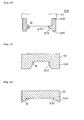
- Fig. 15 and Fig. 16 show the angle of inclination, ⁇ , of the tapered plane 51d of the protruding ridge section 51a in the wafer periphery pressing jigs 50 and 50A - 50E.
- Fig. 15 shows the angle of inclination, ⁇ , of the tapered plane 51d of the type employed in the wafer periphery pressing jig 50, 50A, 50C, and 50D.
- Fig. 16 shows the angle of inclination, ⁇ , of the tapered plane 51d of the type employed in the wafer periphery pressing jig 50B and 50E.
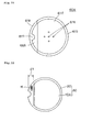
- a specified portion of the bonding wafer 30 subject to the second polishing is the portion in the vicinity of the orientation flat.
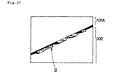
- a width, d, of a terraced section in the vicinity of the orientation flat of the supporting substrate wafer 20 is extended, and the hard laser mark, M, may be printed on that extended terraced section (Fig. 19).
- a partial wafer removing pressing jig 60 is used for partial periphery removing polishing.
- the jig body 61 is made of rigid material, such as PEEK, and has a thick disk-like shape. A top surface of the jig body 61 is affixed with one of the faces of the double-sided tape 52. An annular protruding ridge section 61a is integrally formed with the jig body 61 on a lower surface of a peripheral region thereof. In this configuration, an under surface of the peripheral region of the jig body 61 except a portion located in the vicinity of the orientation flat is securely bonded with an anti-wear frame 61b made of ceramic having generally a C-shape.
- a partial protruding section 62 is formed integrally with the pressing surface 61d in a portion corresponding to that of the orientation flat of the wafer such that the width of the terraced section, d, of the supporting substrate wafer 20 may be extended to 4 mm.
- the partial protruding section 62 is a 0.2 mm high flat raised portion formed adjacently to the orientation flat guide 61c.
- the orientation flat portion of the bonding wafer 30 is deformed by the partial protruding section 62 so as to be protruded more toward the polishing surface side than the central region of the active layer wafer 10, ultimately protruding slightly beyond the lower end face of the protruding ridge section 61a.
- Five pieces of spaced suction ports 61e... are formed in a central region of the pressing surface 61d, which are in communication with an air suction section of a vacuum generator (not shown).
- Fig. 20 through Fig. 22 show an example of a partial wafer removing polishing jig designated generally by reference numeral 60A, which is configured to apply the partial periphery removing polishing to the bonding wafer 30 having a notch.
- a notch guide 61f for guiding the notch portion of the bonding wafer 30 from outside is formed integrally with the protruding ridge section 61a in its portion facing to the notch of the wafer by making this portion thicker into half-moon shape in a bottom view.
- a partial protruding section 62A for extending the width, d1, of the terraced section of the supporting substrate wafer 20 to 4 mm is formed integrally with the pressing surface 61d in its notch portion.
- the description has been provided by taking as an example the bonding SOI substrate that may be fabricated by bonding the active layer wafer and the supporting substrate wafer in one on the other and then reducing the thickness of the active layer wafer through the surface grinding or the like to form the active layer.
- the present invention is not limited to this, but can be applied to the bonding substrate fabricated by, for example, the smart cut method.
- the present invention can be applied also to the bonding substrate fabricated by the ELTRAN method or the SiGen method.
- the periphery removing polishing has been employed as the polishing process subsequent to the surface grinding, in which the defective bonding portion in the peripheral region of the active layer wafer is removed with the central region thereof left un-removed, therefore the periphery grinding of the active layer wafer and the periphery etching of the active layer, which have been required in the prior art, can be eliminated. Owing to this, the number of manufacturing processes of the bonding substrate can be reduced and the manufacturing time of the bonding substrate can also be reduced.
- the bonding wafer can be fabricated without causing any peripheral region of the wafer to be stripped even without applying the thermal processing for enhancing the bonding strength after bonding the active layer wafer and the supporting substrate wafer under a room temperature, by applying the surface grinding to the active layer wafer and also applying the periphery removing polishing to the peripheral region of the active layer.
- the thermal processing is applied in the reducing atmosphere or in the inactive atmosphere after the central region of the active layer has been polished, the crystal defect can be removed from the surface of the active layer even if the thermal processing in the above atmosphere is not applied separately from the bonding thermal processing. It means that the surface of the active layer can be made a defect-free surface.
Landscapes
- Engineering & Computer Science (AREA)
- Mechanical Engineering (AREA)
- Mechanical Treatment Of Semiconductor (AREA)
Applications Claiming Priority (3)
| Application Number | Priority Date | Filing Date | Title |
|---|---|---|---|
| JP2002145327 | 2002-05-20 | ||
| JP2002145327 | 2002-05-20 | ||
| PCT/JP2003/005652 WO2003098695A1 (en) | 2002-05-20 | 2003-05-02 | Laminated substrate, method of manufacturing the substrate, and wafer outer periphery pressing jigs used for the method |
Publications (3)
| Publication Number | Publication Date |
|---|---|
| EP1507292A1 true EP1507292A1 (de) | 2005-02-16 |
| EP1507292A4 EP1507292A4 (de) | 2007-03-28 |
| EP1507292B1 EP1507292B1 (de) | 2012-05-02 |
Family
ID=29545083
Family Applications (1)
| Application Number | Title | Priority Date | Filing Date |
|---|---|---|---|
| EP03721027A Expired - Lifetime EP1507292B1 (de) | 2002-05-20 | 2003-05-02 | Verfahren zur herstellung des laminiertes substrats und für das verfahren benutzte druckeinspannvorrichtungen für die äussere wafer-peripherie |
Country Status (7)
| Country | Link |
|---|---|
| US (1) | US7378332B2 (de) |
| EP (1) | EP1507292B1 (de) |
| JP (1) | JP4281685B2 (de) |
| KR (1) | KR100577627B1 (de) |
| CN (1) | CN1639869B (de) |
| TW (1) | TWI224356B (de) |
| WO (1) | WO2003098695A1 (de) |
Cited By (5)
| Publication number | Priority date | Publication date | Assignee | Title |
|---|---|---|---|---|
| EP2259301A3 (de) * | 2003-10-14 | 2010-12-22 | S.O.I. Tec Silicon on Insulator Technologies | Verfahren zur Vorbereitung und zum Zusammenbau von Substraten |
| EP1887613A4 (de) * | 2005-05-31 | 2011-04-27 | Shinetsu Handotai Kk | Bond-wafer-herstellungsverfahren und vorrichtung zum schleifen des äusseren rands eines bond-wafers |
| US8298916B2 (en) | 2010-03-02 | 2012-10-30 | Soitec | Process for fabricating a multilayer structure with post-grinding trimming |
| US8530331B2 (en) | 2006-04-10 | 2013-09-10 | Commissariat A L'energie Atomique | Process for assembling substrates with low-temperature heat treatments |
| AT14714U1 (de) * | 2010-06-21 | 2016-04-15 | Brewer Science Inc | Verfahren und vorrichtung zur entfernung eines reversibel montierten bausteinwafers von einem trägersubstrat |
Families Citing this family (31)
| Publication number | Priority date | Publication date | Assignee | Title |
|---|---|---|---|---|
| US7919815B1 (en) * | 2005-02-24 | 2011-04-05 | Saint-Gobain Ceramics & Plastics, Inc. | Spinel wafers and methods of preparation |
| JP4604889B2 (ja) * | 2005-05-25 | 2011-01-05 | 株式会社Sumco | シリコンウェーハの製造方法、並びにシリコン単結晶育成方法 |
| US7790565B2 (en) * | 2006-04-21 | 2010-09-07 | Corning Incorporated | Semiconductor on glass insulator made using improved thinning process |
| JP2009176918A (ja) * | 2008-01-24 | 2009-08-06 | Sumco Corp | Soi基板の製造方法 |
| DE112009000140B4 (de) * | 2008-01-24 | 2022-06-15 | Brewer Science, Inc. | Verfahren zum reversiblen Anbringen eines Vorrichtungswafers an einem Trägersubstrat und ein daraus erhaltener Gegenstand |
| JP5564785B2 (ja) * | 2008-12-08 | 2014-08-06 | 株式会社Sumco | 貼り合わせ基板の製造方法 |
| JP2011210821A (ja) * | 2010-03-29 | 2011-10-20 | Renesas Electronics Corp | 半導体装置とその製造方法 |
| US9263314B2 (en) | 2010-08-06 | 2016-02-16 | Brewer Science Inc. | Multiple bonding layers for thin-wafer handling |
| FR2969373B1 (fr) * | 2010-12-20 | 2013-07-19 | St Microelectronics Crolles 2 | Procede d'assemblage de deux plaques et dispositif correspondant |
| KR101570917B1 (ko) | 2011-04-11 | 2015-11-20 | 에베 그룹 에. 탈너 게엠베하 | 가요성의 캐리어 마운트 및 캐리어 기판을 분리하기 위한 장치 및 방법 |
| US10857649B2 (en) * | 2011-09-22 | 2020-12-08 | Taiwan Semiconductor Manufacturing Company, Ltd. | Method and apparatus for performing a polishing process in semiconductor fabrication |
| DE112012004373T5 (de) * | 2011-10-18 | 2014-07-10 | Fuji Electric Co., Ltd | Verfahren zur trennung eines trägersubstrats von einem festphasengebundenen wafer und verfahren zur herstellung einer halbleitervorrichtung |
| KR101544734B1 (ko) * | 2011-11-22 | 2015-08-17 | 다즈모 가부시키가이샤 | 가압원판, 접합장치 및 접합방법 |
| US10643853B2 (en) * | 2012-02-10 | 2020-05-05 | Taiwan Semiconductor Manufacturing Company, Ltd. | Wafer thinning apparatus having feedback control and method of using |
| US8580655B2 (en) | 2012-03-02 | 2013-11-12 | Disco Corporation | Processing method for bump-included device wafer |
| JP5978764B2 (ja) * | 2012-05-24 | 2016-08-24 | 信越半導体株式会社 | Soiウェーハの製造方法 |
| US20140054748A1 (en) * | 2012-08-21 | 2014-02-27 | Genmao Liu | Edge trimming method for semiconductor wafer and semiconductor wafer having trimmed edge |
| TWI470730B (zh) * | 2012-09-18 | 2015-01-21 | Asia Pacific Microsystems Inc | Wafer holding device |
| KR102061695B1 (ko) | 2012-10-17 | 2020-01-02 | 삼성전자주식회사 | 웨이퍼 가공 방법 |
| US9028628B2 (en) | 2013-03-14 | 2015-05-12 | International Business Machines Corporation | Wafer-to-wafer oxide fusion bonding |
| US9058974B2 (en) | 2013-06-03 | 2015-06-16 | International Business Machines Corporation | Distorting donor wafer to corresponding distortion of host wafer |
| JP6230381B2 (ja) * | 2013-11-15 | 2017-11-15 | 株式会社ディスコ | 加工方法 |
| KR20240160250A (ko) * | 2016-09-29 | 2024-11-08 | 에베 그룹 에. 탈너 게엠베하 | 2개의 기판을 접합하기 위한 장치 및 방법 |
| US10553474B1 (en) | 2018-08-29 | 2020-02-04 | Taiwan Semiconductor Manufacturing Co., Ltd. | Method for forming a semiconductor-on-insulator (SOI) substrate |
| JP7339056B2 (ja) | 2019-07-31 | 2023-09-05 | グローバルウェーハズ・ジャパン株式会社 | 貼り合わせウェーハ及びそれを用いた積層ウェーハの製造方法 |
| WO2021199585A1 (ja) * | 2020-04-02 | 2021-10-07 | 東京エレクトロン株式会社 | 基板処理方法及び基板処理装置 |
| CN113211306A (zh) * | 2021-05-28 | 2021-08-06 | 福建晶安光电有限公司 | 一种用于半导体晶片抛光的陶瓷载盘 |
| CN113510609B (zh) * | 2021-07-12 | 2023-09-08 | 长鑫存储技术有限公司 | 晶圆以及晶圆的处理方法 |
| CN115458390B (zh) * | 2022-07-27 | 2024-11-12 | 武汉新芯集成电路股份有限公司 | 三维集成结构及其制作方法 |
| CN115464484B (zh) * | 2022-10-14 | 2024-06-07 | 杭州乾晶半导体有限公司 | 一种碳化硅晶片双面加工方法以及相应的装置 |
| WO2024103220A1 (zh) * | 2022-11-14 | 2024-05-23 | 上海显耀显示科技有限公司 | 一种补偿键合形变量的键合治具 |
Family Cites Families (11)
| Publication number | Priority date | Publication date | Assignee | Title |
|---|---|---|---|---|
| JPH02181469A (ja) | 1989-01-05 | 1990-07-16 | Fujitsu Ltd | 半導体基板の製造方法 |
| JPH0636413B2 (ja) * | 1990-03-29 | 1994-05-11 | 信越半導体株式会社 | 半導体素子形成用基板の製造方法 |
| JP3618105B2 (ja) * | 1991-03-07 | 2005-02-09 | 株式会社日本自動車部品総合研究所 | 半導体基板の製造方法 |
| JPH05109678A (ja) | 1991-10-18 | 1993-04-30 | Sony Corp | Soi基板の製造方法 |
| JPH05226305A (ja) * | 1992-02-10 | 1993-09-03 | Hitachi Ltd | 張合せウェハの製造方法 |
| JP3580600B2 (ja) * | 1995-06-09 | 2004-10-27 | 株式会社ルネサステクノロジ | 半導体装置の製造方法およびそれに使用される半導体ウエハ並びにその製造方法 |
| EP0935280B1 (de) * | 1998-02-04 | 2004-06-09 | Canon Kabushiki Kaisha | SOI Substrat |
| US6287941B1 (en) | 1999-04-21 | 2001-09-11 | Silicon Genesis Corporation | Surface finishing of SOI substrates using an EPI process |
| KR100789205B1 (ko) | 2000-03-29 | 2007-12-31 | 신에쯔 한도타이 가부시키가이샤 | 실리콘 웨이퍼 및 에스오아이 웨이퍼의 제조방법, 그리고그 에스오아이 웨이퍼 |
| US6722964B2 (en) * | 2000-04-04 | 2004-04-20 | Ebara Corporation | Polishing apparatus and method |
| JP2003142439A (ja) | 2001-11-08 | 2003-05-16 | Nikon Corp | ウェハの研磨方法及びマスク |
-
2003
- 2003-05-02 KR KR1020037014758A patent/KR100577627B1/ko not_active Expired - Lifetime
- 2003-05-02 WO PCT/JP2003/005652 patent/WO2003098695A1/ja not_active Ceased
- 2003-05-02 EP EP03721027A patent/EP1507292B1/de not_active Expired - Lifetime
- 2003-05-02 JP JP2004506089A patent/JP4281685B2/ja not_active Expired - Lifetime
- 2003-05-02 CN CN03804904XA patent/CN1639869B/zh not_active Expired - Lifetime
- 2003-05-02 US US10/499,028 patent/US7378332B2/en not_active Expired - Lifetime
- 2003-10-07 TW TW092127765A patent/TWI224356B/zh not_active IP Right Cessation
Cited By (5)
| Publication number | Priority date | Publication date | Assignee | Title |
|---|---|---|---|---|
| EP2259301A3 (de) * | 2003-10-14 | 2010-12-22 | S.O.I. Tec Silicon on Insulator Technologies | Verfahren zur Vorbereitung und zum Zusammenbau von Substraten |
| EP1887613A4 (de) * | 2005-05-31 | 2011-04-27 | Shinetsu Handotai Kk | Bond-wafer-herstellungsverfahren und vorrichtung zum schleifen des äusseren rands eines bond-wafers |
| US8530331B2 (en) | 2006-04-10 | 2013-09-10 | Commissariat A L'energie Atomique | Process for assembling substrates with low-temperature heat treatments |
| US8298916B2 (en) | 2010-03-02 | 2012-10-30 | Soitec | Process for fabricating a multilayer structure with post-grinding trimming |
| AT14714U1 (de) * | 2010-06-21 | 2016-04-15 | Brewer Science Inc | Verfahren und vorrichtung zur entfernung eines reversibel montierten bausteinwafers von einem trägersubstrat |
Also Published As
| Publication number | Publication date |
|---|---|
| KR100577627B1 (ko) | 2006-05-10 |
| US7378332B2 (en) | 2008-05-27 |
| EP1507292B1 (de) | 2012-05-02 |
| US20050014347A1 (en) | 2005-01-20 |
| JPWO2003098695A1 (ja) | 2005-09-22 |
| JP4281685B2 (ja) | 2009-06-17 |
| CN1639869A (zh) | 2005-07-13 |
| WO2003098695A1 (en) | 2003-11-27 |
| TWI224356B (en) | 2004-11-21 |
| KR20040028757A (ko) | 2004-04-03 |
| EP1507292A4 (de) | 2007-03-28 |
| CN1639869B (zh) | 2010-05-26 |
| TW200425222A (en) | 2004-11-16 |
Similar Documents
| Publication | Publication Date | Title |
|---|---|---|
| EP1507292B1 (de) | Verfahren zur herstellung des laminiertes substrats und für das verfahren benutzte druckeinspannvorrichtungen für die äussere wafer-peripherie | |
| US7855129B2 (en) | Method for manufacturing direct bonded SOI wafer and direct bonded SOI wafer manufactured by the method | |
| EP1962325B1 (de) | Verfahren zur herstellung eines gebondeten substrats | |
| EP1189266B1 (de) | Methode zur herstellung einer siliziumhalbleiterscheibe und einer soi-scheibe soiwe soi-scheibe | |
| US20030008478A1 (en) | Production method for silicon wafer and soi wafer, and soi wafer | |
| WO2003094215A1 (en) | Semiconductor wafer manufacturing method and wafer | |
| EP1887613A1 (de) | Bond-wafer-herstellungsverfahren und vorrichtung zum schleifen des äusseren rands eines bond-wafers | |
| JP2006222453A (ja) | シリコンウエーハの製造方法及びシリコンウエーハ並びにsoiウエーハ | |
| JP4398934B2 (ja) | Soiウエーハの製造方法 | |
| JP2662495B2 (ja) | 接着半導体基板の製造方法 | |
| US20070148917A1 (en) | Process for Regeneration of a Layer Transferred Wafer and Regenerated Layer Transferred Wafer | |
| JP4224871B2 (ja) | 半導体基板の製造方法 | |
| JP4103808B2 (ja) | ウエーハの研削方法及びウエーハ | |
| JP4232148B2 (ja) | 貼り合わせ基板の製造方法 | |
| JP3978780B2 (ja) | ウエーハの研磨方法及び装置 | |
| JP2004022838A (ja) | 貼り合わせsoi基板およびその製造方法 | |
| JPH1187203A (ja) | 基板の貼り合わせ方法 | |
| JP2002043255A (ja) | シリコンエピタキシャルウェーハの製造方法 | |
| JP2011091143A (ja) | シリコンエピタキシャルウェーハの製造方法 | |
| JP2005079109A (ja) | 貼合せsoiウェーハの製造方法及び該方法により製造された貼合せsoiウェーハ | |
| JP2001313380A (ja) | 張り合わせ基板およびその製造方法 | |
| JPH1126337A (ja) | 貼り合わせ基板の作製方法 | |
| JP2002353176A (ja) | シリコンエピタキシャルウェーハの製造方法 | |
| JPH11340443A (ja) | Soiウエーハの作製方法およびsoiウエーハ | |
| KR20110037662A (ko) | 템플레이트 어셈블리 및 그 제조방법 |
Legal Events
| Date | Code | Title | Description |
|---|---|---|---|
| PUAI | Public reference made under article 153(3) epc to a published international application that has entered the european phase |
Free format text: ORIGINAL CODE: 0009012 |
|
| 17P | Request for examination filed |
Effective date: 20040302 |
|
| AK | Designated contracting states |
Kind code of ref document: A1 Designated state(s): AT BE BG CH CY CZ DE DK EE ES FI FR GB GR HU IE IT LI LU MC NL PT RO SE SI SK TR |
|
| RBV | Designated contracting states (corrected) |
Designated state(s): AT BE BG DE FR IT |
|
| RAP1 | Party data changed (applicant data changed or rights of an application transferred) |
Owner name: SUMCO CORPORATION |
|
| A4 | Supplementary search report drawn up and despatched |
Effective date: 20070223 |
|
| RIC1 | Information provided on ipc code assigned before grant |
Ipc: H01L 21/762 20060101AFI20070219BHEP |
|
| 17Q | First examination report despatched |
Effective date: 20080311 |
|
| RTI1 | Title (correction) |
Free format text: METHOD OF MANUFACTURING THE SUBSTRATE, AND WAFER OUTER PERIPHERY PRESSING JIGS USED FOR THE METHOD |
|
| GRAP | Despatch of communication of intention to grant a patent |
Free format text: ORIGINAL CODE: EPIDOSNIGR1 |
|
| GRAS | Grant fee paid |
Free format text: ORIGINAL CODE: EPIDOSNIGR3 |
|
| GRAA | (expected) grant |
Free format text: ORIGINAL CODE: 0009210 |
|
| AK | Designated contracting states |
Kind code of ref document: B1 Designated state(s): DE FR IT |
|
| RBV | Designated contracting states (corrected) |
Designated state(s): DE FR IT |
|
| REG | Reference to a national code |
Ref country code: DE Ref legal event code: R096 Ref document number: 60340805 Country of ref document: DE Effective date: 20120628 |
|
| PLBE | No opposition filed within time limit |
Free format text: ORIGINAL CODE: 0009261 |
|
| STAA | Information on the status of an ep patent application or granted ep patent |
Free format text: STATUS: NO OPPOSITION FILED WITHIN TIME LIMIT |
|
| 26N | No opposition filed |
Effective date: 20130205 |
|
| REG | Reference to a national code |
Ref country code: DE Ref legal event code: R097 Ref document number: 60340805 Country of ref document: DE Effective date: 20130205 |
|
| REG | Reference to a national code |
Ref country code: FR Ref legal event code: PLFP Year of fee payment: 13 |
|
| REG | Reference to a national code |
Ref country code: FR Ref legal event code: PLFP Year of fee payment: 14 |
|
| REG | Reference to a national code |
Ref country code: DE Ref legal event code: R082 Ref document number: 60340805 Country of ref document: DE Representative=s name: GLAWE DELFS MOLL PARTNERSCHAFT MBB VON PATENT-, DE |
|
| REG | Reference to a national code |
Ref country code: FR Ref legal event code: PLFP Year of fee payment: 15 |
|
| REG | Reference to a national code |
Ref country code: FR Ref legal event code: PLFP Year of fee payment: 16 |
|
| PGFP | Annual fee paid to national office [announced via postgrant information from national office to epo] |
Ref country code: IT Payment date: 20220524 Year of fee payment: 20 Ref country code: FR Payment date: 20220523 Year of fee payment: 20 Ref country code: DE Payment date: 20220519 Year of fee payment: 20 |
|
| REG | Reference to a national code |
Ref country code: DE Ref legal event code: R071 Ref document number: 60340805 Country of ref document: DE |