EP1513199A2 - Festkörperbildaufnahmevorrichtung und Kamera - Google Patents
Festkörperbildaufnahmevorrichtung und Kamera Download PDFInfo
- Publication number
- EP1513199A2 EP1513199A2 EP04020721A EP04020721A EP1513199A2 EP 1513199 A2 EP1513199 A2 EP 1513199A2 EP 04020721 A EP04020721 A EP 04020721A EP 04020721 A EP04020721 A EP 04020721A EP 1513199 A2 EP1513199 A2 EP 1513199A2
- Authority
- EP
- European Patent Office
- Prior art keywords
- region
- depth
- solid
- state imaging
- device isolation
- Prior art date
- Legal status (The legal status is an assumption and is not a legal conclusion. Google has not performed a legal analysis and makes no representation as to the accuracy of the status listed.)
- Withdrawn
Links
Images


Classifications
-
- H—ELECTRICITY
- H10—SEMICONDUCTOR DEVICES; ELECTRIC SOLID-STATE DEVICES NOT OTHERWISE PROVIDED FOR
- H10F—INORGANIC SEMICONDUCTOR DEVICES SENSITIVE TO INFRARED RADIATION, LIGHT, ELECTROMAGNETIC RADIATION OF SHORTER WAVELENGTH OR CORPUSCULAR RADIATION
- H10F99/00—Subject matter not provided for in other groups of this subclass
-
- H—ELECTRICITY
- H10—SEMICONDUCTOR DEVICES; ELECTRIC SOLID-STATE DEVICES NOT OTHERWISE PROVIDED FOR
- H10F—INORGANIC SEMICONDUCTOR DEVICES SENSITIVE TO INFRARED RADIATION, LIGHT, ELECTROMAGNETIC RADIATION OF SHORTER WAVELENGTH OR CORPUSCULAR RADIATION
- H10F39/00—Integrated devices, or assemblies of multiple devices, comprising at least one element covered by group H10F30/00, e.g. radiation detectors comprising photodiode arrays
- H10F39/80—Constructional details of image sensors
-
- H—ELECTRICITY
- H10—SEMICONDUCTOR DEVICES; ELECTRIC SOLID-STATE DEVICES NOT OTHERWISE PROVIDED FOR
- H10F—INORGANIC SEMICONDUCTOR DEVICES SENSITIVE TO INFRARED RADIATION, LIGHT, ELECTROMAGNETIC RADIATION OF SHORTER WAVELENGTH OR CORPUSCULAR RADIATION
- H10F30/00—Individual radiation-sensitive semiconductor devices in which radiation controls the flow of current through the devices, e.g. photodetectors
- H10F30/20—Individual radiation-sensitive semiconductor devices in which radiation controls the flow of current through the devices, e.g. photodetectors the devices having potential barriers, e.g. phototransistors
-
- H—ELECTRICITY
- H10—SEMICONDUCTOR DEVICES; ELECTRIC SOLID-STATE DEVICES NOT OTHERWISE PROVIDED FOR
- H10F—INORGANIC SEMICONDUCTOR DEVICES SENSITIVE TO INFRARED RADIATION, LIGHT, ELECTROMAGNETIC RADIATION OF SHORTER WAVELENGTH OR CORPUSCULAR RADIATION
- H10F39/00—Integrated devices, or assemblies of multiple devices, comprising at least one element covered by group H10F30/00, e.g. radiation detectors comprising photodiode arrays
- H10F39/80—Constructional details of image sensors
- H10F39/803—Pixels having integrated switching, control, storage or amplification elements
-
- H—ELECTRICITY
- H10—SEMICONDUCTOR DEVICES; ELECTRIC SOLID-STATE DEVICES NOT OTHERWISE PROVIDED FOR
- H10F—INORGANIC SEMICONDUCTOR DEVICES SENSITIVE TO INFRARED RADIATION, LIGHT, ELECTROMAGNETIC RADIATION OF SHORTER WAVELENGTH OR CORPUSCULAR RADIATION
- H10F39/00—Integrated devices, or assemblies of multiple devices, comprising at least one element covered by group H10F30/00, e.g. radiation detectors comprising photodiode arrays
- H10F39/80—Constructional details of image sensors
- H10F39/807—Pixel isolation structures
Definitions
- the present invention relates to a MOS type solid-state imaging device intended for a digital camera.
- Metal-Oxide-Semiconductor (MOS) type solid-state imaging device is an image sensor that amplifies and reads out each signal of the photon electric charge accumulated in a photodiode within each pixel, using an amplifier circuit that includes an insulated gate field effect transistor formed in each pixel (to be referred to as "MOS transistor” hereinafter).
- MOS transistor insulated gate field effect transistor formed in each pixel
- a Complementary MOS (CMOS) image sensor manufactured in the CMOS process draws attention as an image input device for a portable device such as a small camera for Personal Computer (PC).
- PC Personal Computer
- Fig. 1 is a cross-sectional view showing an example of the structure of an N-channel MOS transistor composing an imaging region of the conventional MOS type solid-state imaging device and a trench isolation unit.
- a P type well region is formed on a silicon substrate 8.
- the N-channel MOS transistor is formed and a source region of the N-channel MOS transistor forms a part of the photodiode 10.
- photons are converted into electric charge (i.e., electric charge is generated by exposure to light).
- an oxide film formed by LOCal Oxidation of Silicon (LOCOS) is used for the trench isolation unit which isolates the neighboring elements (e.g., MOS transistors).
- the oxide film formed by Shallow Trench Isolation (STI) is used for the device isolation region, as can be seen in the trench isolation unit 9 shown in Fig. 1.
- STI Shallow Trench Isolation
- Fig. 2 is a diagram showing an example of the structure of the conventional MOS type solid-state imaging device.
- the MOS type solid-state imaging device is comprised of the following: an imaging region 27 where plural pixels 26 are two-dimensionally arranged on the silicon substrate 8; a vertical shift transistor 28 and a horizontal shift transistor 29 for selecting pixels; and a timing generation circuit 30 for providing pulses necessary for the shift registers.
- Each pixel 26 in the imaging region 27 is composed of a photoelectric conversion unit 31 and four MOS transistors of a transfer transistor 32, a reset transistor 23, an amplifier transistor 24, and a select transistor 25.
- a film stress due to a nitride film or the like, an ion implantation or an etching process causes defects in the MOS type solid-state imaging device formed by using the LOCOS or the STI for the device isolation region.
- the defects cause dark currents or white flaws.
- the use of the LOCOS causes difficulty in the miniaturization of the imaging region 27 because a bird's beak width gets longer.
- the use of the STI causes a problem that the stress is generated due to an embedded oxide film.
- Figs 3A-3F respectively shows a cross-sectional view showing how the device isolation region according to the MOS type solid-state imaging device in the conventional example 1 is built during the manufacturing process.
- a SiO 2 film is deposited on the semiconductor substrate 61 as a gate dielectric film 52 by means of thermal oxidation so that the thickness of the film becomes 0.1 ⁇ m. Then, a channel stopper 53, a photoelectric conversion unit 54 and a drain 55 are formed by performing ion implantation via the gate dielectric film (thermal oxide film) 52. As shown in Fig. 3B, a CVD oxide film 56 is then deposited on the gate dielectric film so that the thickness becomes approximately 0.3 ⁇ m. After the deposit of the CVD oxide film (resist) 56, etching is performed on the CVD oxide film 56 and the gate oxide film 52 based on an RIE method using a mask so that a gate channel 57 is opened.
- a gate oxide film is then formed in the channel region by performing oxidation again after having deposited a gate electrode 58 made of polysilicon.
- a polysilicon wiring pattern is formed by performing, using a resist mask, the RIE on the gate electrode 58 with the pattern larger at least than the gate channel 57.
- an interlayer dielectric 59 made of SiO 2 and others is deposited and then is partly opened using the RIE method so that the dielectric film 59 is conducted with the drain 55 and a signal line 60 is embedded.
- the MOS type solid-state imaging device has an amplifier circuit in each pixel, and is characterized in that a high sensitivity can be realized by amplifying small electric signals. Therefore, in the case where the amount of the leak current leaking into the photodiode is large, the leak current is also amplified and big noises are caused. Due to the noises, the deterioration of the image is a crucial issue.
- the leak current means all the currents that leak into the photodiode apart form the current generated by converting photons into electric charge in the photodiode.
- the degradation of the sensitivity due to the decrease in the surface of the imaging region is a problem specific to the miniaturization as described above.
- the sensitivity in the photodiode region indicates the smallest quantity of photon electric charge in which an amount of photoelectric converted charge surpasses an amount of noise charge caused by the leak current.
- the decrease in the amount of noise electric charge is indispensable for improving the sensitivity.
- the miniaturized MOS transistor has been developed utilizing miniaturization technology for semiconductor LSI, and the reality is that no attention is paid to the leak current.
- the STI which is already explained as a device isolation structure suitable for the miniaturization of the solid-state imaging device is widely used for the semiconductor devices.
- the STI due to its structure in which a trench is formed in a silicon substrate by performing dry etching and the trench is filled with an oxide film, a strong stress is caused within the silicon substrate because of the difference in thermal expansion coefficient between the filled oxide film and the silicon substrate. The stress concentrates on the corner of the bottom part of the trench for its steep angles. The existence of the stress that is resistant to crystals increases the density of crystal defect for stabilizing crystal energy.
- the electron generated due to the crystal defect is one of the causes of the leak current.
- the interface state that is not involved in bonding is formed as the interface between the silicon substrate and the embedded oxide film where non-bonding electrons exist.
- the crystal structure on or in the vicinity of the interface between the silicon substrate and the embedded oxide film is extremely disordered since the trench isolation unit is formed by means of dry etching. This is why many non-bonding electrons that are not involved in bonding are found on or in the vicinity of the interface (the non-bonding electrons on and in the vicinity of the interface is termed "interface state leak"). A large leak current is caused by this interface state leak.
- the solid-state imaging device having the MOS transistor miniaturized by the semiconductor LSI technique faces a problem that the leak current caused by the crystal defect induced by the stress and the leak current generated from the interface state with the STI which includes the silicon surface cause much larger noises.
- the device isolation region is formed by means of channel stop implanting. It is necessary to widen the region width of the device isolation region in order to retain enough withstanding pressure in the device isolation region.
- the present invention is conceived in view of the above problems, and an object of the present invention is to provide the MOS type solid-state imaging device that can easily realize the miniaturization of the imaging region and the retaining of the withstanding pressure in the device isolation region.
- the solid-sate imaging device is a solid-state imaging device comprising, for each pixel, an imaging region including: a photodiode having a charge accumulation region of a first conductivity type; and a transistor for reading out the charge obtained by the photodiode, wherein the imaging region includes a device isolation region for isolating said transistor from a neighboring transistor that is placed outside said imaging region, and a depth of the device isolation region is less than a depth of the charge accumulation region, the depth of said region being a depth at which impurity density of said region is at maximum.
- the depth of the device isolation region made less than the depth of the charge accumulation region at which the impurity density is at maximum, the stress imposed on the photodiode is greatly reduced. As a result, it is possible to reduce the amount of leak current because the generation of crystal defect is suppressed in the photodiode.
- the result can be applied both to the device isolation region based on the STI and the one based on the LOCOS.
- the MOS transistors are N-channel type MOS transistors, however, they may be P-channel type MOS transistors instead.
- the MOS transistor has a structure in which the source and the drain which make up a P type diffusion region are formed in the N type semiconductor substrate (or an N type well).
- the transistors composing a circuit other than the imaging region may be CMOS transistors.
- the present invention characterized in that the solid-state imaging device is used for a camera.
- the solid-state imaging device By suppressing the amount of dark current using the method described above, the solid-state imaging device with extremely small noises can be manufactured. It is therefore possible to realize the camera that can function under the condition of low-light intensity.
- MOS type solid-state imaging device With the MOS type solid-state imaging device according to the present invention, it is possible to reduce the noises due to leak current by rendering the structure of the device isolation region specific placed between the MOS transistors. Therefore, the practical value is very high.
- Fig. 4 is a cross-sectional view showing the structure of the N-channel MOS transistor used for the imaging region and the structure of the trench isolation unit in the MOS type solid-state imaging device 110 according to the present embodiment.
- the MOS transistor is isolated from a neighboring MOS transistor by a device isolation region 2.
- a photodiode 3 is formed as an N type diffusion region within the silicon substrate (or a P type well) 1.
- the photodiode 3 serves also as the source of the MOS transistor in the imaging region, and the device isolation region 2 is formed in the region adjoining the photodiode 3, as is the case of other MOS transistors.
- a P type diffusion region is formed as a dark-current suppression layer 6 in the periphery of the surface of the N type diffusion region being the photodiode 3.
- the dark-current suppression layer 6 extends, as shown in Fig. 4, to the periphery of the device isolation region 2. It is also preferable that the dark-current suppression layer 6 is formed in the position ranging from 10 to 200 nm below the surface of the silicon substrate 1. In order to improve the sensitivity, it is desirable that the dark-current suppression layer 6 is formed in the position ranging from 10 to 100 nm below the surface of the silicon substrate 1.
- the device isolation region 2 is formed using a dry etching method, and the depth ranges from 1 to 200 nm that is shallower than that of the dark-current suppression layer 6.
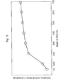
- Fig. 5 is a diagram showing the relationship between an average value of the vertical stresses that remain in the boundary between the photodiode and the dark-current suppression layer, and the depth of the device isolation region 2. It should be noted that the depth of the device isolation region 2 ranges from 50 to 700 nm.
- the average value of the stresses is a value obtained as a result of logic calculation made in an elastic flow model. As shown in Fig. 5, when the depth of the device isolation region 2 ranges from 200 to 700 nm, the average value of the stresses indicates a rather great value and does not virtually depend on the depth of the device isolation region 2. However, it is assumed that the depth of the boundary between the photodiode and the dark-current suppression layer 6 is 200 nm. Fig. 5 also indicates that the remaining vertical stresses of the photodiode suddenly decrease when the depth of the device isolation region 2 is shallower. This attributes greatly to the decrease in a depth-width ratio of the device isolation region 2 in addition to the increasing distance between the device isolation region 2 and the boundary between the photodiode and the dark-current suppression layer 6.
- the depth of the device isolation region within the range of 1 to 100 nm in order to reduce the amount of leak current.
- Fig. 6 is a diagram showing the impurity density profile in the cross-section vertical to the silicon substrate surface on the photodiode.
- a vertical axis indicates impurity density whereas a horizontal axis indicates a depth measured from the silicon substrate surface.
- the impurity density profile shown in Fig. 6 shows a suitable distribution which allows a highly efficient accumulation of the photon electric charge on the photodiode and an effective read transfer.
- the impurity density profile shows two density maxima: the less steep one indicates the dark-current suppression layer, and the depth at which the density is at maximum is approximately 100 nm; and the steeper one indicates the photodiode, and the depth at which the density is at maximum ranges from 150 to 200 nm.
- the depth of the device isolation region measured from the surface of the silicon substrate is set as 150 nm or below.
- the depth of the dark-current suppression layer (i.e., the depth of the boundary between the photodiode and the dark-current suppression layer measured from the surface of the silicon substrate) should be 200 nm or below in order to suppress light absorption by the dark-current suppression unit so as to prevent the decrease in the sensitivity. It is preferable that the depth of the dark-current suppression layer ranges from 10 to 100 nm. As shown in Fig. 6, in the profile of implanted impurity density within the silicon substrate for the optimized photodiode and the dark-current suppression layer, the impurity density of the boundary between the dark-current suppression layer and the photodiode is approximately 100 nm from the surface of the silicon substrate.
- the depth of the maximum density for the impurities in the dark-current suppression layer is approximately 50 nm.
- a diffusion activation energy of recombined electrons generated at the boundary between the device isolation region and the silicon substrate increases greatly in the photodiode direction.
- the device isolation region 2 shown in Fig. 4 is formed based on the STI, however, the formation may be based on the LOCOS instead.
- the present invention is particularly effective in the case where the device isolation region 2 is formed based on the STI. The following explains the reasons.
- Fig. 7 is a diagram showing the part on which the stress concentrates at the bottom of the STI.
- the device isolation based on the LOCOS or the STI is conceivable for the device isolation region 2.
- a large amount of leak current are generated in the region, within the semiconductor, which adjoins the corner of the bottom of the STI. This is due to the concentration of stress in the corner of the bottom of the STI. Therefore, the amount of the leak current that leaks into the surface of the photodiode varies greatly depending on the position in depth direction of the bottom of the STI.
- the amount of the leak current that leaks into the photodiode greatly changes according to the four positions in depth direction at the bottom of the STI: the depth of the photodiode; the depth of the photodiode at its maximum density; the depth of the dark-current suppression layer placed in the upper part of the photodiode; and the depth of the dark-current suppression layer at its maximum density.
- the MOS transistor exemplified in the above description is an N-channel type MOS transistor, but it may be a P-channel type MOS transistor for composing the MOS type solid-state imaging device.
- the MOS transistor has a structure in which the source and the drain being a P type diffusion region are formed within the N type semiconductor substrate (or N type well).
- the photodiode is composed of the P type diffusion region while the dark-current suppression layer is composed of the N type diffusion region.
- the circuit for driving the imaging region in the solid-state imaging device includes plural MOS transistors and these MOS transistors are isolated by the device isolation region.
- the same structure as that of the trench isolation unit can be used. Namely, the depth of the trench ranges from 1 to 200 nm, either as same as that of the dark-current suppression layer or below.
- all the MOS transistors composing the imaging region and the periphery drive circuit are either N-channel type MOS transistors or P-channel type MOS transistors. Particularly considering the fact that a high-speed operation can be achieved in the drive circuit, it is preferable that all the MOS transistors are N-channel type MOS transistors.
- the following explains the reason why the solid-state imaging device composed of the MOS transistors of the same conductivity type which make up the drive circuit is more preferable than the solid-state imaging device composed of the CMOS type drive circuit.
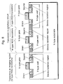
- Fig. 8 is a cross-sectional view of the transistor in the imaging region and the transistor in the periphery circuit region.
- the transistors in the imaging region are N type transistors whereas the transistors in the periphery circuit region are N type transistors and P type transistors.
- the negative effect is that the function of the device isolation region to isolate the N type transistors and the P type transistors may go down.
- the elements may be deconstructed because of the current that flows, though it should not, between the N type transistors and the P type transistors due to a latch-up phenomena.
- Fig. 9 is a cross-sectional view of the solid-state imaging device in the case where the periphery circuit is formed only of N type MOS transistors. It is possible to eliminate the negative effects that appear in the case where the device isolation region is made shallower, by forming the periphery circuit only of the N type transistors so that the latch-up phenomena generated in the case of CMOS type solid-state imaging device can be eliminated. Thus, the solid-state imaging device without the negative effects can be realized by using only the N type transistors for the transistors in the imaging region and those in the periphery circuit in the N type MOS solid-state imaging device.
- Figs 8 and 9 respectively show the case where the transistors in the imaging region are N type transistors.
- the transistors in the imaging region are P type transistors
- the solid-state imaging device without negative effects can be realized by using only the P type transistors for the transistors in the imaging region and those in the periphery circuit in the P type solid-state imaging device.
- the imaging region and the periphery circuit are respectively made up of multiple MOS transistors that are isolated by the device isolation region.
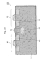
- Fig. 10 shows the structure of the device isolation region between the MOS transistors in the imaging region or in the periphery circuit.
- the diagram is also a cross-sectional view showing how the transistors 40 and 41 are isolated by the device isolation region 42.
- the leak current is generated between the activation region in the transistor 40 and the activation region 44 in the transistor 40 by setting the depth to be ranged from 1 to 200 nm by which the device isolation region 42 erodes the silicon substrate 1.
- the impurity diffusion layer 45 that suppresses the amount of leak current By placing the impurity diffusion layer 45 that suppresses the amount of leak current to the position that is straightly below the device isolation region 42, as shown in Fig. 10, it is possible to suppress the amount of leak current between the transistors as the withstanding pressure relating to the leak current between the transistors isolated by the device isolation region 42 rises.
- Fig. 11 is an example showing the structure of the device isolation region between the MOS transistors in the imaging region or in the periphery circuit within the MOS type solid-state imaging device according to the third embodiment.
- the diagram is also a cross-sectional view showing how the transistors 46 and 47 are isolated by the device isolation region 48.
- the state of the crystal structure at the boundary between the device isolation region 48 and the silicon substrate 1 is so disordered that the leak current is generated. Therefore, it is possible to suppress the interface state leak between the device isolation region 48 and the silicon substrate 1 by forming, on the side of the silicon substrate 1, the impurity diffusion layer 51 along the interface between the side wall of the device isolation region and the silicon substrate 1.
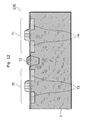
- Fig. 12 is an example of the structure of the MOS transistor in the imaging region or the periphery circuit and the device isolation region within the MOS type solid-state imaging device according to the fourth embodiment.
- the diagram is also a cross-sectional view showing how the transistors 70 and 71 are isolated by the device isolation region 72.
- the depth of the device isolation region 72 measured from the surface of the silicon substrate 1 is deeper than the depth of the activation regions 73 and 74.
- a spatial distance between the activation regions 73 and 74 increases and the leak current between them can be reduced.
- Either of the following isolation structures can be applied to the device isolation region 72: an STI structure in which a trench is formed in the silicon substrate 1 and is embedded using a silicon oxide; and a LOCOS structure using the silicon thermal oxide film generated by directly performing thermal oxidation on the silicon substrate 1 using a selective thermal oxidation process.
- the MOS type solid-state imaging device that causes small noises can be realized with whichever device isolation structure.
- Fig. 13 is a functional block diagram of the camera on which any of the solid-state imaging device having the device isolation structure according to the above embodiments is mounted.
- the camera 200 is comprised of a lens 104, a solid-state imaging device 100, a drive circuit 101, a signal processing unit 102 and an external interface unit 103.
- the light that passes through the lens 104 enters the solid-state imaging device 100.
- the signal processing unit 102 drives the solid-state imaging device 100 through the drive circuit 101 and takes in the output signal from the solid-state imaging device 100.
- the signal processed by the signal processing unit 102 is outputted outside via the external interface unit 103.
- the camera 200 can function without light as it offers high quality for pictures and the sensitivity gets higher.
- the solid-state imaging device according to the present invention is effective enough to easily realize the miniaturization of the imaging region, the retaining of the withstanding pressure in the device isolation region and the reduction in the amount of dark current as well as white flaws. It is therefore useful as the MOS type solid-state imaging device intended for a digital camera or the like.
Landscapes
- Solid State Image Pick-Up Elements (AREA)
- Element Separation (AREA)
Applications Claiming Priority (2)
| Application Number | Priority Date | Filing Date | Title |
|---|---|---|---|
| JP2003311952 | 2003-09-03 | ||
| JP2003311952 | 2003-09-03 |
Publications (2)
| Publication Number | Publication Date |
|---|---|
| EP1513199A2 true EP1513199A2 (de) | 2005-03-09 |
| EP1513199A3 EP1513199A3 (de) | 2006-09-27 |
Family
ID=34131850
Family Applications (1)
| Application Number | Title | Priority Date | Filing Date |
|---|---|---|---|
| EP04020721A Withdrawn EP1513199A3 (de) | 2003-09-03 | 2004-09-01 | Festkörperbildaufnahmevorrichtung und Kamera |
Country Status (5)
| Country | Link |
|---|---|
| US (2) | US7199411B2 (de) |
| EP (1) | EP1513199A3 (de) |
| KR (1) | KR20050025073A (de) |
| CN (2) | CN100472789C (de) |
| TW (1) | TW200518329A (de) |
Families Citing this family (13)
| Publication number | Priority date | Publication date | Assignee | Title |
|---|---|---|---|---|
| US7531405B2 (en) * | 2005-02-28 | 2009-05-12 | Qimonds Ag | Method of manufacturing a dielectric layer and corresponding semiconductor device |
| CN100565892C (zh) * | 2005-04-29 | 2009-12-02 | 皇家飞利浦电子股份有限公司 | 具有图像传感器的半导体器件和这种器件的制造方法 |
| JP2006344644A (ja) * | 2005-06-07 | 2006-12-21 | Matsushita Electric Ind Co Ltd | 固体撮像装置およびカメラならびに固体撮像装置の製造方法 |
| US20060289777A1 (en) * | 2005-06-29 | 2006-12-28 | Wen Li | Detector with electrically isolated pixels |
| US7321141B2 (en) * | 2006-04-18 | 2008-01-22 | United Microelectronics Corp. | Image sensor device and manufacturing method thereof |
| KR100936105B1 (ko) * | 2007-12-28 | 2010-01-11 | 주식회사 동부하이텍 | 이미지센서 및 그 제조방법 |
| JP4759590B2 (ja) | 2008-05-09 | 2011-08-31 | キヤノン株式会社 | 光電変換装置及びそれを用いた撮像システム |
| JP5374941B2 (ja) * | 2008-07-02 | 2013-12-25 | ソニー株式会社 | 固体撮像装置及び電子機器 |
| US8815634B2 (en) * | 2008-10-31 | 2014-08-26 | Varian Semiconductor Equipment Associates, Inc. | Dark currents and reducing defects in image sensors and photovoltaic junctions |
| JP2010212319A (ja) * | 2009-03-09 | 2010-09-24 | Sony Corp | 固体撮像装置、電子機器および固体撮像装置の製造方法 |
| JP2013131516A (ja) * | 2011-12-20 | 2013-07-04 | Sony Corp | 固体撮像装置、固体撮像装置の製造方法、及び、電子機器 |
| JP6579774B2 (ja) * | 2015-03-30 | 2019-09-25 | キヤノン株式会社 | 固体撮像装置およびカメラ |
| EP3324055B1 (de) | 2016-11-21 | 2019-07-03 | Airbus Operations GmbH | Hydraulischer aktuator |
Family Cites Families (14)
| Publication number | Priority date | Publication date | Assignee | Title |
|---|---|---|---|---|
| JP2848268B2 (ja) * | 1995-04-20 | 1999-01-20 | 日本電気株式会社 | 固体撮像装置およびその製造方法 |
| WO1997007629A1 (en) * | 1995-08-11 | 1997-02-27 | Kabushiki Kaisha Toshiba | Mos solid-state image pickup device |
| JP3455655B2 (ja) * | 1997-03-03 | 2003-10-14 | 株式会社東芝 | 固体撮像装置および固体撮像装置応用システム |
| US6690423B1 (en) * | 1998-03-19 | 2004-02-10 | Kabushiki Kaisha Toshiba | Solid-state image pickup apparatus |
| JP2000196057A (ja) | 1998-12-28 | 2000-07-14 | Toshiba Corp | 固体撮像素子およびその製造方法 |
| JP3688980B2 (ja) | 2000-06-28 | 2005-08-31 | 株式会社東芝 | Mos型固体撮像装置及びその製造方法 |
| JP2002314063A (ja) * | 2001-02-06 | 2002-10-25 | Mitsubishi Electric Corp | Cmosイメージセンサ及びその製造方法 |
| JP2003258231A (ja) * | 2002-03-05 | 2003-09-12 | Sony Corp | 固体撮像素子 |
| KR20040008912A (ko) * | 2002-07-19 | 2004-01-31 | 주식회사 하이닉스반도체 | 이미지센서의 하이브리드 소자분리 방법 |
| KR100508086B1 (ko) * | 2002-09-11 | 2005-08-17 | 삼성전자주식회사 | 씨모스 이미지 센서 및 그 제조방법 |
| US7091536B2 (en) * | 2002-11-14 | 2006-08-15 | Micron Technology, Inc. | Isolation process and structure for CMOS imagers |
| JP3621400B2 (ja) | 2003-03-03 | 2005-02-16 | 松下電器産業株式会社 | 固体撮像装置およびその製造方法 |
| US7122408B2 (en) * | 2003-06-16 | 2006-10-17 | Micron Technology, Inc. | Photodiode with ultra-shallow junction for high quantum efficiency CMOS image sensor and method of formation |
| US6900484B2 (en) * | 2003-07-30 | 2005-05-31 | Micron Technology, Inc. | Angled pinned photodiode for high quantum efficiency |
-
2004
- 2004-09-01 EP EP04020721A patent/EP1513199A3/de not_active Withdrawn
- 2004-09-01 US US10/930,814 patent/US7199411B2/en not_active Expired - Lifetime
- 2004-09-02 TW TW093126500A patent/TW200518329A/zh unknown
- 2004-09-03 CN CNB2004100752086A patent/CN100472789C/zh not_active Expired - Lifetime
- 2004-09-03 CN CNA2008101738169A patent/CN101399281A/zh active Pending
- 2004-09-03 KR KR1020040070404A patent/KR20050025073A/ko not_active Withdrawn
-
2006
- 2006-09-20 US US11/523,578 patent/US20070012968A1/en not_active Abandoned
Also Published As
| Publication number | Publication date |
|---|---|
| US20070012968A1 (en) | 2007-01-18 |
| CN101399281A (zh) | 2009-04-01 |
| EP1513199A3 (de) | 2006-09-27 |
| US20050045925A1 (en) | 2005-03-03 |
| TW200518329A (en) | 2005-06-01 |
| KR20050025073A (ko) | 2005-03-11 |
| US7199411B2 (en) | 2007-04-03 |
| CN1591888A (zh) | 2005-03-09 |
| CN100472789C (zh) | 2009-03-25 |
Similar Documents
| Publication | Publication Date | Title |
|---|---|---|
| US12593517B2 (en) | Solid-state imaging device, drive method thereof and electronic apparatus | |
| JP5295105B2 (ja) | 低クロストークpmosピクセル構造 | |
| JP4758061B2 (ja) | 固体撮像装置およびその製造方法 | |
| JP3584196B2 (ja) | 受光素子及びそれを有する光電変換装置 | |
| CN102097305B (zh) | 半导体器件及其制造方法、固体摄像器件和固体摄像装置 | |
| CN101197388B (zh) | 固态成像装置及其制造方法以及电子装置 | |
| US7199411B2 (en) | Solid-state imaging device and camera | |
| EP2394301A1 (de) | Bilderfassungseinrichtung und kamera | |
| JP2010245499A (ja) | 固体撮像装置及び電子機器 | |
| CN1832188B (zh) | 固态成像装置 | |
| JP4241527B2 (ja) | 光電変換素子 | |
| JP3886297B2 (ja) | 光電変換装置およびその製造方法 | |
| JP3658384B2 (ja) | Mos型撮像装置およびこれを組み込んだカメラ | |
| US20060273349A1 (en) | CMOS image sensor and method for fabricating the same | |
| JP2013131516A (ja) | 固体撮像装置、固体撮像装置の製造方法、及び、電子機器 | |
| USRE41867E1 (en) | MOS image pick-up device and camera incorporating the same | |
| JP2005101596A (ja) | 固体撮像装置およびカメラ | |
| JP5241883B2 (ja) | 固体撮像装置及びこれを用いたカメラ | |
| JP2005259886A (ja) | 固体撮像装置及びその製造方法 | |
| JP2009278141A (ja) | Cmos固体撮像素子の駆動方法 | |
| JP2005166824A (ja) | 固体撮像装置 | |
| KR20040093809A (ko) | 씨모스 이미지센서 및 그 제조방법 |
Legal Events
| Date | Code | Title | Description |
|---|---|---|---|
| PUAI | Public reference made under article 153(3) epc to a published international application that has entered the european phase |
Free format text: ORIGINAL CODE: 0009012 |
|
| AK | Designated contracting states |
Kind code of ref document: A2 Designated state(s): AT BE BG CH CY CZ DE DK EE ES FI FR GB GR HU IE IT LI LU MC NL PL PT RO SE SI SK TR |
|
| AX | Request for extension of the european patent |
Extension state: AL HR LT LV MK |
|
| PUAL | Search report despatched |
Free format text: ORIGINAL CODE: 0009013 |
|
| AK | Designated contracting states |
Kind code of ref document: A3 Designated state(s): AT BE BG CH CY CZ DE DK EE ES FI FR GB GR HU IE IT LI LU MC NL PL PT RO SE SI SK TR |
|
| AX | Request for extension of the european patent |
Extension state: AL HR LT LV MK |
|
| 17P | Request for examination filed |
Effective date: 20070124 |
|
| AKX | Designation fees paid |
Designated state(s): DE FR GB |
|
| 17Q | First examination report despatched |
Effective date: 20070927 |
|
| RAP1 | Party data changed (applicant data changed or rights of an application transferred) |
Owner name: PANASONIC CORPORATION |
|
| STAA | Information on the status of an ep patent application or granted ep patent |
Free format text: STATUS: THE APPLICATION IS DEEMED TO BE WITHDRAWN |
|
| 18D | Application deemed to be withdrawn |
Effective date: 20100401 |