EP1521973B1 - Dispositif de commande presentant de meilleures proprietes d'essai - Google Patents
Dispositif de commande presentant de meilleures proprietes d'essai Download PDFInfo
- Publication number
- EP1521973B1 EP1521973B1 EP03760655A EP03760655A EP1521973B1 EP 1521973 B1 EP1521973 B1 EP 1521973B1 EP 03760655 A EP03760655 A EP 03760655A EP 03760655 A EP03760655 A EP 03760655A EP 1521973 B1 EP1521973 B1 EP 1521973B1
- Authority
- EP
- European Patent Office
- Prior art keywords
- contact areas
- arrangement
- test
- drive circuit
- picture elements
- Prior art date
- Legal status (The legal status is an assumption and is not a legal conclusion. Google has not performed a legal analysis and makes no representation as to the accuracy of the status listed.)
- Expired - Lifetime
Links
- 238000012360 testing method Methods 0.000 title claims abstract description 149
- 230000005693 optoelectronics Effects 0.000 title claims description 25
- 239000011159 matrix material Substances 0.000 claims abstract description 31
- 238000000034 method Methods 0.000 claims description 17
- 239000002245 particle Substances 0.000 claims description 11
- 238000004519 manufacturing process Methods 0.000 claims description 8
- 230000000737 periodic effect Effects 0.000 claims description 6
- 230000005855 radiation Effects 0.000 claims 1
- 238000010998 test method Methods 0.000 description 29
- 238000010894 electron beam technology Methods 0.000 description 12
- 230000008569 process Effects 0.000 description 9
- 239000000758 substrate Substances 0.000 description 9
- 239000011521 glass Substances 0.000 description 5
- 230000007246 mechanism Effects 0.000 description 5
- 238000005259 measurement Methods 0.000 description 4
- 230000005669 field effect Effects 0.000 description 3
- 230000008901 benefit Effects 0.000 description 2
- 230000015572 biosynthetic process Effects 0.000 description 2
- 230000002950 deficient Effects 0.000 description 2
- 238000013461 design Methods 0.000 description 2
- 238000006073 displacement reaction Methods 0.000 description 2
- 238000005516 engineering process Methods 0.000 description 2
- 230000006870 function Effects 0.000 description 2
- 238000010884 ion-beam technique Methods 0.000 description 2
- 230000003071 parasitic effect Effects 0.000 description 2
- 230000008054 signal transmission Effects 0.000 description 2
- 230000008859 change Effects 0.000 description 1
- 238000012937 correction Methods 0.000 description 1
- 230000008878 coupling Effects 0.000 description 1
- 238000010168 coupling process Methods 0.000 description 1
- 238000005859 coupling reaction Methods 0.000 description 1
- 230000006378 damage Effects 0.000 description 1
- 230000007547 defect Effects 0.000 description 1
- 230000001419 dependent effect Effects 0.000 description 1
- 238000001514 detection method Methods 0.000 description 1
- 238000011161 development Methods 0.000 description 1
- 230000018109 developmental process Effects 0.000 description 1
- 230000005672 electromagnetic field Effects 0.000 description 1
- 238000005530 etching Methods 0.000 description 1
- 238000007667 floating Methods 0.000 description 1
- 230000003993 interaction Effects 0.000 description 1
- 150000002500 ions Chemical class 0.000 description 1
- 239000004973 liquid crystal related substance Substances 0.000 description 1
- 238000005457 optimization Methods 0.000 description 1
- 230000002093 peripheral effect Effects 0.000 description 1
- 238000012545 processing Methods 0.000 description 1
- 230000009467 reduction Effects 0.000 description 1
- 238000000926 separation method Methods 0.000 description 1
- 230000002123 temporal effect Effects 0.000 description 1
- 239000010409 thin film Substances 0.000 description 1
Images



Classifications
-
- G—PHYSICS
- G09—EDUCATION; CRYPTOGRAPHY; DISPLAY; ADVERTISING; SEALS
- G09G—ARRANGEMENTS OR CIRCUITS FOR CONTROL OF INDICATING DEVICES USING STATIC MEANS TO PRESENT VARIABLE INFORMATION
- G09G3/00—Control arrangements or circuits, of interest only in connection with visual indicators other than cathode-ray tubes
- G09G3/006—Electronic inspection or testing of displays and display drivers, e.g. of LED or LCD displays
-
- G—PHYSICS
- G02—OPTICS
- G02F—OPTICAL DEVICES OR ARRANGEMENTS FOR THE CONTROL OF LIGHT BY MODIFICATION OF THE OPTICAL PROPERTIES OF THE MEDIA OF THE ELEMENTS INVOLVED THEREIN; NON-LINEAR OPTICS; FREQUENCY-CHANGING OF LIGHT; OPTICAL LOGIC ELEMENTS; OPTICAL ANALOGUE/DIGITAL CONVERTERS
- G02F1/00—Devices or arrangements for the control of the intensity, colour, phase, polarisation or direction of light arriving from an independent light source, e.g. switching, gating or modulating; Non-linear optics
- G02F1/01—Devices or arrangements for the control of the intensity, colour, phase, polarisation or direction of light arriving from an independent light source, e.g. switching, gating or modulating; Non-linear optics for the control of the intensity, phase, polarisation or colour
- G02F1/13—Devices or arrangements for the control of the intensity, colour, phase, polarisation or direction of light arriving from an independent light source, e.g. switching, gating or modulating; Non-linear optics for the control of the intensity, phase, polarisation or colour based on liquid crystals, e.g. single liquid crystal display cells
- G02F1/133—Constructional arrangements; Operation of liquid crystal cells; Circuit arrangements
-
- G—PHYSICS
- G02—OPTICS
- G02F—OPTICAL DEVICES OR ARRANGEMENTS FOR THE CONTROL OF LIGHT BY MODIFICATION OF THE OPTICAL PROPERTIES OF THE MEDIA OF THE ELEMENTS INVOLVED THEREIN; NON-LINEAR OPTICS; FREQUENCY-CHANGING OF LIGHT; OPTICAL LOGIC ELEMENTS; OPTICAL ANALOGUE/DIGITAL CONVERTERS
- G02F1/00—Devices or arrangements for the control of the intensity, colour, phase, polarisation or direction of light arriving from an independent light source, e.g. switching, gating or modulating; Non-linear optics
- G02F1/01—Devices or arrangements for the control of the intensity, colour, phase, polarisation or direction of light arriving from an independent light source, e.g. switching, gating or modulating; Non-linear optics for the control of the intensity, phase, polarisation or colour
- G02F1/13—Devices or arrangements for the control of the intensity, colour, phase, polarisation or direction of light arriving from an independent light source, e.g. switching, gating or modulating; Non-linear optics for the control of the intensity, phase, polarisation or colour based on liquid crystals, e.g. single liquid crystal display cells
- G02F1/1306—Details
- G02F1/1309—Repairing; Testing
Definitions
- the present invention relates to the testing of an optoelectronic device and to an optoelectronic device modified for testing.
- the optoelectronic device has in particular the shape of a display element with pixels.
- the present invention relates to a control electronics for the control of an optoelectronic device, an arrangement of test pads and a method for testing an optoelectronic device, in particular in the form of a display with pixels.
- LCD liquid crystal display
- TFTs thin film transistors
- the switching elements of each pixel are typically connected via control lines, i. Gate lines and data lines activated.
- control lines i. Gate lines and data lines activated.
- the control lines can be short-circuited during production with short-circuit bars. Otherwise, charging the picture elements could lead to the destruction of the switching elements or the associated pixels.
- test method is for example in the document EP 0 523 584 disclosed.
- the corpuscular beam can either be used to detect the charge applied via the leads and / or to apply charge to a pixel electrode.
- each second data line and each second gate lines is connected to a short-circuit bar.
- a test pattern is generated by controlling the short-circuit bars.
- a voltage of -5V is applied as a test pattern to the electrodes of every other pixel, for example, and a voltage of +5 V is applied to the electrodes of the intermediate pixels.
- Such shorting bars can not be easily provided with integrated driver circuits because they short the driver outputs.
- pamphlet US 5,936,687 (Lee et al. ) using a driver circuit uses pads connected to an electrostatic discharge (ESD) circuit to generate a test pattern.
- ESD electrostatic discharge
- This circuit includes shorting bars, which are connected via diodes to the lines for driving the individual picture elements.
- transistors are used to connect the short-circuit bars to the control lines.
- test images are generated via the short-circuit bars in conjunction with a driver circuit, the following prerequisites for carrying out a test must be fulfilled. Either the driver circuits are not yet integrated at the time of the test, or the outputs of the integrated circuit are designed so that they do not interfere with the test signals. However, this condition can rarely be realized.
- Short-circuit bars can not always be realized for reasons of process, space or circuit technology.
- the function of the driver circuits is not tested with this solution.
- only simple test patterns can be generated whose periodically repeated unit cell can not be greater than the number of short-circuit bars.
- an LCD device for an optoelectronic device.
- the LCD device includes a plurality of LCD cells, wherein data signals are transmitted through a plurality of field effect transistors to the LCD cells.
- the field effect transistors are arranged in a multiplicity of picture elements.
- the LCD device includes a substrate having a pixel region and at least one driver region, a plurality of first lines, and a plurality of second lines arranged as a matrix in the pixel region and connected to the field effect transistors, formed in the at least one driver region and at least at least one driver test circuit including transistors, the transistors of the at least one driver test circuit having a test signal input terminal, a test signal output terminal, and one of the driver circuits connected to one of the first lines or the second lines first and second lines are coupled, wherein the test signals applied to the test signal input terminals are output to the test signal output terminal through the transistors according to the operation of the driver circuit.
- the pads used during normal operation are used to generate a test pattern, a large number of contact areas must be contacted during testing, especially for large display elements. This is particularly difficult when large display elements are tested, since in this case the display element must be moved during the test procedure. Smaller displays are arranged in a variety on the glass, so that even in this case, the glass plate must be repeatedly moved during the test process to test all displays. This increases the demands placed on the contacting block.
- the contacting block is used for external signal input to the contact surfaces of the driver circuit or the contact surfaces of the data lines and gate lines or the associated short-circuit bar.
- control electronics for the control of an optoelectronic device with a matrix of pixels.
- the control electronics has a driver circuit with inputs and outputs.
- the drive electronics includes a first array of pads connected to the driver circuit and a second array of pads coupled to the driver circuit. Preferably, both arrangements of contact surfaces are connected to the inputs of the driver circuit.
- first arrangement of contact surfaces on first contact surfaces and the second arrangement of contact surfaces have second contact surfaces.
- second contact surfaces of second arrangement of contact surfaces larger than the first contact surfaces of the first arrangement of contact surfaces.
- a test pattern sufficiently complex for test purposes can be generated via the second arrangement of contact surfaces.
- the control electronics are preferably designed so that the number of inputs of the driver circuit, by means of which the arrangement of contact surfaces is connected to the driver circuit for testing, a maximum of 5%, preferably at most 1%, more preferably at most 0.5% of the number of outputs of the driver circuit , by means of which the control lines are connected to the picture elements of the screen matrix with the driver circuit.
- the object of the invention is achieved according to a further aspect of the invention by an arrangement of test pads for supplying an opto-electronic device with signals for generating a test pattern.
- the optoelectronic device contains a matrix of picture elements.
- This arrangement comprises: at least one pad, i. at least one pad, and at least one connection of the at least one pad to a driver circuit, wherein the driver circuit is supplied with signals in normal operation via an array of operating pads.
- an optoelectronic device having a matrix of picture elements, at least one driver circuit, a first arrangement of contact areas, which are connected to the driver circuit, and a second arrangement of contact areas, which are connected to the driver circuit are.
- Another aspect of the object of the invention is the method of testing an opto-electronic device comprising the steps of: establishing contact between an external controller and an array of test pads, providing an input to a driver circuit via the array of test pads with input signals, around a test pattern to generate a matrix of picture elements and to test the picture elements of the matrix of picture elements.
- Another aspect for achieving the object of the present invention relates to a method for producing a control electronics of an optoelectronic device with a matrix of picture elements.
- the following steps are performed: a driver circuit is provided on a substrate, control lines of the matrix of picture elements are connected to outputs of the driver circuit, a first arrangement of contact areas is provided on the substrate, the first arrangement of contact areas is connected to inputs of the Driver circuit connected, a second arrangement of contact surfaces is provided on the substrate and the second arrangement of contact surfaces is connected to inputs of the driver circuit.
- FIG 5 shows an embodiment according to the prior art. Shown is a schematic overview of a display element 10.
- the individual pixels (pixels) 30 are connected to the driver circuits 12 via the control lines 13 for driving the pixels.
- the driver circuits are supplied externally via the pads 14 with signals.
- Figure 4 only five contact surfaces 14 are shown symbolically. However, for large display elements, several hundred of these pads may be needed to provide signals to the driver circuits.
- the control lines 13 are connected via switching elements 22 with a short circuit.
- This electrostatic discharge short circuit ESD either protects against overvoltages only and allows the application of normal operating voltages or can be shut off by means of contact pads 20 during testing and during normal operation.
- the short circuit circuits for the data lines and the gate lines are connected to each other via the coupling circuits 24. All elements described above are integrated on the glass substrate.
- a test pattern for an online test method is generated via the pads 14 of the driver circuits. Since these contact surfaces are very small due to their number, contacting during the testing process is difficult. This is especially true for display elements that are so large that a mechanical shift must be made during the test procedure. Such a shift may be necessary if, for example, a corpuscular beam deflection is not sufficient to test the entire display. For a large number of contact surfaces with a size of eg Below 80 ⁇ m, sophisticated contacting technologies must be used to avoid false checks due to incorrect contact. The technical requirements are even greater when, due to the size of the display, it is necessary to move it during testing.
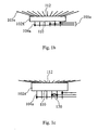
- Fig. 1a shows a display element 100 such as a display for a mobile phone, a PC or a TV.
- the pixels of the pixel matrix 101 are arranged in a matrix.
- the pixels are controlled via the control lines 103x and 103y.
- the driver circuits 102x and 102y are additionally present on the substrate.
- the driver circuits are applied to the substrate during fabrication.
- the driver circuits are supplied with signals from an external drive via the pads 104b.
- the signals are transmitted via the leads 104a to the driver circuits.
- the pads 104b and the leads 104a together form the contactable surfaces. These are also referred to below as contact surfaces.
- these pads can not be made large enough on the limited space available to ensure efficient and safe testing.
- these prior art contact pads have a size of 4 inches (640 x 480 pixels) for a display Size from approx. 60 ⁇ m to 2000 ⁇ m.
- a test pattern must be generated via an external control.
- the contacting of the pads 104b must be safe and reliable. Due to the size of the display element, it may be necessary to move the display under the electron beam.
- the contact with the movement during testing must be carried continuously, or it must be solved and restored as quickly and safely as possible.
- the devisierblock which accomplishes the contacting, must be functional under vacuum conditions and must not disturb an electron beam or the electron to be detected by electromagnetic fields.
- the pixel matrix 101 must not be covered by the contacting mechanism, since otherwise a test with an electron beam is no longer possible.
- additional contact surfaces are provided for testing. These consist of the pads 105b and the associated leads 105a. Since no arbitrary images - but only sufficiently complex patterns - have to be generated on the display for a test procedure, the number of these test contact areas can be reduced compared to the number of contact areas used for regular operation. In this case, the number of test contact surfaces (105a and 105b) can be reduced to a maximum of 90%, preferably to a maximum of 50%, particularly preferably to a maximum of 20%, compared with the number of operating contact surfaces. In this way, for example, for a large display in addition to the approximately 200 contact surfaces for normal operation about another 30 contact surfaces for the test method provided. Whereas for a smaller display with about 30 contact surfaces for normal operation about another 5 test contact surfaces are provided.
- the number of inputs of the driver circuit 102x amounts to a maximum of 5% of the number of outputs of the driver circuit, by means of which the driver circuit with the control lines 103x is connected to the matrix of pixels 101. That means:
- the pads used during testing are connected via control lines to the outputs of a possible driver circuit. These are usually the shorting bars that are attached to the control lines.
- the pads for generating a text image are connected to the driver circuit via the inputs of the driver circuit. The number of connections of the test pads to the inputs of the driver circuit is reduced compared to the number of outputs of the driver circuit connected to the control lines.
- the contact surfaces used for the testing process such that the pads 105b have at least an extension of 100 ⁇ m, preferably of at least 0.5 mm, particularly preferably of at least 2 mm.
- Extension means the dimension in the direction in which the smallest value for the dimension results. Consequently, in the case of a rectangular pad, the length of the shorter side would be considered as extension.
- the above-mentioned extent of the contact surfaces allows a safe, fast and trouble-free contact.
- test pads 105b are connected to the leads 104a via the leads 105a according to a first embodiment.
- the leads 104a are used for the pads 104b of regular operation.
- one or more test pads may be connected to the inputs of driver circuits 102x and / or 102y.
- a test pad it is possible for a test pad to be connected to multiple leads 104a for normal image formation via switching elements or devices (eg, diodes, transistors, or otherwise).
- An example of such a connection is shown in FIG. 1c with the switching or component 120.
- Another way to connect multiple leads to a test pad is a connection structure that is removed for normal operation. That is, the structure is separated, for example, in glass separation or by etching processes.
- the present invention accordingly also relates to optoelectronic devices, for example in the form of displays, which are equipped for a test method with first and second arrangements of contact surfaces according to the invention, with which the test method according to the invention is carried out and in which at least parts of the test arrangement of contact surfaces is separated after the test procedure.
- test pads 105b may also be connected to operating pads 104b by means of the leads 105a of the test pads, without thereby departing from the inventive idea.
- the terminals of a driver circuit 102x are shown in FIG. 1b.
- the control lines 103x for the pixel array 101 (not shown in FIG. 1b) are connected to the outputs of the driver circuit 102x.
- the leads 104a and 105a are connected to the inputs of the driver circuit.
- the term "output" of the driver circuit is to be understood such that the outputs are connected to the control lines which are used for the taxation of the individual pixels.
- An input of the driver circuit is understood to mean a terminal via which the driver circuits are supplied with external signals. In the process, these external signals are modified in the driver circuit, in order then to supply the control lines 103x connected to the outputs with signals for the picture elements.
- FIG. 2 shows a schematic illustration of a further embodiment of a display element 100.
- the test contact surfaces (105a + 105b) are shown here Embodiment via test driver circuits 202x and 202y connected to the driver circuits 102x and 102y, respectively.
- test drive circuits 202x and 202y serve to convert the signals obtained from the test pads (105a and 105b) into signals for the drive circuits 102x and 102y.
- the driver circuits 102 may then further process these converted signals for pattern generation and supply them to the pixels by means of the control lines 103.
- test driver circuits 202 For the test driver circuits 202, several implementations are possible. On the one hand, an embodiment similar to FIG. 3 can be realized.
- the test driver circuit thereby provides inputs for the test pads and forwards the signals to corresponding contacts of the driver circuits 102 on.
- a memory is integrated in the test driver circuit 202.
- One or more test patterns are stored in the memory. Via external signals, which are provided via the test pads 105, the generation of a test pattern is started or stopped. In the case of several stored test patterns, one of the patterns is additionally selected by the external signal.
- the test driver circuit transmits the signals necessary for the test pattern to the driver circuits 102. Based on these signals, the test pattern is generated. According to this embodiment, it is possible to further reduce the number of pads required for a test procedure. If the generation of the test pattern merely needs to be started or stopped, the number of test pads may preferably be reduced to the pads for the power supplies and a control pad.
- the test driver circuit 202 may perform the function of a multiplexer. For example, by temporally multiplexing the signals, it becomes possible to provide a plurality of signals over a small number of test pads 105b.
- the buffer necessary for this or any timer modules are also integrated in this embodiment on the chip of one of the driver circuits.
- the test pads 105 are connected directly to inputs of the driver circuit (s).
- a test driver circuit 202 can be integrated in the driver circuit 102 in such a way that it is spoken by a single driver circuit 102 must become.
- the driver circuit provides inputs for generating a test pattern and these inputs are connected to test pads.
- inputs 110 and outputs 112 of the driver circuit 102 can also be distinguished in FIG. 3b.
- test pattern As can be produced by the present invention, is shown in FIG.
- Fig. 4 the individual pixels, d. H. the pixels, shown as boxes.
- the letters in the boxes symbolize a potential to which the electrodes of the pixels are charged when generating a test pattern.
- Which of the pixels A to D is assigned to which potential is determined within the setup for the test.
- test pattern due to the periodic arrangement of the potentials of the electrodes of the pixels all degrees of freedom that are sufficient for a test pattern, can be exhausted.
- a pattern corresponding to the letters A to H can be generated.
- a different potential value can be assigned to each adjacent pixel on the basis of one pixel.
- the drive for such a periodic pattern is less complex than the generation of any image. Therefore, it is possible to reduce the number of test pads compared to the number of operating pads. This allows an increase in the contact surfaces used in a test procedure. According to the present invention, this leads to an improved test method, since errors in the contacting can be reduced.
- the mechanism for contacting the display to be tested can be designed for speed. This optimization can additionally speed up the test procedure. As a result, the throughput of the piece goods to be tested is increased.
- a beam of charged particles such as an electron or ion beam, or a laser beam
- the corpuscular beam is understood as meaning both a laser beam, in which the particles are photons, and a particle beam, in which the particles are ions, atoms, electrons, or other particles.
- test method based on an electron beam, without the invention being restricted thereto.
- the test method consists in charging the electrodes of the picture elements to a potential via the supply lines. This potential or its temporal change can be measured with the corpuscular beam. Defects such as short circuits or missing contacts can be detected as well as parasitic elements and their size.
- the electrodes of the pixels are charged via a corpuscular beam and the resulting potentials are also measured with a particle beam.
- the control of the supply lines determines the initial and boundary conditions.
- the electrodes of the picture elements are charged via a particle beam and the current thereby caused in the leads is measured.
- the driver circuit it may be necessary to design the driver circuit so that such a measurement of the current to externally accessible contacts on the driver circuit is possible.
- the pads of the display elements must be connected to an external controller or external gauges. This contacting can be improved by the device of the present invention.
- the display under test is first placed in a chamber and placed under the electron beam.
- the chamber must be evacuated to a pressure below 10 -4 mbar.
- a contacting block is connected to the test contact surfaces according to the invention.
- the contacting block is a mechanism with which a test system makes electrical contact with the contact surfaces of the display in general. There is a transmission of signals to the contact surfaces. Depending on the signals, the electrodes or individual electrodes of the picture elements are charged to defined potentials. This generates a test pattern.
- the control of the test system tests the potentials of individual electrodes.
- an area of the display is first tested and the display then moved by means of a displacement unit.
- a displacement unit For a reliable test, it is important that the contact with the pads is maintained continuously or can be restored reliably and quickly. This is possible according to the present invention through the test pads. After the shift, another area is tested. The interplay of displacement of the display element and testing of an area can continue until the entire display has been tested or all displays on the substrate have been tested.
- the test speed is important for the test method described above.
- the measurement must be very reliable, since already about 0.1 per thousand defective pixels prevent use of the display.
- error correction can take place, for example, by an ion beam or laser beam.
- the devices of the present invention are advantageous for the test method according to the invention described, since the test contact surfaces simplify the contacting of the display within the test system. As a result, it is possible to realize a contact efficiently.
- the contacting satisfies the above boundary conditions.
- the second array of pads is connected to the driver circuit via the first array of pads.
- the contact surfaces for generating the test pattern can be connected to a plurality of contact surfaces for regular operation.
- the number of test pads compared to the number of regular pads can be reduced particularly preferably by not connecting all pads connected to the driver circuit to a test pad.
- the second arrangement of contact surfaces is connected via a test electronics to the driver circuit. It is particularly preferred if the test electronics contains a memory from which the test pattern to be generated is read. This test pattern can be provided to the driver circuit.
- the second array of pads is directly connected to the driver circuit. It is particularly advantageous if the driver circuit is such that it contains circuits for processing the signals from the test pads for the test patterns.
- the above-mentioned aspects serve to further simplify the testing process, by separating between contact areas for the testing process and for the regular image generation. Moreover, due to these preferred aspects, it is possible to reduce the number of contact areas for the test and thus offer the option of increased contact areas for the test procedure.
- the number of second pads of the second array of pads is at most 90% of the number of first pads of the first array of pads.
- the number of second pads is preferably at most 50%, particularly preferably at most 20%, of the number of first contact surfaces. This makes it possible and is particularly advantageous to provide the second pads of the second arrangement of contact surfaces with at least an extension of 100 ⁇ m, preferably an extension of 0.5 mm, particularly preferably an extension of 2 mm.
- test driver circuit includes a memory
- the number of second pads of the second array of pads used for signal transmission is one.
- the input signals When testing an opto-electronic device according to the present invention, it is preferable if the input signals generate a periodic test pattern. Periodic test patterns are particularly preferred in the vertical, horizontal and diagonal directions.
- the present invention provides particular advantages when using a vacuum in the environment of the optoelectronic device under test or when the test method involves the steps of: testing the picture elements in a region of the matrix of pixels or all pixels of a smaller matrix; Moving the optoelectronic device and testing of pixels in another area of the matrix of pixels or another small matrix.
Landscapes
- Physics & Mathematics (AREA)
- Nonlinear Science (AREA)
- General Physics & Mathematics (AREA)
- Engineering & Computer Science (AREA)
- Chemical & Material Sciences (AREA)
- Crystallography & Structural Chemistry (AREA)
- Optics & Photonics (AREA)
- Computer Hardware Design (AREA)
- Theoretical Computer Science (AREA)
- Mathematical Physics (AREA)
- Control Of Indicators Other Than Cathode Ray Tubes (AREA)
- Liquid Crystal (AREA)
- Liquid Crystal Display Device Control (AREA)
- Devices For Indicating Variable Information By Combining Individual Elements (AREA)
- Tests Of Electronic Circuits (AREA)
- Light Receiving Elements (AREA)
- Led Devices (AREA)
- Structures Or Materials For Encapsulating Or Coating Semiconductor Devices Or Solid State Devices (AREA)
- Testing Of Individual Semiconductor Devices (AREA)
- Testing Of Optical Devices Or Fibers (AREA)
- Solid State Image Pick-Up Elements (AREA)
Claims (21)
- Dispositif de commande électronique pour la commande d'un appareil optoélectronique avec une matrice d'éléments d'image, avec :un circuit d'attaque (102x),le dispositif d'attaque présentant des entrées (110) et des sorties (112);un premier ensemble de surfaces de contact (104), lesquelles sont en liaison avec les entrées du dispositif d'attaque (102x); etun deuxième ensemble de surfaces de contact (105), lesquelles sont en liaison avec les entrées du circuit d'attaque (102x),les surfaces de contact (105) du deuxième ensemble de surfaces de contact étant plus grandes que les surfaces de contact (104) du premier ensemble de surfaces de contact.
- Dispositif de commande électronique selon la revendication précédente, dans lequel :le nombre d'entrées du circuit d'attaque (102x) grâce auxquelles le circuit d'attaque est en liaison avec le deuxième ensemble de surfaces de contact (105) représentant au maximum 5% du nombre de sorties du circuit d'attaque, grâce auxquelles le circuit d'attaque est en liaison avec les lignes pilote (103x) de la matrice d'éléments d'image (101).
- Dispositif de commande électronique selon l'une quelconque des revendications précédentes, dans lequel :le premier ensemble de surfaces de contact (104) sert à la formation d'images pendant le fonctionnement normal ; etle deuxième ensemble de surfaces de contact (105) servant à la formation de motifs pendant le fonctionnement de test.
- Dispositif de commande électronique selon l'une quelconque des revendications précédentes, dans lequel
le deuxième ensemble de surfaces de contact (105) est en liaison, via le premier ensemble de surfaces de contact (104), avec le circuit d'attaque (102x). - Dispositif de commande électronique selon la revendication 4, dans lequel :le deuxième ensemble de surfaces de contact (105) est en liaison avec le circuit d'attaque (102x) via le premier ensemble de surfaces de contact (104), à l'aide d'éléments de commutation ou de composants.
- Dispositif de commande électronique selon la revendication 4, dans lequel
le deuxième ensemble de surfaces de contact (105) est directement en liaison, via le premier ensemble de surfaces de contact (104), avec le circuit d'attaque (102x). - Dispositif de commande électronique selon l'une des revendications 1 à 3, dans lequel
le deuxième ensemble de surfaces de contact (105) est en liaison, via un dispositif électronique de test (202x), avec le circuit d'attaque (102x). - Dispositif de commande électronique selon l'une des revendications 1 à 3, dans lequel :
le deuxième ensemble de surfaces de contact (105) est directement en liaison avec le circuit d'attaque. - Dispositif de commande électronique selon la revendication 8, dans lequel :des circuits de commutation de test sont intégrés dans le circuit d'attaque.
- Dispositif de commande électronique selon l'une quelconque des revendications précédentes, dans lequel :le nombre de deuxièmes pastilles (105b) du deuxième ensemble de surfaces de contact (105) représente au maximum 90% du nombre de premières pastilles (104b) du premier ensemble de surfaces de contact (104), et représente de préférence un maximum de 50%, et de manière particulièrement préférée, un maximum de 20%.
- Dispositif de commande électronique selon l'une des revendications précédentes, dans lequel :les deuxièmes pastilles (105b) du deuxième ensemble de surfaces de contact sont plus grandes que les premières pastilles (104b) du premier ensemble de surfaces de contact.
- Dispositif de commande électronique selon l'une quelconque des revendications précédentes, dans lequel :les deuxièmes pastilles (105b) du deuxième ensemble de surfaces de contact présentent un étalement de 100µm, de préférence un étalement de 0,5 mm, et de manière particulièrement préférée un étalement de 2 mm.
- Appareil optoélectronique avec
une matrice d'éléments d'image (101) ; et
un dispositif électronique de commande selon l'une quelconque des revendications 1 à 12. - Appareil optoélectronique selon la revendication 13, dans lequel au moins des parties du deuxième ensemble de surfaces de contact sont séparées.
- Procédé pour tester un appareil optoélectronique comprenant les étapes suivantes :a) établissement d'un contact entre une commande externe et un ensemble de surfaces de contact de test, lesquelles sont plus grandes que des surfaces de contact de fonctionnement ;b) alimentation d'une entrée d'un circuit d'attaque avec des signaux d'entrée via l'ensemble de surfaces de contact de test, afin de produire un motif de test sur une matrice d'éléments d'image ; etc) test des éléments d'image d'éléments d'image.
- Procédé de test selon la revendication 15 dans lequel
les signaux d'entrée génèrent un motif de test périodique. - Procédé de test selon l'une quelconque des revendications 15 à 16 dans lequel
les signaux d'entrée génèrent un motif de test périodique vertical, horizontal, ou diagonal. - Procédé de test selon l'une quelconque des revendications 15 à 17 dans lequel
les éléments d'image sont testés avec un faisceau de particules chargées ou un faisceau laser. - Procédé de test selon l'une quelconque des revendications 15 à 18, comprenant l'étape suivante :établissement d'un vide dans l'environnement de l'appareil optoélectronique à tester.
- Procédé de test selon l'une quelconque des revendications 15 à 19, dans lequel l'étape c) comprend les étapes suivantes :c1) les éléments d'images dans une zone de la matrice d'éléments d'image sont testés ;c2) l'appareil optoélectronique est déplacé ; etc3) les éléments d'image dans une autre zone de la matrice d'éléments d'image sont testés.
- Procédé de fabrication d'un dispositif de commande électronique d'un appareil optoélectronique avec une matrice d'éléments d'image comprenant les étapes suivantes :a) un circuit d'attaque est mis à disposition;b) des lignes pilote de la matrice d'éléments d'image sont reliées au circuit d'attaque ;c) un premier ensemble de surfaces de contact est mis à disposition ;d) le premier ensemble de surfaces de contact est relié aux entrées du circuit d'attaque ;e) un deuxième ensemble de surfaces de contact est mis à disposition, dont les surfaces de contact sont plus grandes que les surfaces de contact du premier ensemble de surfaces de contact ; etf) le deuxième ensemble de surfaces de contact est relié à des entrées du circuit d'attaque.
Applications Claiming Priority (3)
| Application Number | Priority Date | Filing Date | Title |
|---|---|---|---|
| DE10227332 | 2002-06-19 | ||
| DE10227332A DE10227332A1 (de) | 2002-06-19 | 2002-06-19 | Ansteuervorrichtung mit verbesserten Testeneigenschaften |
| PCT/EP2003/006481 WO2004001706A2 (fr) | 2002-06-19 | 2003-06-18 | Dispositif de commande presentant de meilleures proprietes d'essai |
Publications (2)
| Publication Number | Publication Date |
|---|---|
| EP1521973A2 EP1521973A2 (fr) | 2005-04-13 |
| EP1521973B1 true EP1521973B1 (fr) | 2007-07-25 |
Family
ID=29723271
Family Applications (1)
| Application Number | Title | Priority Date | Filing Date |
|---|---|---|---|
| EP03760655A Expired - Lifetime EP1521973B1 (fr) | 2002-06-19 | 2003-06-18 | Dispositif de commande presentant de meilleures proprietes d'essai |
Country Status (8)
| Country | Link |
|---|---|
| US (2) | US20050212782A1 (fr) |
| EP (1) | EP1521973B1 (fr) |
| JP (1) | JP4444102B2 (fr) |
| KR (1) | KR100980120B1 (fr) |
| AT (1) | ATE368232T1 (fr) |
| DE (2) | DE10227332A1 (fr) |
| TW (1) | TWI345751B (fr) |
| WO (1) | WO2004001706A2 (fr) |
Families Citing this family (11)
| Publication number | Priority date | Publication date | Assignee | Title |
|---|---|---|---|---|
| DE10227332A1 (de) * | 2002-06-19 | 2004-01-15 | Akt Electron Beam Technology Gmbh | Ansteuervorrichtung mit verbesserten Testeneigenschaften |
| TWI333094B (en) * | 2005-02-25 | 2010-11-11 | Au Optronics Corp | System and method for display testing |
| JP4665677B2 (ja) * | 2005-09-09 | 2011-04-06 | セイコーエプソン株式会社 | 集積回路装置及び電子機器 |
| KR20080008704A (ko) * | 2006-07-21 | 2008-01-24 | 삼성전자주식회사 | 표시기판, 그 제조방법 및 이를 갖는 표시장치 |
| US8115506B2 (en) * | 2007-05-14 | 2012-02-14 | Applied Materials, Inc. | Localization of driver failures within liquid crystal displays |
| JP4692566B2 (ja) * | 2008-03-28 | 2011-06-01 | ブラザー工業株式会社 | 通信装置 |
| WO2012086623A1 (fr) | 2010-12-24 | 2012-06-28 | 日本ゼオン株式会社 | Élément électroluminescent |
| CN105954899B (zh) * | 2016-07-08 | 2019-07-23 | 武汉华星光电技术有限公司 | 液晶显示面板以及液晶显示器 |
| KR102456696B1 (ko) * | 2018-08-07 | 2022-10-19 | 삼성디스플레이 주식회사 | 표시 패널 및 그 제조 방법 |
| CN110444117B (zh) * | 2019-07-24 | 2021-09-28 | 苏州清越光电科技股份有限公司 | 封装基板及显示面板的制备方法 |
| CN111261055B (zh) * | 2020-01-21 | 2022-02-22 | 京东方科技集团股份有限公司 | Oled显示屏及oled显示装置 |
Family Cites Families (125)
| Publication number | Priority date | Publication date | Assignee | Title |
|---|---|---|---|---|
| US3983401A (en) | 1975-03-13 | 1976-09-28 | Electron Beam Microfabrication Corporation | Method and apparatus for target support in electron projection systems |
| US4090056A (en) | 1976-05-17 | 1978-05-16 | Electron Beam Welding, Inc. | Optical viewing system for an electron beam welder |
| DE2902852C2 (de) | 1979-01-25 | 1983-04-07 | Siemens AG, 1000 Berlin und 8000 München | Flache Elektronenstrahl-Bildwiedergaberöhre |
| DE2937004C2 (de) | 1979-09-13 | 1984-11-08 | Fraunhofer-Gesellschaft zur Förderung der angewandten Forschung e.V., 8000 München | Chromatisch korrigierte Ablenkvorrichtung für Korpuskularstrahlgeräte |
| US4495966A (en) | 1982-05-24 | 1985-01-29 | Electron Beam Corporation | Separable high vacuum valve |
| JPS58210631A (ja) | 1982-05-31 | 1983-12-07 | Toshiba Corp | 電子ビ−ムを用いたicテスタ |
| US4456910A (en) * | 1982-08-12 | 1984-06-26 | General Electric Company | Non-complementary metal oxide semiconductor (MOS) driver for liquid crystal displays |
| US4528452A (en) | 1982-12-09 | 1985-07-09 | Electron Beam Corporation | Alignment and detection system for electron image projectors |
| EP0175933A1 (fr) | 1984-09-21 | 1986-04-02 | Siemens Aktiengesellschaft | Système de lentilles à balayage sans défauts chromatiques de déviation pour traitement de matériaux par faisceaux corpusculaires |
| US4985681A (en) | 1985-01-18 | 1991-01-15 | Siemens Aktiengesellschaft | Particle beam measuring method for non-contact testing of interconnect networks |
| JPS622552A (ja) | 1985-06-27 | 1987-01-08 | Matsushita Electric Ind Co Ltd | 半導体検査装置および半導体検査方法 |
| JPS6298544A (ja) | 1985-10-25 | 1987-05-08 | Hitachi Ltd | 荷電粒子線装置 |
| US4764818A (en) | 1986-02-03 | 1988-08-16 | Electron Beam Memories | Electron beam memory system with improved high rate digital beam pulsing system |
| US4740705A (en) | 1986-08-11 | 1988-04-26 | Electron Beam Memories | Axially compact field emission cathode assembly |
| US4760567A (en) | 1986-08-11 | 1988-07-26 | Electron Beam Memories | Electron beam memory system with ultra-compact, high current density electron gun |
| US4725736A (en) | 1986-08-11 | 1988-02-16 | Electron Beam Memories | Electrostatic electron gun with integrated electron beam deflection and/or stigmating system |
| US4965515A (en) | 1986-10-15 | 1990-10-23 | Tokyo Electron Limited | Apparatus and method of testing a semiconductor wafer |
| US4819038A (en) | 1986-12-22 | 1989-04-04 | Ibm Corporation | TFT array for liquid crystal displays allowing in-process testing |
| US4795912A (en) | 1987-02-17 | 1989-01-03 | Trw Inc. | Method and apparatus for correcting chromatic aberration in charged particle beams |
| NL8700933A (nl) | 1987-04-21 | 1988-11-16 | Philips Nv | Testmethode voor lcd-elementen. |
| KR960006869B1 (ko) | 1987-09-02 | 1996-05-23 | 도오교오 에레구토론 가부시끼가이샤 | 프로우브 장치에 의한 전기특성 검사방법 |
| US6288561B1 (en) | 1988-05-16 | 2001-09-11 | Elm Technology Corporation | Method and apparatus for probing, testing, burn-in, repairing and programming of integrated circuits in a closed environment using a single apparatus |
| JP2653099B2 (ja) * | 1988-05-17 | 1997-09-10 | セイコーエプソン株式会社 | アクティブマトリクスパネル,投写型表示装置及びビューファインダー |
| US4870357A (en) | 1988-06-03 | 1989-09-26 | Apple Computer, Inc. | LCD error detection system |
| US4862075A (en) | 1988-09-01 | 1989-08-29 | Photon Dynamics, Inc. | High frequency test head using electro-optics |
| US4983833A (en) | 1988-11-21 | 1991-01-08 | Siemens Aktiengesellschaft | Device for the detecting of charged secondary particles |
| US4985676A (en) | 1989-02-17 | 1991-01-15 | Tokyo Electron Limited | Method and apparatus of performing probing test for electrically and sequentially testing semiconductor device patterns |
| EP0402499A1 (fr) | 1989-06-13 | 1990-12-19 | Siemens Aktiengesellschaft | Procédé pour tester une carte de circuits avec un faisceau de particules |
| US5124635A (en) | 1990-02-15 | 1992-06-23 | Photon Dynamics, Inc. | Voltage imaging system using electro-optics |
| US5177437A (en) | 1990-08-08 | 1993-01-05 | Photon Dynamics, Inc. | High-density optically-addressable circuit board probe panel and method for use |
| US5285150A (en) | 1990-11-26 | 1994-02-08 | Photon Dynamics, Inc. | Method and apparatus for testing LCD panel array |
| US5081687A (en) * | 1990-11-30 | 1992-01-14 | Photon Dynamics, Inc. | Method and apparatus for testing LCD panel array prior to shorting bar removal |
| US6320568B1 (en) * | 1990-12-31 | 2001-11-20 | Kopin Corporation | Control system for display panels |
| US5170127A (en) | 1991-02-19 | 1992-12-08 | Photon Dynamics, Inc. | Capacitance imaging system using electro-optics |
| JPH05136218A (ja) | 1991-02-19 | 1993-06-01 | Tokyo Electron Yamanashi Kk | 検査装置 |
| JPH04326725A (ja) | 1991-04-26 | 1992-11-16 | Tokyo Electron Ltd | プラズマ装置 |
| US5175495A (en) | 1991-04-30 | 1992-12-29 | Lsi Logic Corporation | Detection of semiconductor failures by photoemission and electron beam testing |
| DE69223088T2 (de) | 1991-06-10 | 1998-03-05 | Fujitsu Ltd | Apparat zur Musterüberprüfung und Elektronenstrahlgerät |
| US5432461A (en) * | 1991-06-28 | 1995-07-11 | Photon Dynamics, Inc. | Method of testing active matrix liquid crystal display substrates |
| US5268638A (en) | 1991-07-15 | 1993-12-07 | Siemens Aktiengesellschaft | Method for particle beam testing of substrates for liquid crystal displays "LCD" |
| DE4123959C1 (fr) | 1991-07-19 | 1993-02-04 | Man Roland Druckmaschinen Ag, 6050 Offenbach, De | |
| US5504438A (en) | 1991-09-10 | 1996-04-02 | Photon Dynamics, Inc. | Testing method for imaging defects in a liquid crystal display substrate |
| US5258706A (en) | 1991-10-16 | 1993-11-02 | Siemens Aktiengesellschaft | Method for the recognition of testing errors in the test of microwirings |
| US5369359A (en) | 1991-11-05 | 1994-11-29 | Siemens Aktiengesellschaft | Particle beam testing method with countervoltage or retarding voltage follow-up or feedback |
| US5313156A (en) | 1991-12-04 | 1994-05-17 | Advantest Corporation | Apparatus for automatic handling |
| US5546013A (en) * | 1993-03-05 | 1996-08-13 | International Business Machines Corporation | Array tester for determining contact quality and line integrity in a TFT/LCD |
| JP3334719B2 (ja) | 1993-09-16 | 2002-10-15 | 倭 窪田 | 創傷被覆用材料および創傷被覆用組成物 |
| DE69326003T2 (de) | 1993-09-20 | 1999-11-25 | Hewlett-Packard Gmbh | Testapparat zum Testen und Handhaben einer Vielzahl von Vorrichtungen |
| US5644245A (en) | 1993-11-24 | 1997-07-01 | Tokyo Electron Limited | Probe apparatus for inspecting electrical characteristics of a microelectronic element |
| US5528158A (en) | 1994-04-11 | 1996-06-18 | Xandex, Inc. | Probe card changer system and method |
| EP0686958B1 (fr) | 1994-06-06 | 2003-10-29 | Canon Kabushiki Kaisha | Compensation de courant continu pour un affichage entrelacé |
| JP3247799B2 (ja) * | 1994-06-09 | 2002-01-21 | シャープ株式会社 | 液晶表示パネルおよびその検査方法 |
| KR100283851B1 (ko) | 1994-07-11 | 2001-04-02 | 기리야마 겐지 | 모니터 장치 및 모니터 방법 |
| US5691764A (en) | 1994-08-05 | 1997-11-25 | Tokyo Electron Limited | Apparatus for examining target objects such as LCD panels |
| US5657139A (en) * | 1994-09-30 | 1997-08-12 | Kabushiki Kaisha Toshiba | Array substrate for a flat-display device including surge protection circuits and short circuit line or lines |
| JPH08201841A (ja) * | 1994-11-24 | 1996-08-09 | Toshiba Electron Eng Corp | 表示装置及びその検査方法 |
| US5558717A (en) | 1994-11-30 | 1996-09-24 | Applied Materials | CVD Processing chamber |
| US5742173A (en) | 1995-03-18 | 1998-04-21 | Tokyo Electron Limited | Method and apparatus for probe testing substrate |
| US5621333A (en) | 1995-05-19 | 1997-04-15 | Microconnect, Inc. | Contact device for making connection to an electronic circuit device |
| DE19525081B4 (de) | 1995-07-10 | 2006-06-29 | Display Products Group, Inc., Hayward | Verfahren und Vorrichtung zum Testen der Funktion von Mikrostrukturelementen |
| KR100291316B1 (ko) | 1995-07-14 | 2001-06-01 | 히가시 데쓰로 | Lcd 검사장치 |
| JPH0980460A (ja) * | 1995-09-07 | 1997-03-28 | Seiko Instr Inc | 液晶表示装置及びその検査方法 |
| TW331599B (en) * | 1995-09-26 | 1998-05-11 | Toshiba Co Ltd | Array substrate for LCD and method of making same |
| CN101369579B (zh) * | 1995-10-03 | 2011-05-04 | 精工爱普生株式会社 | 有源矩阵基板的制造方法和薄膜元件的制造方法 |
| US5892224A (en) | 1996-05-13 | 1999-04-06 | Nikon Corporation | Apparatus and methods for inspecting wafers and masks using multiple charged-particle beams |
| US6046599A (en) | 1996-05-20 | 2000-04-04 | Microconnect, Inc. | Method and device for making connection |
| TW329002B (en) * | 1996-06-05 | 1998-04-01 | Zenshin Test Co | Apparatus and method for inspecting a LCD substrate |
| US6243208B1 (en) * | 1996-08-22 | 2001-06-05 | Canon Kabushiki Kaisha | Optical element, optical system using optical element, and optical device with optical element |
| CN1129025C (zh) * | 1997-01-13 | 2003-11-26 | 现代电子美国公司 | 改进型有源矩阵静电释放防护和测试方案 |
| US5923180A (en) | 1997-02-04 | 1999-07-13 | Hewlett-Packard Company | Compliant wafer prober docking adapter |
| JP3423979B2 (ja) | 1997-07-11 | 2003-07-07 | 東京エレクトロン株式会社 | プローブ方法及びプローブ装置 |
| JP4036923B2 (ja) | 1997-07-17 | 2008-01-23 | 株式会社半導体エネルギー研究所 | 表示装置およびその駆動回路 |
| US6337722B1 (en) * | 1997-08-07 | 2002-01-08 | Lg.Philips Lcd Co., Ltd | Liquid crystal display panel having electrostatic discharge prevention circuitry |
| JP4260250B2 (ja) * | 1997-09-25 | 2009-04-30 | 三星電子株式会社 | 静電気保護回路を有する液晶表示装置及びこの回路を利用した表示検査方法 |
| US6265889B1 (en) * | 1997-09-30 | 2001-07-24 | Kabushiki Kaisha Toshiba | Semiconductor test circuit and a method for testing a semiconductor liquid crystal display circuit |
| US6188453B1 (en) * | 1997-09-30 | 2001-02-13 | Sanyo Electric Co., Ltd. | Display apparatus having test elements under or bounded by the sealant |
| US5973323A (en) | 1997-11-05 | 1999-10-26 | Kla-Tencor Corporation | Apparatus and method for secondary electron emission microscope |
| US6075245A (en) | 1998-01-12 | 2000-06-13 | Toro-Lira; Guillermo L. | High speed electron beam based system for testing large area flat panel displays |
| DE19802848B4 (de) | 1998-01-26 | 2012-02-02 | Display Products Group,Inc. | Verfahren und Vorrichtung zum Testen eines Substrats |
| US5982190A (en) | 1998-02-04 | 1999-11-09 | Toro-Lira; Guillermo L. | Method to determine pixel condition on flat panel displays using an electron beam |
| US6086362A (en) | 1998-05-20 | 2000-07-11 | Applied Komatsu Technology, Inc. | Multi-function chamber for a substrate processing system |
| US6198299B1 (en) | 1998-08-27 | 2001-03-06 | The Micromanipulator Company, Inc. | High Resolution analytical probe station |
| US6343369B1 (en) | 1998-09-15 | 2002-01-29 | Microconnect, Inc. | Methods for making contact device for making connection to an electronic circuit device and methods of using the same |
| EP0999573B1 (fr) | 1998-11-06 | 2006-06-28 | ICT Integrated Circuit Testing Gesellschaft für Halbleiterprüftechnik mbH | Colonne de faisceau de particules chargées |
| JP3718355B2 (ja) * | 1998-11-26 | 2005-11-24 | 株式会社 日立ディスプレイズ | 液晶表示装置 |
| US6137303A (en) | 1998-12-14 | 2000-10-24 | Sony Corporation | Integrated testing method and apparatus for semiconductor test operations processing |
| JP2000180392A (ja) | 1998-12-15 | 2000-06-30 | Shimadzu Corp | 電子線マイクロアナライザー |
| US6344750B1 (en) | 1999-01-08 | 2002-02-05 | Schlumberger Technologies, Inc. | Voltage contrast method for semiconductor inspection using low voltage particle beam |
| JP2000223057A (ja) | 1999-01-28 | 2000-08-11 | Shimadzu Corp | 電子プローブマイクロアナライザー |
| US6437596B1 (en) * | 1999-01-28 | 2002-08-20 | International Business Machines Corporation | Integrated circuits for testing a display array |
| US6380729B1 (en) * | 1999-02-16 | 2002-04-30 | Alien Technology Corporation | Testing integrated circuit dice |
| JP2000268764A (ja) | 1999-03-18 | 2000-09-29 | Shimadzu Corp | 電子線自動分析装置 |
| US6452175B1 (en) | 1999-04-15 | 2002-09-17 | Applied Materials, Inc. | Column for charged particle beam device |
| US6614026B1 (en) | 1999-04-15 | 2003-09-02 | Applied Materials, Inc. | Charged particle beam column |
| JP2000311930A (ja) | 1999-04-28 | 2000-11-07 | Agilent Technologies Japan Ltd | 半導体検査装置と半導体検査装置におけるウエハ上の各ダイの属性を指定する方法 |
| US6281701B1 (en) * | 1999-06-04 | 2001-08-28 | Chi Mei Optoelectronics Corporation | Apparatus for testing flat panel display |
| WO2001001438A1 (fr) | 1999-06-23 | 2001-01-04 | Applied Materials, Inc. | Dispositif generateur de faisceaux ioniques |
| JP4045696B2 (ja) | 1999-07-22 | 2008-02-13 | 株式会社島津製作所 | X線分光器 |
| JP2001053282A (ja) | 1999-08-11 | 2001-02-23 | Matsushita Electric Ind Co Ltd | 薄膜トランジスタアレイ基板及びその検査方法 |
| TW533319B (en) * | 1999-11-19 | 2003-05-21 | De & T Co Ltd | LCD testing system |
| JP2001215463A (ja) * | 2000-02-02 | 2001-08-10 | Seiko Epson Corp | Lcdドライバのコモン出力設定回路及び設定方法並びにlcdドライバ用半導体装置 |
| JP2001318116A (ja) | 2000-05-11 | 2001-11-16 | Micronics Japan Co Ltd | 表示用パネル基板の検査装置 |
| JP2001330639A (ja) * | 2000-05-24 | 2001-11-30 | Toshiba Corp | アレイ基板の検査方法 |
| JP3937692B2 (ja) | 2000-06-15 | 2007-06-27 | セイコーエプソン株式会社 | アレイ基板の検査方法、アレイ基板の製造方法、アレイ基板及び電気光学装置 |
| US6828587B2 (en) | 2000-06-19 | 2004-12-07 | Semiconductor Energy Laboratory Co., Ltd. | Semiconductor device |
| JP4517323B2 (ja) | 2000-07-19 | 2010-08-04 | 株式会社島津製作所 | 電子線マイクロアナライザーの測定データ補正方法 |
| KR100385082B1 (ko) * | 2000-07-27 | 2003-05-22 | 삼성전자주식회사 | 액정 표시 장치 |
| JP2002040464A (ja) * | 2000-07-31 | 2002-02-06 | Sony Corp | 液晶表示パネル |
| JP2002048740A (ja) | 2000-07-31 | 2002-02-15 | Shimadzu Corp | 電子線分析装置 |
| JP2004523880A (ja) | 2000-09-15 | 2004-08-05 | アプライド マテリアルズ インコーポレイテッド | 処理装置用ダブル二重スロット式ロードロック |
| US20020135395A1 (en) | 2001-02-08 | 2002-09-26 | Pete Smith | System and method for testing a display device |
| JP2002257997A (ja) | 2001-03-01 | 2002-09-11 | Shimadzu Corp | 荷電粒子ビーム安定化装置 |
| JP2002343294A (ja) | 2001-03-12 | 2002-11-29 | Jeol Ltd | 複合電子顕微鏡 |
| JP2002310959A (ja) | 2001-04-16 | 2002-10-23 | Shimadzu Corp | 電子線分析装置 |
| US6777675B2 (en) | 2001-04-18 | 2004-08-17 | Multibeam | Detector optics for electron beam inspection system |
| US20030085855A1 (en) * | 2001-07-17 | 2003-05-08 | Kabushiki Kaisha Toshiba | Array substrate, method of inspecting array substrate, and liquid crystal display |
| JP2003050380A (ja) * | 2001-08-07 | 2003-02-21 | Toshiba Corp | アレイ基板の検査方法 |
| US7129694B2 (en) | 2002-05-23 | 2006-10-31 | Applied Materials, Inc. | Large substrate test system |
| JP4126484B2 (ja) | 2002-06-10 | 2008-07-30 | 株式会社島津製作所 | X線装置 |
| DE10227332A1 (de) * | 2002-06-19 | 2004-01-15 | Akt Electron Beam Technology Gmbh | Ansteuervorrichtung mit verbesserten Testeneigenschaften |
| US6765203B1 (en) | 2003-01-31 | 2004-07-20 | Shimadzu Corporation | Pallet assembly for substrate inspection device and substrate inspection device |
| US7355418B2 (en) | 2004-02-12 | 2008-04-08 | Applied Materials, Inc. | Configurable prober for TFT LCD array test |
| US6833717B1 (en) | 2004-02-12 | 2004-12-21 | Applied Materials, Inc. | Electron beam test system with integrated substrate transfer module |
| US7518602B2 (en) * | 2004-12-06 | 2009-04-14 | Semiconductor Energy Laboratory Co., Ltd. | Test circuit and display device having the same |
| US7532265B2 (en) * | 2005-06-08 | 2009-05-12 | Wintek Corporation | Integrated circuit with the cell test function for the electrostatic discharge protection |
-
2002
- 2002-06-19 DE DE10227332A patent/DE10227332A1/de not_active Withdrawn
-
2003
- 2003-06-16 TW TW092116249A patent/TWI345751B/zh not_active IP Right Cessation
- 2003-06-18 JP JP2004514792A patent/JP4444102B2/ja not_active Expired - Fee Related
- 2003-06-18 AT AT03760655T patent/ATE368232T1/de not_active IP Right Cessation
- 2003-06-18 US US10/518,780 patent/US20050212782A1/en not_active Abandoned
- 2003-06-18 WO PCT/EP2003/006481 patent/WO2004001706A2/fr not_active Ceased
- 2003-06-18 EP EP03760655A patent/EP1521973B1/fr not_active Expired - Lifetime
- 2003-06-18 DE DE50307773T patent/DE50307773D1/de not_active Expired - Lifetime
- 2003-06-18 KR KR1020047020388A patent/KR100980120B1/ko not_active Expired - Lifetime
-
2009
- 2009-01-16 US US12/355,698 patent/US8208114B2/en not_active Expired - Fee Related
Also Published As
| Publication number | Publication date |
|---|---|
| US8208114B2 (en) | 2012-06-26 |
| ATE368232T1 (de) | 2007-08-15 |
| TW200407824A (en) | 2004-05-16 |
| KR20050021007A (ko) | 2005-03-04 |
| DE50307773D1 (de) | 2007-09-06 |
| DE10227332A1 (de) | 2004-01-15 |
| US20090122056A1 (en) | 2009-05-14 |
| US20050212782A1 (en) | 2005-09-29 |
| WO2004001706A3 (fr) | 2004-02-26 |
| EP1521973A2 (fr) | 2005-04-13 |
| TWI345751B (en) | 2011-07-21 |
| JP4444102B2 (ja) | 2010-03-31 |
| KR100980120B1 (ko) | 2010-09-03 |
| WO2004001706A2 (fr) | 2003-12-31 |
| JP2005530211A (ja) | 2005-10-06 |
Similar Documents
| Publication | Publication Date | Title |
|---|---|---|
| DE10253717B4 (de) | Vorrichtung zum Kontaktieren für den Test mindestens eines Testobjekts, Testsystem und Verfahren zum Testen von Testobjekten | |
| DE69816593T2 (de) | Anzeigevorrichtung mit lichtleiterelement | |
| DE69216120T2 (de) | Verfahren zum Herstellen einer Elektrooptischen Vorrichtung | |
| DE69022248T2 (de) | Flüssigkristallanzeige mit redundanz der rasterabtastung. | |
| DE69531926T2 (de) | Mikrospiegel-Vorrichtung mit Herstellungsfehlern sowie Verfahren zu ihrem Betrieb | |
| DE68915413T2 (de) | Anzeigevorrichtung mit aktiver Matrix. | |
| DE69014397T2 (de) | Elektrophoretische Flachanzeigetafel mit einer doppelten Anode. | |
| EP2197014B1 (fr) | Dispositif d'exposition d'un substrat avec plusieurs faisceaux de particules chargées à forme variable pour la lithographie à haute résolution de motifs structurés | |
| DE112012006930B4 (de) | Array-Substrat und Flüssigkristallanzeigevorrichtung | |
| DE102005032520B4 (de) | Konfigurierbarer Prober zum Testen eines TFT LCD Arrays | |
| EP0523594B1 (fr) | Procédé pour tester des substrats pour dispositifs d'affichage à cristal liquide utilisant un faisceau corpusculaire | |
| DE69835131T2 (de) | D/A-Wandlerschaltung und Halbleiterbauelement | |
| DE112014003760B4 (de) | Elektronenmikroskop und Beobachtungsverfahren | |
| DE69330074T2 (de) | Flache Anzeigevorrichtung, ihr Ansteuerverfahren und Verfahren zu ihrer Herstellung | |
| DE69624322T2 (de) | Matrize auf Substrat und Herstellungsverfahren | |
| DE102013105470B4 (de) | Verfahren zum Herstellen einer Vorrichtung unter Verwendung eines elektrostatischen Chucks | |
| DE19800655A1 (de) | Dünnschichttransistoranordnung mit Schaltkreisen zur Vermeidung elektrostatischer Aufladungen | |
| DE102017205654A1 (de) | Array-Substrat, Anzeigetafel und Steuerungsverfahren | |
| DE19549022C2 (de) | Rasterelektronenmikroskop und Probenbetrachtungsverfahren mittels eines solchen | |
| DE112012006646T5 (de) | Detektionsschaltung und Verfahren zur Herstellung eines LCD-Paneels | |
| EP1521973A2 (fr) | Dispositif de commande presentant de meilleures proprietes d'essai | |
| DE19630334B4 (de) | Verfahren zum Herstellen einer Halbleitervorrichtung | |
| DE112014004151T5 (de) | Verfahren zur Korrektur der Neigung eines Strahls geladener Teilchen und mit einem Strahl geladener Teilchen arbeitende Vorrichtung | |
| DE4022711C2 (de) | Tunnelstromsonden-Verstellvorrichtung, Rastertunnel-Mikroskop und Datenspeichervorrichtung damit | |
| DE102019218315B3 (de) | Verfahren zur Spannungskontrastbildgebung mit einem Korpuskularvielstrahlmikroskop, Korpuskularvielstrahlmikroskop für Spannungskontrastbildgebung und Halbleiterstrukturen zur Spannungskontrastbildgebung mit einem Korpuskularvielstrahlmikroskop |
Legal Events
| Date | Code | Title | Description |
|---|---|---|---|
| PUAI | Public reference made under article 153(3) epc to a published international application that has entered the european phase |
Free format text: ORIGINAL CODE: 0009012 |
|
| 17P | Request for examination filed |
Effective date: 20050119 |
|
| AK | Designated contracting states |
Kind code of ref document: A2 Designated state(s): AT BE BG CH CY CZ DE DK EE ES FI FR GB GR HU IE IT LI LU MC NL PT RO SE SI SK TR |
|
| GRAP | Despatch of communication of intention to grant a patent |
Free format text: ORIGINAL CODE: EPIDOSNIGR1 |
|
| GRAS | Grant fee paid |
Free format text: ORIGINAL CODE: EPIDOSNIGR3 |
|
| GRAA | (expected) grant |
Free format text: ORIGINAL CODE: 0009210 |
|
| AK | Designated contracting states |
Kind code of ref document: B1 Designated state(s): AT BE BG CH CY CZ DE DK EE ES FI FR GB GR HU IE IT LI LU MC NL PT RO SE SI SK TR |
|
| REG | Reference to a national code |
Ref country code: GB Ref legal event code: FG4D Free format text: NOT ENGLISH |
|
| REG | Reference to a national code |
Ref country code: CH Ref legal event code: EP |
|
| REG | Reference to a national code |
Ref country code: IE Ref legal event code: FG4D Free format text: LANGUAGE OF EP DOCUMENT: GERMAN |
|
| REF | Corresponds to: |
Ref document number: 50307773 Country of ref document: DE Date of ref document: 20070906 Kind code of ref document: P |
|
| PG25 | Lapsed in a contracting state [announced via postgrant information from national office to epo] |
Ref country code: PT Free format text: LAPSE BECAUSE OF FAILURE TO SUBMIT A TRANSLATION OF THE DESCRIPTION OR TO PAY THE FEE WITHIN THE PRESCRIBED TIME-LIMIT Effective date: 20071226 Ref country code: BG Free format text: LAPSE BECAUSE OF FAILURE TO SUBMIT A TRANSLATION OF THE DESCRIPTION OR TO PAY THE FEE WITHIN THE PRESCRIBED TIME-LIMIT Effective date: 20071025 Ref country code: NL Free format text: LAPSE BECAUSE OF FAILURE TO SUBMIT A TRANSLATION OF THE DESCRIPTION OR TO PAY THE FEE WITHIN THE PRESCRIBED TIME-LIMIT Effective date: 20070725 Ref country code: FI Free format text: LAPSE BECAUSE OF FAILURE TO SUBMIT A TRANSLATION OF THE DESCRIPTION OR TO PAY THE FEE WITHIN THE PRESCRIBED TIME-LIMIT Effective date: 20070725 Ref country code: ES Free format text: LAPSE BECAUSE OF FAILURE TO SUBMIT A TRANSLATION OF THE DESCRIPTION OR TO PAY THE FEE WITHIN THE PRESCRIBED TIME-LIMIT Effective date: 20071105 |
|
| NLV1 | Nl: lapsed or annulled due to failure to fulfill the requirements of art. 29p and 29m of the patents act | ||
| GBV | Gb: ep patent (uk) treated as always having been void in accordance with gb section 77(7)/1977 [no translation filed] |
Effective date: 20070725 |
|
| REG | Reference to a national code |
Ref country code: IE Ref legal event code: FD4D |
|
| EN | Fr: translation not filed | ||
| PG25 | Lapsed in a contracting state [announced via postgrant information from national office to epo] |
Ref country code: DK Free format text: LAPSE BECAUSE OF FAILURE TO SUBMIT A TRANSLATION OF THE DESCRIPTION OR TO PAY THE FEE WITHIN THE PRESCRIBED TIME-LIMIT Effective date: 20070725 Ref country code: GR Free format text: LAPSE BECAUSE OF FAILURE TO SUBMIT A TRANSLATION OF THE DESCRIPTION OR TO PAY THE FEE WITHIN THE PRESCRIBED TIME-LIMIT Effective date: 20071026 |
|
| PG25 | Lapsed in a contracting state [announced via postgrant information from national office to epo] |
Ref country code: CZ Free format text: LAPSE BECAUSE OF FAILURE TO SUBMIT A TRANSLATION OF THE DESCRIPTION OR TO PAY THE FEE WITHIN THE PRESCRIBED TIME-LIMIT Effective date: 20070725 Ref country code: GB Free format text: LAPSE BECAUSE OF FAILURE TO SUBMIT A TRANSLATION OF THE DESCRIPTION OR TO PAY THE FEE WITHIN THE PRESCRIBED TIME-LIMIT Effective date: 20070725 Ref country code: IE Free format text: LAPSE BECAUSE OF FAILURE TO SUBMIT A TRANSLATION OF THE DESCRIPTION OR TO PAY THE FEE WITHIN THE PRESCRIBED TIME-LIMIT Effective date: 20070725 Ref country code: SK Free format text: LAPSE BECAUSE OF FAILURE TO SUBMIT A TRANSLATION OF THE DESCRIPTION OR TO PAY THE FEE WITHIN THE PRESCRIBED TIME-LIMIT Effective date: 20070725 |
|
| PLBE | No opposition filed within time limit |
Free format text: ORIGINAL CODE: 0009261 |
|
| STAA | Information on the status of an ep patent application or granted ep patent |
Free format text: STATUS: NO OPPOSITION FILED WITHIN TIME LIMIT |
|
| PG25 | Lapsed in a contracting state [announced via postgrant information from national office to epo] |
Ref country code: SE Free format text: LAPSE BECAUSE OF FAILURE TO SUBMIT A TRANSLATION OF THE DESCRIPTION OR TO PAY THE FEE WITHIN THE PRESCRIBED TIME-LIMIT Effective date: 20071025 Ref country code: RO Free format text: LAPSE BECAUSE OF FAILURE TO SUBMIT A TRANSLATION OF THE DESCRIPTION OR TO PAY THE FEE WITHIN THE PRESCRIBED TIME-LIMIT Effective date: 20070725 |
|
| 26N | No opposition filed |
Effective date: 20080428 |
|
| PG25 | Lapsed in a contracting state [announced via postgrant information from national office to epo] |
Ref country code: FR Free format text: LAPSE BECAUSE OF FAILURE TO SUBMIT A TRANSLATION OF THE DESCRIPTION OR TO PAY THE FEE WITHIN THE PRESCRIBED TIME-LIMIT Effective date: 20080321 |
|
| BERE | Be: lapsed |
Owner name: AKT ELECTRON BEAM TECHNOLOGY G.M.B.H. Effective date: 20080630 |
|
| PG25 | Lapsed in a contracting state [announced via postgrant information from national office to epo] |
Ref country code: MC Free format text: LAPSE BECAUSE OF NON-PAYMENT OF DUE FEES Effective date: 20080630 |
|
| REG | Reference to a national code |
Ref country code: CH Ref legal event code: PL |
|
| PG25 | Lapsed in a contracting state [announced via postgrant information from national office to epo] |
Ref country code: BE Free format text: LAPSE BECAUSE OF NON-PAYMENT OF DUE FEES Effective date: 20080630 |
|
| PG25 | Lapsed in a contracting state [announced via postgrant information from national office to epo] |
Ref country code: EE Free format text: LAPSE BECAUSE OF FAILURE TO SUBMIT A TRANSLATION OF THE DESCRIPTION OR TO PAY THE FEE WITHIN THE PRESCRIBED TIME-LIMIT Effective date: 20070725 |
|
| PG25 | Lapsed in a contracting state [announced via postgrant information from national office to epo] |
Ref country code: CH Free format text: LAPSE BECAUSE OF NON-PAYMENT OF DUE FEES Effective date: 20080630 Ref country code: SI Free format text: LAPSE BECAUSE OF FAILURE TO SUBMIT A TRANSLATION OF THE DESCRIPTION OR TO PAY THE FEE WITHIN THE PRESCRIBED TIME-LIMIT Effective date: 20070725 Ref country code: LI Free format text: LAPSE BECAUSE OF NON-PAYMENT OF DUE FEES Effective date: 20080630 |
|
| PG25 | Lapsed in a contracting state [announced via postgrant information from national office to epo] |
Ref country code: CY Free format text: LAPSE BECAUSE OF FAILURE TO SUBMIT A TRANSLATION OF THE DESCRIPTION OR TO PAY THE FEE WITHIN THE PRESCRIBED TIME-LIMIT Effective date: 20070725 |
|
| PG25 | Lapsed in a contracting state [announced via postgrant information from national office to epo] |
Ref country code: AT Free format text: LAPSE BECAUSE OF NON-PAYMENT OF DUE FEES Effective date: 20080618 |
|
| PG25 | Lapsed in a contracting state [announced via postgrant information from national office to epo] |
Ref country code: HU Free format text: LAPSE BECAUSE OF FAILURE TO SUBMIT A TRANSLATION OF THE DESCRIPTION OR TO PAY THE FEE WITHIN THE PRESCRIBED TIME-LIMIT Effective date: 20080126 Ref country code: LU Free format text: LAPSE BECAUSE OF NON-PAYMENT OF DUE FEES Effective date: 20080618 |
|
| PG25 | Lapsed in a contracting state [announced via postgrant information from national office to epo] |
Ref country code: TR Free format text: LAPSE BECAUSE OF FAILURE TO SUBMIT A TRANSLATION OF THE DESCRIPTION OR TO PAY THE FEE WITHIN THE PRESCRIBED TIME-LIMIT Effective date: 20070725 |
|
| PG25 | Lapsed in a contracting state [announced via postgrant information from national office to epo] |
Ref country code: IT Free format text: LAPSE BECAUSE OF NON-PAYMENT OF DUE FEES Effective date: 20080630 |
|
| PGFP | Annual fee paid to national office [announced via postgrant information from national office to epo] |
Ref country code: DE Payment date: 20120629 Year of fee payment: 10 |
|
| REG | Reference to a national code |
Ref country code: DE Ref legal event code: R119 Ref document number: 50307773 Country of ref document: DE Effective date: 20140101 |
|
| PG25 | Lapsed in a contracting state [announced via postgrant information from national office to epo] |
Ref country code: DE Free format text: LAPSE BECAUSE OF NON-PAYMENT OF DUE FEES Effective date: 20140101 |