EP1526569A2 - Metallkeramiksubstrat und seine Herstellungsmethode - Google Patents
Metallkeramiksubstrat und seine Herstellungsmethode Download PDFInfo
- Publication number
- EP1526569A2 EP1526569A2 EP04024974A EP04024974A EP1526569A2 EP 1526569 A2 EP1526569 A2 EP 1526569A2 EP 04024974 A EP04024974 A EP 04024974A EP 04024974 A EP04024974 A EP 04024974A EP 1526569 A2 EP1526569 A2 EP 1526569A2
- Authority
- EP
- European Patent Office
- Prior art keywords
- metal
- ceramic
- substrate
- ceramic substrate
- metal base
- Prior art date
- Legal status (The legal status is an assumption and is not a legal conclusion. Google has not performed a legal analysis and makes no representation as to the accuracy of the status listed.)
- Granted
Links
Images


Classifications
-
- H—ELECTRICITY
- H10—SEMICONDUCTOR DEVICES; ELECTRIC SOLID-STATE DEVICES NOT OTHERWISE PROVIDED FOR
- H10W—GENERIC PACKAGES, INTERCONNECTIONS, CONNECTORS OR OTHER CONSTRUCTIONAL DETAILS OF DEVICES COVERED BY CLASS H10
- H10W70/00—Package substrates; Interposers; Redistribution layers [RDL]
- H10W70/60—Insulating or insulated package substrates; Interposers; Redistribution layers
- H10W70/67—Insulating or insulated package substrates; Interposers; Redistribution layers characterised by their insulating layers or insulating parts
- H10W70/68—Shapes or dispositions thereof
- H10W70/6875—Shapes or dispositions thereof being on a metallic substrate, e.g. insulated metal substrates [IMS]
-
- H—ELECTRICITY
- H10—SEMICONDUCTOR DEVICES; ELECTRIC SOLID-STATE DEVICES NOT OTHERWISE PROVIDED FOR
- H10W—GENERIC PACKAGES, INTERCONNECTIONS, CONNECTORS OR OTHER CONSTRUCTIONAL DETAILS OF DEVICES COVERED BY CLASS H10
- H10W40/00—Arrangements for thermal protection or thermal control
- H10W40/20—Arrangements for cooling
- H10W40/25—Arrangements for cooling characterised by their materials
- H10W40/255—Arrangements for cooling characterised by their materials having a laminate or multilayered structure, e.g. direct bond copper [DBC] ceramic substrates
-
- H—ELECTRICITY
- H10—SEMICONDUCTOR DEVICES; ELECTRIC SOLID-STATE DEVICES NOT OTHERWISE PROVIDED FOR
- H10W—GENERIC PACKAGES, INTERCONNECTIONS, CONNECTORS OR OTHER CONSTRUCTIONAL DETAILS OF DEVICES COVERED BY CLASS H10
- H10W70/00—Package substrates; Interposers; Redistribution layers [RDL]
- H10W70/60—Insulating or insulated package substrates; Interposers; Redistribution layers
- H10W70/67—Insulating or insulated package substrates; Interposers; Redistribution layers characterised by their insulating layers or insulating parts
- H10W70/68—Shapes or dispositions thereof
-
- Y—GENERAL TAGGING OF NEW TECHNOLOGICAL DEVELOPMENTS; GENERAL TAGGING OF CROSS-SECTIONAL TECHNOLOGIES SPANNING OVER SEVERAL SECTIONS OF THE IPC; TECHNICAL SUBJECTS COVERED BY FORMER USPC CROSS-REFERENCE ART COLLECTIONS [XRACs] AND DIGESTS
- Y10—TECHNICAL SUBJECTS COVERED BY FORMER USPC
- Y10T—TECHNICAL SUBJECTS COVERED BY FORMER US CLASSIFICATION
- Y10T428/00—Stock material or miscellaneous articles
- Y10T428/12—All metal or with adjacent metals
- Y10T428/12493—Composite; i.e., plural, adjacent, spatially distinct metal components [e.g., layers, joint, etc.]
- Y10T428/12535—Composite; i.e., plural, adjacent, spatially distinct metal components [e.g., layers, joint, etc.] with additional, spatially distinct nonmetal component
- Y10T428/12576—Boride, carbide or nitride component
-
- Y—GENERAL TAGGING OF NEW TECHNOLOGICAL DEVELOPMENTS; GENERAL TAGGING OF CROSS-SECTIONAL TECHNOLOGIES SPANNING OVER SEVERAL SECTIONS OF THE IPC; TECHNICAL SUBJECTS COVERED BY FORMER USPC CROSS-REFERENCE ART COLLECTIONS [XRACs] AND DIGESTS
- Y10—TECHNICAL SUBJECTS COVERED BY FORMER USPC
- Y10T—TECHNICAL SUBJECTS COVERED BY FORMER US CLASSIFICATION
- Y10T428/00—Stock material or miscellaneous articles
- Y10T428/12—All metal or with adjacent metals
- Y10T428/12493—Composite; i.e., plural, adjacent, spatially distinct metal components [e.g., layers, joint, etc.]
- Y10T428/12535—Composite; i.e., plural, adjacent, spatially distinct metal components [e.g., layers, joint, etc.] with additional, spatially distinct nonmetal component
- Y10T428/12611—Oxide-containing component
-
- Y—GENERAL TAGGING OF NEW TECHNOLOGICAL DEVELOPMENTS; GENERAL TAGGING OF CROSS-SECTIONAL TECHNOLOGIES SPANNING OVER SEVERAL SECTIONS OF THE IPC; TECHNICAL SUBJECTS COVERED BY FORMER USPC CROSS-REFERENCE ART COLLECTIONS [XRACs] AND DIGESTS
- Y10—TECHNICAL SUBJECTS COVERED BY FORMER USPC
- Y10T—TECHNICAL SUBJECTS COVERED BY FORMER US CLASSIFICATION
- Y10T428/00—Stock material or miscellaneous articles
- Y10T428/24—Structurally defined web or sheet [e.g., overall dimension, etc.]
- Y10T428/24802—Discontinuous or differential coating, impregnation or bond [e.g., artwork, printing, retouched photograph, etc.]
- Y10T428/24926—Discontinuous or differential coating, impregnation or bond [e.g., artwork, printing, retouched photograph, etc.] including ceramic, glass, porcelain or quartz layer
Definitions
- the present invention generally relates to a metal/ceramic bonding substrate and a method for producing the same. More specifically, the invention relates to a metal/ceramic bonding substrate wherein a circuit forming metal plate is bonded to one side of a ceramic substrate and a radiating metal base plate is bonded to the other side thereof, and a method for producing the same.
- a metal/ceramic bonding substrate wherein a metal circuit plate is bonded to a ceramic substrate and a flat-plate-shaped radiating metal base plate is bonded to the other side thereof (see, e.g., Japanese Patent Laid-OpenNo. 2002-76551).
- the inventor has diligently studied and found that, in a metal/ceramic bonding substrate wherein a metal plate is bonded to one side (one major surface) of a ceramic substrate and a metal base member is bonded to the other side (the other major surface) thereof, it is possible to improve reliability to heat cycles if at least part of the ceramic substrate is embedded in the metal base member.
- the inventor has made the present invention.
- a metal/ceramic bonding substrate comprises: a ceramic substrate; a metal plate bonded to one side of the ceramic substrate; and a metal base member bonded to the other side of the ceramic substrate, wherein at least part of the ceramic substrate is embedded in the metal base member.
- part of the ceramic substrate maybe embedded in the metal base member, and the ceramic substrate may be arranged substantially in parallel to the metal base member.
- all of the ceramic substrate may be embedded in the metal base member, and the ceramic substrate may be arranged substantially in parallel to the metal base member.
- a metal/ceramic bonding substrate comprises: a ceramic substrate; a metal plate bonded to one side of the ceramic substrate; and a metal base member bonded to the other side of the ceramic substrate, wherein at least part of a side face (a peripheral surface) of the ceramic substrate is bonded to the metal basemember.
- Inthismetal/ceramicbondingsubstrate, part of the side face of the ceramic substrate may be bonded to the metal base member, and the ceramic substrate may be arranged substantially in parallel to the metal base member.
- the entire surface of the side face of the ceramic substrate may be bonded to the metal base member, and the ceramic substrate may be arranged substantially in parallel to the metal base member.
- the metal plate may be spaced from the metal base member via the ceramic substrate by a predetermined distance.
- a method for producing a metal/ceramic bonding substrate comprising the steps of: bonding a metal plate to one side of a ceramic substrate; and bonding a metal base member to the other side of the ceramic substrate so that at least part of the ceramic substrate is embedded in the metal base member.
- at least one of the metal plate and the metal base member may be bonded to the ceramic substrate by solidifying a molten metal injected into a mold.
- a method for producing a metal/ceramic bonding substrate comprising the steps of: bonding a metal plate to one side of a ceramic substrate; and bonding a metal base member to the other side of the ceramic substrate and to at least part of a side face (a peripheral surface) of the ceramic substrate.
- at least one of the metal plate and the metal base member may be bonded to the ceramic substrate by solidifying a molten metal injected into a mold.
- a power module uses the above described a metal/ceramic bonding substrate.
- the present invention it is possible to improve reliability to heat cycles by embedding at least part of a ceramic substrate in a metal base member of a metal/ceramic bonding substrate wherein a metal plate is bonded to one side of the ceramic substrate and the metal base member is bonded to the other side thereof.
- a metal/ceramic bonding substrate wherein a metal plate is bonded to one side of a ceramic substrate and a metal base member is bonded to the other side thereof, at least part of the ceramic substrate is embedded in the metal base member.
- the ceramic substrate preferably containsAlN, Al 2 O 3 , Si 3 N 4 or SiC as aprincipal component.
- the metal plate is preferably made of aluminum, copper or an alloy thereof in view of electric characteristics and thermal conductivity.
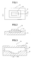
- FIGS. 1 and 2 show the first preferred embodiment of a metal/ceramic bonding substrate according to the present invention.
- the metal/ceramic bonding substrate 10 in this preferred embodiment comprises a substantially rectangular flat-plate-shaped ceramic substrate 12, at least one (only one is shown in FIGS. 1 and 2) substantially rectangular flat-plate-shaped circuit forming metal plate 14 which is bonded to one side of the ceramic substrate 12 and which is smaller than the ceramic substrate 12, and a radiating metal base plate 16 which is bonded to the other side of the ceramic substrate 12 and which has a substantially rectangular planar shape.
- the ceramic substrate 12 is embedded in the metal base plate 16 by about half the thickness of the ceramic substrate 12, so as to be arranged in parallel to the metal base plate 16 to allow the metal plate 14 to be spaced from the metal base plate 16 by a predetermined distance.
- the metal/ceramic bonding substrate 10 in this preferred embodiment may be produced by, e.g., a method comprising the steps of: preparing a mold 20 shown in FIG. 3; arranging the ceramic substrate 12 in the mold 20; injecting a molten metal into the mold 20 so as to contact both sides of the ceramic substrate 12; and thereafter, cooling and solidifying the molten metal to bond the circuit forming metal plate 14 to one side of the ceramic substrate 12 and to bond the radiating metal base plate 16 to the other side thereof.
- the mold 20 comprises lower and upper mold members 22 and 24 which have a substantially rectangular planar shape and which are made of a gas permeable material, such as carbon or a porous metal.
- a gas permeable material such as carbon or a porous metal.
- a recessed portion serving as a ceramic substrate holding portion 22a which substantially has the same planar shape and area as those of the ceramic substrate 12 and which has a depth about half the thickness of the ceramic substrate 12.
- a recessed portion serving as a metal circuit plate forming portion 22b which substantially has the same shape and size as those of the circuit forming metal plate 14.
- a metal base plate forming portion 24a which substantially has the same shape and size as those of the radiating metal base plate 16. Furthermore, a molten metal inlet (not shown) for injecting a molten metal into the mold 20 is formed in the upper mold member 24. In the lower mold member 22, a molten metal passage (not shown) extending between the metal base plate forming portion 24a and the metal circuit plate forming portion 22b is formed so as to allow the metal base plate forming portion 24a to be communicated with the metal circuit plate forming portion 22b if the ceramic substrate 12 is housed in the ceramic substrate holding portion 22a.
- the upper mold member 24 is arranged thereon to be fixed thereto. Thereafter, a molten metal, such as molten aluminum, is injected into the metal base plate forming portion 24a to be filled in the metal circuit plate forming portion 22b via the moltenmetalpassage. Then, the molten metal is cooled to be solidified to obtain a metal/ceramic bonding substrate 10 shown in FIGS. 1 and 2.
- a molten metal such as molten aluminum
- FIG. 4 shows the second preferred embodiment of a metal/ceramic bonding substrate according to the present invention.
- the metal/ceramic bonding substrate 110 in this preferred embodiment comprises a substantially rectangular flat-plate-shaped ceramic substrate 112, at least one (only one is shown in FIG. 4) substantially rectangular flat-plate-shaped circuit forming metal plate 114 which is bonded to one side of the ceramic substrate 112 and which is smaller than the ceramic substrate 112, and a radiating metal base plate 116 which is bonded to the other side of the ceramic substrate 112 and which has a substantially rectangular planar shape.
- the ceramic substrate 112 is embedded in the metal base plate 16 by the entire thickness thereof, so as to be arranged in parallel to the metal base plate 116 to allow the metal plate 114 to be spaced from the metal base plate 116 by a predetermined distance.
- the plane of the ceramic substrate 112 on the side of the metal plate 114 is the same plane as the exposed surface of the metal base plate 116 on the side of the metal plate 114.
- the metal/ceramic bonding substrate 110 in this preferred embodiment may be produced by, e.g., a method comprising the steps of: preparing a mold 120 shown in FIG. 5; arranging the ceramic substrate 112 in the mold 120; injecting a molten metal into the mold 120 so as to contact both sides of the ceramic substrate 112; and thereafter, cooling and solidifying the molten metal to bond the circuit forming metal plate 114 to one side of the ceramic substrate 112 and to bond the radiating metal base plate 116 to the other side thereof.
- the mold 120 comprises lower and upper mold members 122 and 124 which have a substantially rectangular planar shape and which are made of a gas permeable material, such as carbon or a porous metal.
- a gas permeable material such as carbon or a porous metal.
- a recessed portion serving as a metal circuit plate forming portion 122b which substantially has the same shape and size as those of the circuit forming metal plate 114.
- the ceramic substrate 112 is designed to be arranged so as to cover the metal circuit plate forming portion 122b.
- the upper mold member 124 there is formed a metal base plate forming portion 124a which substantially has the same shape and size as those of the radiating metal base plate 116 in which the ceramic substrate 112 is to be embedded.
- a molten metal inlet (not shown) for injecting a molten metal into the mold 120 is formed in the upper mold member 124.
- a molten metal passage (not shown) extending between the metal base plate forming portion 124a and the metal circuit plate forming portion 122b is formed so as to allow the metal base plate forming portion 124a to be communicated with the metal circuit plate forming portion 122b if the ceramic substrate 112 is arranged so as to cover the metal circuit plate forming portion 122b.
- protrusions or ribs for positioning the ceramic substrate 112 may be formed on the top of the lower mold member 122 so as to correspond to the side faces of the ceramic substrate 112, so that the ceramic substrate 112 may be arranged in a region surrounded by the protrusions or ribs.
- the protrusions or ribs are preferably formed in portions corresponding to the substantially central portion of the side faces of the ceramic substrate 112, except for portions corresponding to the corner portions of the ceramic substrate 112, so that the corner portions of the ceramic substrate 112, in which cracks are easily produced after heat cycles, are covered with the radiating metal base plate 116.
- the upper mold member 124 is arranged on the lower mold member 122 to be fixed thereto. Thereafter, a molten metal, such as molten aluminum, is injected into the metal base plate forming portion 124a to be filled in the metal circuit plate forming portion 122b via the molten metal passage. Then, the molten metal is cooled to be solidified to obtain a metal/ceramic bonding substrate 110 shown in FIG. 4.
- a molten metal such as molten aluminum
- the metal/ceramic bonding substrate thus produced in the first or second preferred embodiment can be used as a ceramic circuit board for a power module or as a semiconductor mounting ceramic circuit board after a circuit pattern is formed on the circuit forming metal plate.
- a metal/ceramic bonding circuit board thus produced can be used for producing a power module reliable to heat cycles, by assembling steps of soldering semiconductor chips such as Si chips, wiring by wire bonding of aluminum or the like, bonding a plastic package, and so forth.
- a metal/ceramic bonding substrate according to the present invention may be produced by another method, such as the braz ing and soldering method or the direct bonding method.
- a plurality of ceramic substrates may be bonded to the radiating metal base plate according to the present invention.
- the shape of the radiatingmetal base plate has been the substantially flat plate shape and the opposite surface (reverse) of the radiating metal base plate to the ceramic substrate has been flat in the above described first and second preferred embodiments
- a base plate having fins on its reverse, or a water cooling base plate including a water cooling channel may be used as the radiating metal base plate.
- Such a metal base plate can be also used for obtaining the same advantageous effects as those in the above described first and second preferred embodiments.
- the single circuit forming metal plate has been illustrated in the above described first and second preferred embodiments, the same advantageous effects can be obtained even if a plurality of circuit forming metal plates are used.
- a smooth rising portion or a stepped rising portion may be formed on the surface of the radiating metal base plate on the side of the metal plate so as to surround the ceramic substrate to be bonded to part or all of each side face of the ceramic substrate as shown in FIGS. 6 through 9. If at least part of each side face of the ceramic substrate is thus bonded to the radiating metal base plate, it is possible to obtain the same advantageous effects as those in the above described first and second preferred embodiments.
- reference numbers 210, 310, 410 and 510 denote a metal/ceramic bonding substrate
- reference numbers 212, 312, 412 and 512 denote a ceramic substrate.
- reference numbers 214, 314, 414 and 514 denote a circuit forming metal plate
- reference numbers 216, 316, 416 and 516 denote a radiating metal base plate.
Landscapes
- Cooling Or The Like Of Semiconductors Or Solid State Devices (AREA)
- Ceramic Products (AREA)
- Insulated Metal Substrates For Printed Circuits (AREA)
Applications Claiming Priority (2)
| Application Number | Priority Date | Filing Date | Title |
|---|---|---|---|
| JP2003360846 | 2003-10-21 | ||
| JP2003360846A JP4806803B2 (ja) | 2003-10-21 | 2003-10-21 | 金属−セラミックス接合基板およびその製造方法 |
Publications (3)
| Publication Number | Publication Date |
|---|---|
| EP1526569A2 true EP1526569A2 (de) | 2005-04-27 |
| EP1526569A3 EP1526569A3 (de) | 2007-07-18 |
| EP1526569B1 EP1526569B1 (de) | 2019-10-02 |
Family
ID=34386480
Family Applications (1)
| Application Number | Title | Priority Date | Filing Date |
|---|---|---|---|
| EP04024974.0A Expired - Lifetime EP1526569B1 (de) | 2003-10-21 | 2004-10-20 | Metallkeramiksubstrat und seine Herstellungsmethode |
Country Status (3)
| Country | Link |
|---|---|
| US (1) | US7122243B2 (de) |
| EP (1) | EP1526569B1 (de) |
| JP (1) | JP4806803B2 (de) |
Families Citing this family (12)
| Publication number | Priority date | Publication date | Assignee | Title |
|---|---|---|---|---|
| JP4543279B2 (ja) * | 2004-03-31 | 2010-09-15 | Dowaメタルテック株式会社 | アルミニウム接合部材の製造方法 |
| JP2007294891A (ja) * | 2006-03-30 | 2007-11-08 | Dowa Metaltech Kk | 放熱器 |
| WO2008123172A1 (ja) * | 2007-03-27 | 2008-10-16 | Ngk Insulators, Ltd. | ヒートスプレッダモジュール、ヒートシンク及びそれらの製法 |
| JP2008283067A (ja) * | 2007-05-11 | 2008-11-20 | Denso Corp | Al−AlN複合材料及びその製造方法並びに熱交換器 |
| JP2012142371A (ja) * | 2010-12-28 | 2012-07-26 | Mitsubishi Electric Corp | 半導体パッケージ |
| KR101255944B1 (ko) * | 2011-07-20 | 2013-04-23 | 삼성전기주식회사 | 전력 모듈 패키지용 기판 및 그 제조방법 |
| CN106102329B (zh) * | 2016-08-22 | 2019-07-26 | 景旺电子科技(龙川)有限公司 | 一种嵌陶瓷片金属基印制电路板制作方法 |
| JP6769541B2 (ja) * | 2017-02-23 | 2020-10-14 | 三菱電機株式会社 | 半導体装置 |
| JP7659377B2 (ja) * | 2020-09-15 | 2025-04-09 | Dowaメタルテック株式会社 | 放熱部材およびその製造方法 |
| CN116711072A (zh) * | 2021-01-22 | 2023-09-05 | 三菱电机株式会社 | 半导体装置及半导体装置的制造方法 |
| TWI790671B (zh) * | 2021-07-04 | 2023-01-21 | 郭明騰 | 光源模組 |
| CN118175729B (zh) * | 2024-05-15 | 2024-08-27 | 浙江万正电子科技股份有限公司 | 一种高散热嵌氮化铝pcb基板及其制作方法 |
Family Cites Families (16)
| Publication number | Priority date | Publication date | Assignee | Title |
|---|---|---|---|---|
| JPS63271944A (ja) * | 1987-04-28 | 1988-11-09 | Sumitomo Electric Ind Ltd | 半導体装置 |
| JP2504610B2 (ja) * | 1990-07-26 | 1996-06-05 | 株式会社東芝 | 電力用半導体装置 |
| US5570502A (en) * | 1991-04-08 | 1996-11-05 | Aluminum Company Of America | Fabricating metal matrix composites containing electrical insulators |
| US5602720A (en) * | 1993-06-25 | 1997-02-11 | Sumitomo Electric Industries, Ltd. | Mounting structure for semiconductor device having low thermal resistance |
| US5965193A (en) * | 1994-04-11 | 1999-10-12 | Dowa Mining Co., Ltd. | Process for preparing a ceramic electronic circuit board and process for preparing aluminum or aluminum alloy bonded ceramic material |
| JPH08191120A (ja) * | 1995-01-10 | 1996-07-23 | Hitachi Ltd | パワー半導体素子用基板とその製造方法 |
| JPH08330507A (ja) * | 1995-05-30 | 1996-12-13 | Motorola Inc | ハイブリッド・マルチチップ・モデュールおよびその製造方法 |
| JP3635379B2 (ja) * | 1995-08-04 | 2005-04-06 | 同和鉱業株式会社 | 金属−セラミックス複合基板 |
| EP0874399A1 (de) * | 1996-08-20 | 1998-10-28 | Kabushiki Kaisha Toshiba | Siliziumnitrid-leiterplatte und halbleiter-modul |
| US5944097A (en) * | 1997-05-06 | 1999-08-31 | Northrop Grumman Corporation | Composite substrate carrier for high power electronic devices |
| US6245442B1 (en) * | 1997-05-28 | 2001-06-12 | Kabushiki Kaisha Toyota Chuo | Metal matrix composite casting and manufacturing method thereof |
| JP3449683B2 (ja) * | 1997-12-01 | 2003-09-22 | 電気化学工業株式会社 | セラミックス回路基板とその製造方法 |
| JP4756200B2 (ja) | 2000-09-04 | 2011-08-24 | Dowaメタルテック株式会社 | 金属セラミックス回路基板 |
| JP2003229531A (ja) * | 2002-02-05 | 2003-08-15 | Sanyo Electric Co Ltd | 混成集積回路装置およびその製造方法 |
| JP4133170B2 (ja) * | 2002-09-27 | 2008-08-13 | Dowaホールディングス株式会社 | アルミニウム−セラミックス接合体 |
| US6933443B2 (en) * | 2004-01-28 | 2005-08-23 | Infineon Technologies North America Corp. | Method for bonding ceramic to copper, without creating a bow in the copper |
-
2003
- 2003-10-21 JP JP2003360846A patent/JP4806803B2/ja not_active Expired - Fee Related
-
2004
- 2004-10-19 US US10/969,360 patent/US7122243B2/en not_active Expired - Lifetime
- 2004-10-20 EP EP04024974.0A patent/EP1526569B1/de not_active Expired - Lifetime
Non-Patent Citations (1)
| Title |
|---|
| None |
Also Published As
| Publication number | Publication date |
|---|---|
| US7122243B2 (en) | 2006-10-17 |
| JP4806803B2 (ja) | 2011-11-02 |
| EP1526569B1 (de) | 2019-10-02 |
| EP1526569A3 (de) | 2007-07-18 |
| JP2005129577A (ja) | 2005-05-19 |
| US20050084704A1 (en) | 2005-04-21 |
Similar Documents
| Publication | Publication Date | Title |
|---|---|---|
| US8039757B2 (en) | Electronic part mounting substrate and method for producing same | |
| US8745841B2 (en) | Aluminum bonding member and method for producing same | |
| US7122243B2 (en) | Metal/ceramic bonding substrate and method for producing same | |
| US8283762B2 (en) | Lead frame based semiconductor package and a method of manufacturing the same | |
| US11291146B2 (en) | Leadframe substrate having modulator and crack inhibiting structure and flip chip assembly using the same | |
| JP5837754B2 (ja) | 金属−セラミックス接合基板およびその製造方法 | |
| US7189449B2 (en) | Metal/ceramic bonding substrate and method for producing same | |
| JP4722415B2 (ja) | 半導体装置およびその製造方法 | |
| JP5619437B2 (ja) | 金属−セラミックス接合基板の製造方法 | |
| CN110047811A (zh) | 线路基板、堆叠式半导体组件及其制作方法 | |
| JP4565249B2 (ja) | 金属−セラミックス接合基板およびその製造方法 | |
| US7255931B2 (en) | Aluminum/ceramic bonding substrate and method for producing same | |
| JP5389595B2 (ja) | 金属−セラミックス接合基板及びその製造方法 | |
| EP4131361A1 (de) | Keramische leiterplatte, wärmeableitendes element und aluminium-diamant-komplex | |
| JP2010034560A (ja) | 半導体モジュール、および電子回路を製造するための方法 | |
| JP7422608B2 (ja) | 金属-セラミックス接合基板およびその製造方法 | |
| JP7601261B2 (ja) | 半導体装置及びその製造方法 | |
| US6698088B2 (en) | Universal clamping mechanism | |
| JP2022157227A (ja) | 金属-セラミックス接合基板およびその製造方法 | |
| JP2020132477A (ja) | 金属−セラミックス接合基板およびその製造方法 |
Legal Events
| Date | Code | Title | Description |
|---|---|---|---|
| PUAI | Public reference made under article 153(3) epc to a published international application that has entered the european phase |
Free format text: ORIGINAL CODE: 0009012 |
|
| AK | Designated contracting states |
Kind code of ref document: A2 Designated state(s): AT BE BG CH CY CZ DE DK EE ES FI FR GB GR HU IE IT LI LU MC NL PL PT RO SE SI SK TR |
|
| AX | Request for extension of the european patent |
Extension state: AL HR LT LV MK |
|
| PUAL | Search report despatched |
Free format text: ORIGINAL CODE: 0009013 |
|
| AK | Designated contracting states |
Kind code of ref document: A3 Designated state(s): AT BE BG CH CY CZ DE DK EE ES FI FR GB GR HU IE IT LI LU MC NL PL PT RO SE SI SK TR |
|
| AX | Request for extension of the european patent |
Extension state: AL HR LT LV MK |
|
| RAP1 | Party data changed (applicant data changed or rights of an application transferred) |
Owner name: DOWA HOLDINGS CO., LTD. |
|
| RAP1 | Party data changed (applicant data changed or rights of an application transferred) |
Owner name: DOWA METALTECH CO., LTD. |
|
| 17P | Request for examination filed |
Effective date: 20071106 |
|
| 17Q | First examination report despatched |
Effective date: 20071220 |
|
| AKX | Designation fees paid |
Designated state(s): DE |
|
| RIC1 | Information provided on ipc code assigned before grant |
Ipc: H01L 23/14 20060101ALI20190220BHEP Ipc: H01L 23/15 20060101AFI20190220BHEP Ipc: H01L 23/13 20060101ALI20190220BHEP Ipc: H01L 23/373 20060101ALI20190220BHEP |
|
| GRAP | Despatch of communication of intention to grant a patent |
Free format text: ORIGINAL CODE: EPIDOSNIGR1 |
|
| INTG | Intention to grant announced |
Effective date: 20190415 |
|
| GRAS | Grant fee paid |
Free format text: ORIGINAL CODE: EPIDOSNIGR3 |
|
| GRAA | (expected) grant |
Free format text: ORIGINAL CODE: 0009210 |
|
| AK | Designated contracting states |
Kind code of ref document: B1 Designated state(s): DE |
|
| RIN1 | Information on inventor provided before grant (corrected) |
Inventor name: OSANAI, HIDEYO Inventor name: NAMIOKA, MAKOTO Inventor name: TAKAHASHI, TAKAYUKI |
|
| REG | Reference to a national code |
Ref country code: DE Ref legal event code: R096 Ref document number: 602004054272 Country of ref document: DE |
|
| REG | Reference to a national code |
Ref country code: DE Ref legal event code: R097 Ref document number: 602004054272 Country of ref document: DE |
|
| PLBE | No opposition filed within time limit |
Free format text: ORIGINAL CODE: 0009261 |
|
| STAA | Information on the status of an ep patent application or granted ep patent |
Free format text: STATUS: NO OPPOSITION FILED WITHIN TIME LIMIT |
|
| 26N | No opposition filed |
Effective date: 20200703 |
|
| PGFP | Annual fee paid to national office [announced via postgrant information from national office to epo] |
Ref country code: DE Payment date: 20230830 Year of fee payment: 20 |
|
| REG | Reference to a national code |
Ref country code: DE Ref legal event code: R071 Ref document number: 602004054272 Country of ref document: DE |