EP1526584A2 - Nanocristaux semiconducteurs photosensitifs, compose comprenant de nanocristaux semiconducteurs photosensitifs et méthode de fabrication des structures nanocristallines semiconductrices photosensitives en les utilisant - Google Patents
Nanocristaux semiconducteurs photosensitifs, compose comprenant de nanocristaux semiconducteurs photosensitifs et méthode de fabrication des structures nanocristallines semiconductrices photosensitives en les utilisant Download PDFInfo
- Publication number
- EP1526584A2 EP1526584A2 EP20040256185 EP04256185A EP1526584A2 EP 1526584 A2 EP1526584 A2 EP 1526584A2 EP 20040256185 EP20040256185 EP 20040256185 EP 04256185 A EP04256185 A EP 04256185A EP 1526584 A2 EP1526584 A2 EP 1526584A2
- Authority
- EP
- European Patent Office
- Prior art keywords
- acid
- group
- nanocrystals
- trans
- diacrylate
- Prior art date
- Legal status (The legal status is an assumption and is not a legal conclusion. Google has not performed a legal analysis and makes no representation as to the accuracy of the status listed.)
- Granted
Links
Images



Classifications
-
- G—PHYSICS
- G03—PHOTOGRAPHY; CINEMATOGRAPHY; ANALOGOUS TECHNIQUES USING WAVES OTHER THAN OPTICAL WAVES; ELECTROGRAPHY; HOLOGRAPHY
- G03F—PHOTOMECHANICAL PRODUCTION OF TEXTURED OR PATTERNED SURFACES, e.g. FOR PRINTING, FOR PROCESSING OF SEMICONDUCTOR DEVICES; MATERIALS THEREFOR; ORIGINALS THEREFOR; APPARATUS SPECIALLY ADAPTED THEREFOR
- G03F7/00—Photomechanical, e.g. photolithographic, production of textured or patterned surfaces, e.g. printing surfaces; Materials therefor, e.g. comprising photoresists; Apparatus specially adapted therefor
-
- B—PERFORMING OPERATIONS; TRANSPORTING
- B82—NANOTECHNOLOGY
- B82B—NANOSTRUCTURES FORMED BY MANIPULATION OF INDIVIDUAL ATOMS, MOLECULES, OR LIMITED COLLECTIONS OF ATOMS OR MOLECULES AS DISCRETE UNITS; MANUFACTURE OR TREATMENT THEREOF
- B82B1/00—Nanostructures formed by manipulation of individual atoms or molecules, or limited collections of atoms or molecules as discrete units
-
- B—PERFORMING OPERATIONS; TRANSPORTING
- B82—NANOTECHNOLOGY
- B82B—NANOSTRUCTURES FORMED BY MANIPULATION OF INDIVIDUAL ATOMS, MOLECULES, OR LIMITED COLLECTIONS OF ATOMS OR MOLECULES AS DISCRETE UNITS; MANUFACTURE OR TREATMENT THEREOF
- B82B3/00—Manufacture or treatment of nanostructures by manipulation of individual atoms or molecules, or limited collections of atoms or molecules as discrete units
-
- B—PERFORMING OPERATIONS; TRANSPORTING
- B82—NANOTECHNOLOGY
- B82Y—SPECIFIC USES OR APPLICATIONS OF NANOSTRUCTURES; MEASUREMENT OR ANALYSIS OF NANOSTRUCTURES; MANUFACTURE OR TREATMENT OF NANOSTRUCTURES
- B82Y20/00—Nanooptics, e.g. quantum optics or photonic crystals
-
- B—PERFORMING OPERATIONS; TRANSPORTING
- B82—NANOTECHNOLOGY
- B82Y—SPECIFIC USES OR APPLICATIONS OF NANOSTRUCTURES; MEASUREMENT OR ANALYSIS OF NANOSTRUCTURES; MANUFACTURE OR TREATMENT OF NANOSTRUCTURES
- B82Y30/00—Nanotechnology for materials or surface science, e.g. nanocomposites
-
- C—CHEMISTRY; METALLURGY
- C08—ORGANIC MACROMOLECULAR COMPOUNDS; THEIR PREPARATION OR CHEMICAL WORKING-UP; COMPOSITIONS BASED THEREON
- C08F—MACROMOLECULAR COMPOUNDS OBTAINED BY REACTIONS ONLY INVOLVING CARBON-TO-CARBON UNSATURATED BONDS
- C08F2/00—Processes of polymerisation
- C08F2/12—Polymerisation in non-solvents
- C08F2/16—Aqueous medium
- C08F2/22—Emulsion polymerisation
- C08F2/24—Emulsion polymerisation with the aid of emulsifying agents
- C08F2/28—Emulsion polymerisation with the aid of emulsifying agents cationic
-
- C—CHEMISTRY; METALLURGY
- C30—CRYSTAL GROWTH
- C30B—SINGLE-CRYSTAL GROWTH; UNIDIRECTIONAL SOLIDIFICATION OF EUTECTIC MATERIAL OR UNIDIRECTIONAL DEMIXING OF EUTECTOID MATERIAL; REFINING BY ZONE-MELTING OF MATERIAL; PRODUCTION OF A HOMOGENEOUS POLYCRYSTALLINE MATERIAL WITH DEFINED STRUCTURE; SINGLE CRYSTALS OR HOMOGENEOUS POLYCRYSTALLINE MATERIAL WITH DEFINED STRUCTURE; AFTER-TREATMENT OF SINGLE CRYSTALS OR A HOMOGENEOUS POLYCRYSTALLINE MATERIAL WITH DEFINED STRUCTURE; APPARATUS THEREFOR
- C30B29/00—Single crystals or homogeneous polycrystalline material with defined structure characterised by the material or by their shape
- C30B29/60—Single crystals or homogeneous polycrystalline material with defined structure characterised by the material or by their shape characterised by shape
-
- C—CHEMISTRY; METALLURGY
- C30—CRYSTAL GROWTH
- C30B—SINGLE-CRYSTAL GROWTH; UNIDIRECTIONAL SOLIDIFICATION OF EUTECTIC MATERIAL OR UNIDIRECTIONAL DEMIXING OF EUTECTOID MATERIAL; REFINING BY ZONE-MELTING OF MATERIAL; PRODUCTION OF A HOMOGENEOUS POLYCRYSTALLINE MATERIAL WITH DEFINED STRUCTURE; SINGLE CRYSTALS OR HOMOGENEOUS POLYCRYSTALLINE MATERIAL WITH DEFINED STRUCTURE; AFTER-TREATMENT OF SINGLE CRYSTALS OR A HOMOGENEOUS POLYCRYSTALLINE MATERIAL WITH DEFINED STRUCTURE; APPARATUS THEREFOR
- C30B33/00—After-treatment of single crystals or homogeneous polycrystalline material with defined structure
-
- G—PHYSICS
- G03—PHOTOGRAPHY; CINEMATOGRAPHY; ANALOGOUS TECHNIQUES USING WAVES OTHER THAN OPTICAL WAVES; ELECTROGRAPHY; HOLOGRAPHY
- G03F—PHOTOMECHANICAL PRODUCTION OF TEXTURED OR PATTERNED SURFACES, e.g. FOR PRINTING, FOR PROCESSING OF SEMICONDUCTOR DEVICES; MATERIALS THEREFOR; ORIGINALS THEREFOR; APPARATUS SPECIALLY ADAPTED THEREFOR
- G03F7/00—Photomechanical, e.g. photolithographic, production of textured or patterned surfaces, e.g. printing surfaces; Materials therefor, e.g. comprising photoresists; Apparatus specially adapted therefor
- G03F7/004—Photosensitive materials
- G03F7/0042—Photosensitive materials with inorganic or organometallic light-sensitive compounds not otherwise provided for, e.g. inorganic resists
- G03F7/0043—Chalcogenides; Silicon, germanium, arsenic or derivatives thereof; Metals, oxides or alloys thereof
-
- G—PHYSICS
- G03—PHOTOGRAPHY; CINEMATOGRAPHY; ANALOGOUS TECHNIQUES USING WAVES OTHER THAN OPTICAL WAVES; ELECTROGRAPHY; HOLOGRAPHY
- G03F—PHOTOMECHANICAL PRODUCTION OF TEXTURED OR PATTERNED SURFACES, e.g. FOR PRINTING, FOR PROCESSING OF SEMICONDUCTOR DEVICES; MATERIALS THEREFOR; ORIGINALS THEREFOR; APPARATUS SPECIALLY ADAPTED THEREFOR
- G03F7/00—Photomechanical, e.g. photolithographic, production of textured or patterned surfaces, e.g. printing surfaces; Materials therefor, e.g. comprising photoresists; Apparatus specially adapted therefor
- G03F7/004—Photosensitive materials
- G03F7/0047—Photosensitive materials characterised by additives for obtaining a metallic or ceramic pattern, e.g. by firing
-
- H—ELECTRICITY
- H10—SEMICONDUCTOR DEVICES; ELECTRIC SOLID-STATE DEVICES NOT OTHERWISE PROVIDED FOR
- H10K—ORGANIC ELECTRIC SOLID-STATE DEVICES
- H10K50/00—Organic light-emitting devices
- H10K50/10—OLEDs or polymer light-emitting diodes [PLED]
- H10K50/11—OLEDs or polymer light-emitting diodes [PLED] characterised by the electroluminescent [EL] layers
- H10K50/115—OLEDs or polymer light-emitting diodes [PLED] characterised by the electroluminescent [EL] layers comprising active inorganic nanostructures, e.g. luminescent quantum dots
-
- G—PHYSICS
- G03—PHOTOGRAPHY; CINEMATOGRAPHY; ANALOGOUS TECHNIQUES USING WAVES OTHER THAN OPTICAL WAVES; ELECTROGRAPHY; HOLOGRAPHY
- G03F—PHOTOMECHANICAL PRODUCTION OF TEXTURED OR PATTERNED SURFACES, e.g. FOR PRINTING, FOR PROCESSING OF SEMICONDUCTOR DEVICES; MATERIALS THEREFOR; ORIGINALS THEREFOR; APPARATUS SPECIALLY ADAPTED THEREFOR
- G03F7/00—Photomechanical, e.g. photolithographic, production of textured or patterned surfaces, e.g. printing surfaces; Materials therefor, e.g. comprising photoresists; Apparatus specially adapted therefor
- G03F7/004—Photosensitive materials
- G03F7/027—Non-macromolecular photopolymerisable compounds having carbon-to-carbon double bonds, e.g. ethylenic compounds
-
- Y—GENERAL TAGGING OF NEW TECHNOLOGICAL DEVELOPMENTS; GENERAL TAGGING OF CROSS-SECTIONAL TECHNOLOGIES SPANNING OVER SEVERAL SECTIONS OF THE IPC; TECHNICAL SUBJECTS COVERED BY FORMER USPC CROSS-REFERENCE ART COLLECTIONS [XRACs] AND DIGESTS
- Y02—TECHNOLOGIES OR APPLICATIONS FOR MITIGATION OR ADAPTATION AGAINST CLIMATE CHANGE
- Y02E—REDUCTION OF GREENHOUSE GAS [GHG] EMISSIONS, RELATED TO ENERGY GENERATION, TRANSMISSION OR DISTRIBUTION
- Y02E10/00—Energy generation through renewable energy sources
- Y02E10/50—Photovoltaic [PV] energy
- Y02E10/549—Organic PV cells
-
- Y—GENERAL TAGGING OF NEW TECHNOLOGICAL DEVELOPMENTS; GENERAL TAGGING OF CROSS-SECTIONAL TECHNOLOGIES SPANNING OVER SEVERAL SECTIONS OF THE IPC; TECHNICAL SUBJECTS COVERED BY FORMER USPC CROSS-REFERENCE ART COLLECTIONS [XRACs] AND DIGESTS
- Y10—TECHNICAL SUBJECTS COVERED BY FORMER USPC
- Y10S—TECHNICAL SUBJECTS COVERED BY FORMER USPC CROSS-REFERENCE ART COLLECTIONS [XRACs] AND DIGESTS
- Y10S428/00—Stock material or miscellaneous articles
- Y10S428/917—Electroluminescent
-
- Y—GENERAL TAGGING OF NEW TECHNOLOGICAL DEVELOPMENTS; GENERAL TAGGING OF CROSS-SECTIONAL TECHNOLOGIES SPANNING OVER SEVERAL SECTIONS OF THE IPC; TECHNICAL SUBJECTS COVERED BY FORMER USPC CROSS-REFERENCE ART COLLECTIONS [XRACs] AND DIGESTS
- Y10—TECHNICAL SUBJECTS COVERED BY FORMER USPC
- Y10S—TECHNICAL SUBJECTS COVERED BY FORMER USPC CROSS-REFERENCE ART COLLECTIONS [XRACs] AND DIGESTS
- Y10S977/00—Nanotechnology
- Y10S977/70—Nanostructure
- Y10S977/773—Nanoparticle, i.e. structure having three dimensions of 100 nm or less
-
- Y—GENERAL TAGGING OF NEW TECHNOLOGICAL DEVELOPMENTS; GENERAL TAGGING OF CROSS-SECTIONAL TECHNOLOGIES SPANNING OVER SEVERAL SECTIONS OF THE IPC; TECHNICAL SUBJECTS COVERED BY FORMER USPC CROSS-REFERENCE ART COLLECTIONS [XRACs] AND DIGESTS
- Y10—TECHNICAL SUBJECTS COVERED BY FORMER USPC
- Y10T—TECHNICAL SUBJECTS COVERED BY FORMER US CLASSIFICATION
- Y10T428/00—Stock material or miscellaneous articles
- Y10T428/24—Structurally defined web or sheet [e.g., overall dimension, etc.]
- Y10T428/24802—Discontinuous or differential coating, impregnation or bond [e.g., artwork, printing, retouched photograph, etc.]
-
- Y—GENERAL TAGGING OF NEW TECHNOLOGICAL DEVELOPMENTS; GENERAL TAGGING OF CROSS-SECTIONAL TECHNOLOGIES SPANNING OVER SEVERAL SECTIONS OF THE IPC; TECHNICAL SUBJECTS COVERED BY FORMER USPC CROSS-REFERENCE ART COLLECTIONS [XRACs] AND DIGESTS
- Y10—TECHNICAL SUBJECTS COVERED BY FORMER USPC
- Y10T—TECHNICAL SUBJECTS COVERED BY FORMER US CLASSIFICATION
- Y10T428/00—Stock material or miscellaneous articles
- Y10T428/26—Web or sheet containing structurally defined element or component, the element or component having a specified physical dimension
- Y10T428/263—Coating layer not in excess of 5 mils thick or equivalent
- Y10T428/264—Up to 3 mils
- Y10T428/265—1 mil or less
-
- Y—GENERAL TAGGING OF NEW TECHNOLOGICAL DEVELOPMENTS; GENERAL TAGGING OF CROSS-SECTIONAL TECHNOLOGIES SPANNING OVER SEVERAL SECTIONS OF THE IPC; TECHNICAL SUBJECTS COVERED BY FORMER USPC CROSS-REFERENCE ART COLLECTIONS [XRACs] AND DIGESTS
- Y10—TECHNICAL SUBJECTS COVERED BY FORMER USPC
- Y10T—TECHNICAL SUBJECTS COVERED BY FORMER US CLASSIFICATION
- Y10T428/00—Stock material or miscellaneous articles
- Y10T428/29—Coated or structually defined flake, particle, cell, strand, strand portion, rod, filament, macroscopic fiber or mass thereof
- Y10T428/2982—Particulate matter [e.g., sphere, flake, etc.]
- Y10T428/2991—Coated
-
- Y—GENERAL TAGGING OF NEW TECHNOLOGICAL DEVELOPMENTS; GENERAL TAGGING OF CROSS-SECTIONAL TECHNOLOGIES SPANNING OVER SEVERAL SECTIONS OF THE IPC; TECHNICAL SUBJECTS COVERED BY FORMER USPC CROSS-REFERENCE ART COLLECTIONS [XRACs] AND DIGESTS
- Y10—TECHNICAL SUBJECTS COVERED BY FORMER USPC
- Y10T—TECHNICAL SUBJECTS COVERED BY FORMER US CLASSIFICATION
- Y10T428/00—Stock material or miscellaneous articles
- Y10T428/29—Coated or structually defined flake, particle, cell, strand, strand portion, rod, filament, macroscopic fiber or mass thereof
- Y10T428/2982—Particulate matter [e.g., sphere, flake, etc.]
- Y10T428/2991—Coated
- Y10T428/2998—Coated including synthetic resin or polymer
-
- Y—GENERAL TAGGING OF NEW TECHNOLOGICAL DEVELOPMENTS; GENERAL TAGGING OF CROSS-SECTIONAL TECHNOLOGIES SPANNING OVER SEVERAL SECTIONS OF THE IPC; TECHNICAL SUBJECTS COVERED BY FORMER USPC CROSS-REFERENCE ART COLLECTIONS [XRACs] AND DIGESTS
- Y10—TECHNICAL SUBJECTS COVERED BY FORMER USPC
- Y10T—TECHNICAL SUBJECTS COVERED BY FORMER US CLASSIFICATION
- Y10T428/00—Stock material or miscellaneous articles
- Y10T428/31504—Composite [nonstructural laminate]
-
- Y—GENERAL TAGGING OF NEW TECHNOLOGICAL DEVELOPMENTS; GENERAL TAGGING OF CROSS-SECTIONAL TECHNOLOGIES SPANNING OVER SEVERAL SECTIONS OF THE IPC; TECHNICAL SUBJECTS COVERED BY FORMER USPC CROSS-REFERENCE ART COLLECTIONS [XRACs] AND DIGESTS
- Y10—TECHNICAL SUBJECTS COVERED BY FORMER USPC
- Y10T—TECHNICAL SUBJECTS COVERED BY FORMER US CLASSIFICATION
- Y10T428/00—Stock material or miscellaneous articles
- Y10T428/31504—Composite [nonstructural laminate]
- Y10T428/31652—Of asbestos
- Y10T428/31663—As siloxane, silicone or silane
Definitions
- the present invention relates to photosensitive semiconductor nanocrystals, a photosensitive composition comprising semiconductor nanocrystals and a method for forming a semiconductor nanocrystal pattern using the same. More particularly, the present invention relates to semiconductor nanocrystals that are surface-coordinated with a compound containing a photosensitive functional group, a photosensitive composition comprising semiconductor nanocrystals, and a method for forming a semiconductor nanocrystal pattern by forming a film using the photosensitive semiconductor nanocrystals or the photosensitive composition, exposing the film to light and developing the exposed film.
- the wet chemistry method has an advantage in that nanocrystals can be uniformly synthesized in various sizes by appropriately controlling the concentration of precursors used, the kind of organic solvents, synthesizing temperature and time, etc.
- nanocrystals prepared by the wet chemistry method are commonly dispersed in an organic solvent, such as toluene or chloroform
- an organic solvent such as toluene or chloroform
- techniques of forming a thin film as well as pattern forming method of nanocrystals are required in order to apply the nanocrystals to electronic devices.
- Patterning techniques reported hitherto are mainly associated with the patterning of nanocrystals by vapor deposition. These techniques, however, have a shortcoming in that control over the uniformity of size, shape, and density is difficult (Appl. Phys. Letter, 1997, 70, 3140).
- U.S. Patent No. 5,559,057 suggests a method for forming a pattern of nanocrystals which comprises the steps of vapor-depositing or spraying nanocrystals using a mask to deposit nanocrystals only on the areas not covered with a mask, irradiating the nanocrystals with an electron beam to produce a thin film, and removing the mask.
- U.S. Patent No. 6,139,626 discloses a method for indirectly forming a pattern of nanocrystals by filling in pores of a template with nanocrystals wherein the template may be patterned in any configuration.
- these patterning methods involve the use of a high-energy electron beam and a troublesome lift-off operation of the mask used.
- the template material may affect the performances of the pattern to be formed, and there is thus a limitation in the kind of materials that can be patterned.
- U.S. Patent. No. 5,751,018 discloses a method for aligning nanocrystals using terminal groups of a self-assembled monolayer formed on a metal substrate.
- U.S. Patent No. 6,602,671 describes a method for binding dispersed nanocrystals to a polymeric support. Since the above-mentioned methods are not substantially associated with patterning, they have limited applicability to the patterning of nanocrystals.
- a feature of the present invention is to provide novel photosensitive semiconductor nanocrystals for forming a semiconductor nanocrystal pattern.
- Another feature of the present invention is to provide a novel photosensitive composition comprising semiconductor nanocrystals for forming a semiconductor nanocrystal pattern.
- Still another feature of the present invention is to provide a method for forming a semiconductor nanocrystal pattern using the above photosensitive semiconductor nanocrystals and the photosensitive composition.
- semiconductor nanocrystals surface-coordinated with a compound containing a photosensitive functional group.
- a photosensitive composition for a semiconductor nanocrystal pattern comprising i) semiconductor nanocrystals, and ii) a photocurable compound.
- a method for forming a semiconductor nanocrystal pattern comprising the steps of: i) producing a semiconductor nanocrystal film using the above semiconductor nanocrystals or the above photosensitive composition; ii) exposing the film through a mask; and iii) developing the exposed film.
- an organic-inorganic hybrid electroluminescent device wherein the semiconductor nanocrystal pattern prepared according to the above method is contained as a luminescent layer.
- the photosensitive semiconductor nanocrystals of the present invention are semiconductor nanocrystals surface-coordinated with a compound containing a photosensitive functional group.
- Semiconductor nanocrystals usable in the present invention may include all semiconductor nanocrystals prepared from metal precursors by a wet chemistry method.
- the semiconductor nanocrystals may be prepared by adding a corresponding metal precursor to an organic solvent in the absence or presence of a dispersant, and growing crystals at a predetermined temperature.
- suitable semiconductor nanocrystals usable in the present invention include Group II-IV, III-IV and V compound nanocrystals and mixtures thereof.
- nanocrystals include, but are not limited to, CdS, CdSe, CdTe, ZnS, ZnSe, ZnTe, HgS, HgSe, HgTe, GaN, GaP, GaAs, InP, InAs and mixtures thereof. If the semiconductor nanocrystals are composed of two or more compounds, it may be a uniformly mixed type, gradiently mixed type, core-shell type or alloy type.
- the photosensitive compound coordinated to the surface of the semiconductor nanocrystals is a compound wherein a photoreactive functional group (e.g., carbon-carbon double bond or acryl group) is selectively bonded to a linker (e.g., cyanide, thiol (SH), amino, carboxylic acid group or phosphonic acid group).
- a linker e.g., cyanide, thiol (SH), amino, carboxylic acid group or phosphonic acid group.
- linker e.g., cyanide, thiol (SH), amino, carboxylic acid group or phosphonic acid group.
- the photosensitive compound is represented by Formula 1 below: X-A-B wherein X is NC-, HOOC-, HRN-, POOOH-, RS- or RSS- (in which R is a hydrogen atom or a C 1-10 saturated or unsaturated aliphatic hydrocarbon group); A is a direct bond, an aliphatic organic group, a phenylene group or a biphenylene group; and B is an organic group containing at least one carbon-carbon double bond, which may be substituted with at least one group selected from the group consisting of -CN, -COOH, halogen groups, C 1-5 halogenated alkyl groups, amine groups, C 6-15 aromatic hydrocarbon groups, and C 6-12 aromatic hydrocarbon groups substituted with F, Cl, Br, a halogenated alkyl group, R'O- (in which R' is a hydrogen atom or a C 1-5 alkyl group), -COOH, an amine group or -NO 2 .
- X is NC-
- the aliphatic organic group in the substituent A of Formula 1 is a saturated aliphatic hydrocarbon group such as -(CR 2 ) n - (in which R is a hydrogen atom, a C 1-5 alkyl group, and n is an integer of 1-30), an aliphatic ester group containing an ester moiety (-COO-), an aliphatic amide group containing an amide moiety (-NHCO-), an aliphatic oxycarbonyl group containing an oxycarbonyl moiety (-OCO-), or an aliphatic ether group containing an ether moiety (-O-).
- the aliphatic organic group may be branched with a C 1-5 alkyl group, or may be substituted with by a hydroxyl, amine or thiol group.
- R 1 is a hydrogen atom, -COOH, a halogen group,
- the C 1-30 alkyl group and the C 2-30 unsaturated aliphatic hydrocarbon group containing at least one carbon-carbon double bond may be branched by an alkyl group, and if necessary, may be substituted with a hydroxyl group, a carboxyl group, etc.
- the number of the double bonds in the unsaturated aliphatic hydrocarbon group is not especially limited, but is preferably 3 or less.
- Preferred examples of the compound represented by Formula 1 include, but are not limited to, methacrylic acid, crotonic acid, vinylacetic acid, tiglic acid, 3,3-dimethylacrylic acid, trans-2-pentenoic acid, 4-pentenoic acid, trans-2-methyl-2-pentenoic acid, 2,2-dimethyl-4-pentenoic acid, trans-2-hexenoic acid, trans-3-hexenoic acid, 2-ethyl-2-hexenoic acid, 6-heptenoic acid, 2-octenoic acid, citronellic acid, undecylenic acid, myristoleic acid, palmitoleic acid, oleic acid, elaidic acid, cis-11-elcosenoic acid, euric acid, nervonic acid, trans-2,4-pentadienoic acid, 2,4-hexadienoic acid, 2,6-heptadienoic acid, geranic acid, linoleic acid
- the photosensitive semiconductor nanocrystals of the present invention can be prepared by obtaining nanocrystals from a corresponding metal precursor, dispersing the obtained nanocrystals in an organic solvent, and treating the dispersion with the photosensitive compound of Formula 1.
- the treatment with the photosensitive compound is not especially limited, but is preferably carried out by refluxing the dispersion of the nanocrystals in the presence of the photosensitive compound.
- the reflux conditions, including time and temperature, and the concentration of the photosensitive compound can be properly controlled according to the kind of the dispersing solvent, the nanocrystals and the photosensitive compound coordinated to the surface of the nanocrystals.
- nanocrystals are surface-coordinated with a dispersant having a reactive end group, such as mercaptopropanol, and then reacted with a photosensitive compound capable of reacting with the reactive end group of the dispersant, such as methacryloyl chloride, thereby producing nanocrystals surface-coordinated with the photosensitive compound.
- a dispersant having a reactive end group such as mercaptopropanol
- a photosensitive compound capable of reacting with the reactive end group of the dispersant, such as methacryloyl chloride
- semiconductor nanocrystals may be directly surface-coordinated with a photosensitive compound by adding a metal precursor into an organic solvent and growing crystals at the predetermined temperature in the presence of the photosensitive compound.
- the kind of organic solvent, the crystal-growth temperature and the concentration of the precursor can be appropriately varied according to the kind of the photosensitive compound, and the kind, size and shape of the desired semiconductor nanocrystals.
- FIG. 1 A preferred embodiment of the photosensitive semiconductor nanocrystals according to the present invention is schematically shown in Fig. 1.
- X is a linker binding the semiconductor nanocrystals to a photosensitive functional group such as aryl or vinyl group.
- the surface-coordinating rate of the photosensitive compound to the semiconductor nanocrystals can be appropriately controlled by changing the mixing ratio of the nanocrystals and the compound.
- the photosensitive composition of the present invention comprises i) semiconductor nanocrystals, and ii) a photocurable compound
- semiconductor nanocrystals As to the semiconductor nanocrystals, common semiconductor nanocrystals or photosensitive semiconductor nanocrystals according to the present invention may be used. Where photosensitive semiconductor nanocrystals of the present invention are used, it is advantageous that substitution with a compound containing a photosensitive functional group is unnecessary.
- the semiconductor nanocrystals contained in the photosensitive composition of the present invention are as described above.
- polymers containing at least one acryl and/or vinyl group and ether-based compounds can be used. More concretely, polymers containing at least one acryl and/or vinyl group include multifunctional acrylate-based compounds, multifunctional polyalkyleneoxide compounds and polysiloxanes containing at least one acryl and/or vinyl group.
- Preferred examples of the photocurable compound include, but are not limited to, allyloxylated cyclohexyl diacrylate, bis(acryloxy ethyl)hydroxyl isocyanurate, bis(acryloxy neopentylglycol) adipate, bisphenol A diacrylate, bisphenyl A dimethacrylate, 1,4-butanediol diacrylate, 1,4-butanediol dimethacrylate, 1,3-butyleneglycol diacrylate, 1,3-butyleneglycol dimethacrylate, dicyclopentanyl diacrylate, diethyleneglycol diacrylate, diethyleneglycol dimethacrylate, dipentaerythitol hexaacrylate, dipentaerythitol monohydroxy pentacrylate, ditrimethylolprpane tetraacrylate, ethyleneglycol dimethacrylate, glycerol methacrylate, 1,6-hexanediol
- composition ratio of i) the semiconductor nanocrystals and ii) the photocurable compound contained in the photosensitive composition of the present invention is not especially limited, and can be properly controlled depending on the photocurability (i.e. curing rate, state of a cured film, etc.), binding ability between the photosensitive compound and the nanocrystals, etc.
- a semiconductor nanocrystal pattern can be formed by a) forming a semiconductor nanocrystal film using the photosensitive semiconductor nanocrystals or the photosensitive composition according to the present invention; b) exposing the film through mask; and c) developing the exposed film.
- the semiconductor nanocrystal film is produced by dispersing the photosensitive semiconductor nanocrystals or the photosensitive composition according to the present invention in a suitable organic solvent, and coating the dispersion onto a substrate.
- a photoinitiator may be added to the organic solvent.
- the photosensitive semiconductor nanocrystals or the photosensitive composition according to the present invention may be cured without a photoinitiator. However, if necessary, a photoinitiator may be used to assist the crosslinking reaction.
- photoinitiators usable in the present invention include those capable of forming free radicals upon light irradiation, such as acetophenone-, benzoin-, benzophenone- and thioxantone-based photoinitiators.
- acetophenone-based initiator usable in the present invention examples include 4-phenoxy dichloroacetophenone, 4-t-butyl dichloroacetophenone, 4-t-butyl trichloroacetophenone, diethoxyacetophenone, 2-hydroxy-2-methyl-1-phenyl-propane-1-one, 1-(4-isopropylphenyl)-2-hydroxy-2-methyl-propane-1-one, 1-(4-dodecylphenyl)-2-hydroxy-2-methylpropane-1-one, 4-(2-hydroxyethoxy)-phenyl-(2-hydroxy-2-propyl)ketone, 1-hydroxy cyclohexyl phenyl ketone, 2-methyl-1-[4-(methylthio)phenyl]-2-morpholino-propane-1, and the like.
- benzoin-based photoinitiator examples include benzoin, benzoin methyl ether, benzoin ethyl ether, benzoin isopropyl ether, benzoin isobutyl ether, benzyl dimethyl ketal, etc.
- benzophenone-based photoinitiator examples include benzophenone, benzoyl benzoic acid, benzoyl benzoic acid methyl ester, 4-phenyl benzophenone, hydroxy benzophenone, 4-benzoyl-4'-methyl diphenyl sulphide, 3,3'-dimethyl-4-methoxy benzophenone and the like.
- An organic solvent used in this process is not especially limited, but preferably those capable of homogeneously dispersing nanocrystals and being easily removed after application are used. More preferably, DMF, 4-hydroxy-4-methyl-2-pentanone, ethylene glycol monoethyl ether, 2-methoxyethanol, chloroform, chlorobenzene, toluene, teterahydrofuran, dichloromethane, hexane, heptane, octane, nonane, decane or a mixture thereof is used.
- the application may be carried out by a spin coating, dip coating, spray coating or blade coating process, but is not especially limited thereto.
- the film thus obtained is dried at 30-300°C and preferably 40-120°C to evaporate the organic solvents ahead of light exposure.
- step b) the film is selectively exposed to an electromagnetic wave through a photomask having a desired pattern.
- a crosslinking reaction takes place through photosensitive functional groups or photocurable compounds in the exposed area.
- This crosslinking reaction enables the formation of a network structure of semiconductor nanocrystals, resulting in a solubility difference between the exposed and unexposed areas.
- development of the film with a developing agent enables the formation of a negative pattern of semiconductor nanocrystals.
- the light exposure may be carried out by a contact or non-contact exposure process.
- the exposure dose is not especially limited, and can be appropriately controlled according to the thickness of the film formed.
- the light exposure is carried out at an exposure dose of 50-850 mJ/cm 2 .
- a light source usable for the light exposure preferably has an effective wavelength range of 200-500nm, preferably 300-400nm, and has an energy range of 100-800W.
- step c) the exposed film is developed with an appropriate developing agent to form a semiconductor nanocrystal pattern.
- developing agents usable in the present invention include organic solvents, such as toluene and chloroform, weakly acidic solutions and weakly basic solutions, and pure water.
- the semiconductor nanocrystal pattern formed by the method of the present invention exhibits excellent luminescence characteristics, it can be utilized in a variety of fields, including semiconductor devices, e.g., displays, sensors and solar cells.
- the pattern is useful in forming the luminescent layer of an organic-inorganic hybrid electroluminescent device.
- the pattern When the pattern is used to form a luminescent layer, it preferably has a thickness of 5-100nm.
- organic layers are formed in an electron transport layer or a hole transport layer except luminescent layer.
- the organic electroluminescent device has a structure selected from anode/luminescent layer/cathode, anode/buffer layer/luminescent layer/cathode, anode/hole transport layer/luminescent layer/cathode, anode/buffer layer/hole transport layer/luminescent layer/cathode, anode/buffer layer/hole transport layer/luminescent layer/electron transport layer/cathode, and anode/buffer layer/hole transport layer/luminescent layer/hole blocking layer/cathode , but is not particularly limited to these structures.
- buffer layer materials compounds commonly used in the art for this purpose can be used.
- Preferred examples include, but are not limited to, copper phthalocyanine, polythiophene, polyaniline, polyacetylene, polypyrrole, polyphenylene vinylene and derivatives thereof.
- materials for the hole transport layer compounds commonly used in the art for this purpose can be used but the preferred is polytriphenylamine.
- materials for the electron transport layer compounds commonly used in the art for this purpose can be used but the preferred is polyoxadiazole.
- materials for the hole blocking layer compounds commonly used in the art for this purpose can be used.
- Preferred examples include, but are not limited to, LiF, BaF 2 , MgF 2 and the like.
- the organic-inorganic hybrid electroluminescent device of the present invention does not require particular manufacturing apparatuses and methods and can be manufactured using materials commonly known in the art, in accordance with conventional manufacturing methods.
- CdSeS nanocrystals were prepared in the same manner as in Preparative Example 1, except that the concentration of Se in the Se-TOP complex solution was set to 0.06M, and the concentration of S in the S-TOP complex solution was set to 2.0M. Peak emitting wavelength was about 480nm in the electroluminescence spectrum of the nanocrystals, and the nanocrystals emitted blue light under 365nm UV lamp.
- nanocrystals were separated from the solvent and dispersed again in toluene followed by adding oleic acid in the concentration of 5 mM and refluxing the mixture for 24hours at 70°C with stirring.
- the above procedure was repeated several times to prepare desired nanocrystals of which the surface was substituted with oleic acid.
- the final nanocrystals were dispersed in toluene.
- the peak emitting wavelength in the electroluminescent spectrum of the nanocrystals was 510nm, and the nanocrystals emitted bluish-green light under 365nm UV lamp.
- 3-Mercapto-1-propanol was added to the dispersion in the concentration of 32mM. After the resulting mixture was refluxed at room temperature for 10 hours with stirring, it was centrifuged to separate the nanocrystals surface-coordinated with the 3-mercapto-1-propanol. The obtained nanocrystals were again dispersed in toluene in the concentration of 1wt%. Thereafter, 50g of tetrahydrofuran and 0.1g of triethylamine (TEA) were added to 2g of the dispersion. The mixture was stirred under nitrogen gas for 30 minutes. After 0.15g of methacryloyl chloride was added dropwise to the mixture using a dropping funnel, the reaction was continued for 4 hours.
- TSA triethylamine
- adducts of salts were filtered off using a 0.1 ⁇ m filter.
- the reaction mixture was washed with 100ml of distilled water in a separatory funnel to remove unreacted reactants and residual salts.
- the supernatant was separated from the dispersion in which semiconductor nanocrystals were dispersed, and remaining solvents were removed in a rotary evaporator under nitrogen gas to prepare nanocrystals.
- the resulting nanocrystals were again dispersed in toluene. The above procedure was repeated several times to obtain a toluene dispersion of final nanocrystals of which the surface was substituted with acryl group.
- Example 1 Formation of a green emitting CdSeS nanocrystal pattern
- the dispersion (1wt%) of CdSeS nanocrystals prepared in Preparative Example 1 was spin coated onto a glass substrate cleaned with IPA at 2,000rpm for 30seconds to provide a semiconductor nanocrystal film.
- the film was dried at 50°C for 1 minute, and then at 100°C for 1 minute to completely evaporate solvents. Then, the film was exposed to 800W UV light having an effective wavelength of 200-300nm through a mask having a desired pattern for 300 seconds.
- the exposed film was developed with toluene to form a semiconductor nanocrystal pattern.
- Fig. 2 is a photograph showing the emitting state of the pattern under 365nm UV lamp.
- the peak emitting wavelength was about 520nm, showing the same result as that of the electroluminescent spectrum of the nanocrystals prepared in Preparative Example 1.
- the emitting peak had a full width half maximum (hereinafter, referred to as "FWHM") of approximately 40nm.
- Example 2 Formation of nanocrystal pattern using a photosensitive composition
- Example 3 Formation of green emitting CdSeS nanocrystal pattern using a photosensitive composition
- 0.2g of the toluene solution (1wt%) of CdSeS nanocrystals prepared in Preparative Example 1, and 0.0005g of dipentaerythritol hexaacrylate (DPHA) were homogeneously mixed to prepare a photosensitive composition.
- the composition was spin coated onto a glass substrate cleaned with IPA, at 2,000rpm for 30 seconds to provide a film. Then, the film was exposed to 800W UV light having aneffective wavelength of 200-300nm through a mask having a desired pattern for 300 seconds. The exposed film was developed with toluene to form a semiconductor nanocrystal pattern.
- Fig. 3 is a photograph showing the emitting state of the nanocrystal pattern under 365nm UV lamp.
- the nanocrystal pattern was consistent with that of the photomask used, and emitted green light.
- the peak emitting wavelength was about 520nm, showing the same result as that of the electroluminescent spectrum of the nanocrystals prepared in Preparative Example 1.
- the emitting peak had FWHM of approximately 40nm.
- Example 4 Formation of blue emitting CdSeS nanocrystal pattern using a photosensitive composition
- 0.05g of the toluene solution (1wt%) of CdSeS nanocrystals prepared in Preparative Example 2, and 0.001g of DPHA were homogeneously mixed to prepare a composition.
- the composition was spin coated onto a glass substrate cleaned with IPA, at 2,000rpm for 30 seconds to provide a film. Then, the film was exposed to 800W UV light having an effective wavelength of 200-300nm through a mask having a desired pattern for 300 seconds. The exposed film was developed with toluene to form a semiconductor nanocrystal pattern.
- Fig. 4 is a photograph showing the emitting state of the nanocrystal pattern under 365nm UV lamp.
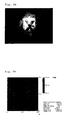
- Figs. 5a and 5b are an optical microscopic image (x 1,000) and an AFM image of the semiconductor nanocrystal pattern. From the Figs. 5a and 5b, it was known that the CdSeS nanocrystals were uniformly dispersed in CdSeS nanocrystal pattern.
- Example 5 Patterning of CdS nanocrystals surface-coordinated with a compound containing a carbon-carbon double bond
- Example 6 Patterning of CdSeS nanocrystals surface-coordinated with a compound containing an acryl group
- Example 7 Patterning of CdS nanocrystals surface-coordinated with a compound containing acryl group
- Example 8 Manufacture of electroluminescent device using nanocrystal pattern
- an organic-inorganic hybrid electroluminescent device was manufactured by employing a thin pattern of the nanocrystals prepared in Preparative Example 1 as a luminescent material.
- PEDOT poly-3,4-ethylenedioxythiophene
- the toluene solution (1wt%) of CdSeS nanocrystals prepared in Preparative Example 1 was spin-coated onto the hole transport layer and dried to form a luminescent layer having a thickness of 5nm.
- the luminescent layer was exposed to 800W UV light having an effective wavelength range of 200-300nm through a mask for 200 seconds and the exposed film was developed with toluene.
- Alq3 tris(8-hydroxyquinolinato) aluminum
- LiF and aluminum were sequentially deposited onto the electron transport layer to thickness of 1nm and 200nm, respectively, to manufacture an organic-inorganic hybrid electroluminescent device.
- An electroluminescent spectrum of the electroluminescent device is shown in Fig. 6.
- the spectrum confirms that light was emitted from the nanocrystals by electrons applied to the device.
- peak emitting wavelength was 520nm, and the FWHM was approximately 40nm.
- intensity of the spectrum was 10 Cd/m 2 and the efficiency of the device was about 0.1%.
Landscapes
- Chemical & Material Sciences (AREA)
- Engineering & Computer Science (AREA)
- Nanotechnology (AREA)
- Crystallography & Structural Chemistry (AREA)
- Physics & Mathematics (AREA)
- Organic Chemistry (AREA)
- General Physics & Mathematics (AREA)
- Metallurgy (AREA)
- Materials Engineering (AREA)
- Optics & Photonics (AREA)
- Life Sciences & Earth Sciences (AREA)
- Composite Materials (AREA)
- Biophysics (AREA)
- Ceramic Engineering (AREA)
- Condensed Matter Physics & Semiconductors (AREA)
- Inorganic Chemistry (AREA)
- Medicinal Chemistry (AREA)
- Chemical Kinetics & Catalysis (AREA)
- Polymers & Plastics (AREA)
- Health & Medical Sciences (AREA)
- Manufacturing & Machinery (AREA)
- Electroluminescent Light Sources (AREA)
- Luminescent Compositions (AREA)
- Materials For Photolithography (AREA)
- Exposure And Positioning Against Photoresist Photosensitive Materials (AREA)
- Inorganic Compounds Of Heavy Metals (AREA)
- Organic Low-Molecular-Weight Compounds And Preparation Thereof (AREA)
Priority Applications (1)
| Application Number | Priority Date | Filing Date | Title |
|---|---|---|---|
| EP17169767.5A EP3240047B1 (fr) | 2003-10-21 | 2004-10-06 | Composition photosensible comprenant des nanocristaux semi-conducteurs et procédé de formation de motif de nanocristal semi-conducteur les utilisant |
Applications Claiming Priority (2)
| Application Number | Priority Date | Filing Date | Title |
|---|---|---|---|
| KR1020030073338A KR100697511B1 (ko) | 2003-10-21 | 2003-10-21 | 광경화성 반도체 나노결정, 반도체 나노결정 패턴형성용 조성물 및 이들을 이용한 반도체 나노결정의 패턴 형성 방법 |
| KR2003073338 | 2003-10-21 |
Related Child Applications (2)
| Application Number | Title | Priority Date | Filing Date |
|---|---|---|---|
| EP17169767.5A Division EP3240047B1 (fr) | 2003-10-21 | 2004-10-06 | Composition photosensible comprenant des nanocristaux semi-conducteurs et procédé de formation de motif de nanocristal semi-conducteur les utilisant |
| EP17169767.5A Division-Into EP3240047B1 (fr) | 2003-10-21 | 2004-10-06 | Composition photosensible comprenant des nanocristaux semi-conducteurs et procédé de formation de motif de nanocristal semi-conducteur les utilisant |
Publications (3)
| Publication Number | Publication Date |
|---|---|
| EP1526584A2 true EP1526584A2 (fr) | 2005-04-27 |
| EP1526584A3 EP1526584A3 (fr) | 2009-09-09 |
| EP1526584B1 EP1526584B1 (fr) | 2017-06-14 |
Family
ID=36944444
Family Applications (2)
| Application Number | Title | Priority Date | Filing Date |
|---|---|---|---|
| EP04256185.2A Expired - Lifetime EP1526584B1 (fr) | 2003-10-21 | 2004-10-06 | Procédé de fabrication d'une couche à motif semiconductrice électroluminescente nanocristallins pour des dispositifs électroluminescents hybrides organiques-inorganiques, et d'un dispositif électroluminescent hybride organique-inorganique utilisant celui-ci. |
| EP17169767.5A Expired - Lifetime EP3240047B1 (fr) | 2003-10-21 | 2004-10-06 | Composition photosensible comprenant des nanocristaux semi-conducteurs et procédé de formation de motif de nanocristal semi-conducteur les utilisant |
Family Applications After (1)
| Application Number | Title | Priority Date | Filing Date |
|---|---|---|---|
| EP17169767.5A Expired - Lifetime EP3240047B1 (fr) | 2003-10-21 | 2004-10-06 | Composition photosensible comprenant des nanocristaux semi-conducteurs et procédé de formation de motif de nanocristal semi-conducteur les utilisant |
Country Status (5)
| Country | Link |
|---|---|
| US (4) | US7199393B2 (fr) |
| EP (2) | EP1526584B1 (fr) |
| JP (2) | JP2005128539A (fr) |
| KR (1) | KR100697511B1 (fr) |
| CN (1) | CN1655057B (fr) |
Cited By (7)
| Publication number | Priority date | Publication date | Assignee | Title |
|---|---|---|---|---|
| US7294449B1 (en) | 2003-12-31 | 2007-11-13 | Kovio, Inc. | Radiation patternable functional materials, methods of their use, and structures formed therefrom |
| EP3136174A1 (fr) * | 2015-08-21 | 2017-03-01 | Samsung Electronics Co., Ltd. | Compositions photosensibles, leurs procédés de préparation, et préparé de composites polymères à points quantiques |
| EP3147708A1 (fr) * | 2015-08-21 | 2017-03-29 | Samsung Electronics Co., Ltd. | Compositions photosensibles, leurs procédés de préparation et composites polymères à points quantiques préparés à partir de ceux-ci |
| EP3255117A4 (fr) * | 2015-07-13 | 2018-07-25 | BOE Technology Group Co., Ltd. | Complexe luminescent, matériau luminescent, substrat d'affichage, procédé de préparation et dispositif d'affichage |
| CN108445714A (zh) * | 2017-02-16 | 2018-08-24 | 住友化学株式会社 | 固化性树脂组合物、固化膜及显示装置 |
| US10983432B2 (en) | 2015-08-24 | 2021-04-20 | Samsung Electronics Co., Ltd. | Photosensitive compositions, preparation methods thereof, quantum dot polymer composite prepared therefrom |
| US11958998B2 (en) | 2016-08-09 | 2024-04-16 | Samsung Electronics Co., Ltd. | Compositions, quantum dot polymer composites prepared therefrom, and devices including the same |
Families Citing this family (102)
| Publication number | Priority date | Publication date | Assignee | Title |
|---|---|---|---|---|
| KR100697511B1 (ko) * | 2003-10-21 | 2007-03-20 | 삼성전자주식회사 | 광경화성 반도체 나노결정, 반도체 나노결정 패턴형성용 조성물 및 이들을 이용한 반도체 나노결정의 패턴 형성 방법 |
| US7803347B2 (en) * | 2005-07-01 | 2010-09-28 | Tohoku Techno Arch Co., Ltd. | Organically modified fine particles |
| US7645397B2 (en) * | 2004-01-15 | 2010-01-12 | Nanosys, Inc. | Nanocrystal doped matrixes |
| KR100632632B1 (ko) | 2004-05-28 | 2006-10-12 | 삼성전자주식회사 | 나노 결정의 다층 박막 제조 방법 및 이를 이용한유·무기 하이브리드 전기 발광 소자 |
| CN102064102B (zh) * | 2004-06-08 | 2013-10-30 | 桑迪士克公司 | 形成单层纳米结构的方法和器件以及包含这种单层的器件 |
| US7968273B2 (en) | 2004-06-08 | 2011-06-28 | Nanosys, Inc. | Methods and devices for forming nanostructure monolayers and devices including such monolayers |
| US7776758B2 (en) * | 2004-06-08 | 2010-08-17 | Nanosys, Inc. | Methods and devices for forming nanostructure monolayers and devices including such monolayers |
| US8563133B2 (en) | 2004-06-08 | 2013-10-22 | Sandisk Corporation | Compositions and methods for modulation of nanostructure energy levels |
| KR100736521B1 (ko) * | 2004-06-09 | 2007-07-06 | 삼성전자주식회사 | 나노 결정 전기발광 소자 및 그의 제조방법 |
| JP4522840B2 (ja) * | 2004-12-22 | 2010-08-11 | 独立行政法人科学技術振興機構 | フォトマスク、露光装置及び露光方法 |
| US9297092B2 (en) | 2005-06-05 | 2016-03-29 | Qd Vision, Inc. | Compositions, optical component, system including an optical component, devices, and other products |
| US8718437B2 (en) | 2006-03-07 | 2014-05-06 | Qd Vision, Inc. | Compositions, optical component, system including an optical component, devices, and other products |
| WO2007103310A2 (fr) | 2006-03-07 | 2007-09-13 | Qd Vision, Inc. | Objet contenant des nanocristaux semi-conducteurs |
| US8845927B2 (en) * | 2006-06-02 | 2014-09-30 | Qd Vision, Inc. | Functionalized nanoparticles and method |
| US8835941B2 (en) * | 2006-02-09 | 2014-09-16 | Qd Vision, Inc. | Displays including semiconductor nanocrystals and methods of making same |
| US8849087B2 (en) * | 2006-03-07 | 2014-09-30 | Qd Vision, Inc. | Compositions, optical component, system including an optical component, devices, and other products |
| US9874674B2 (en) | 2006-03-07 | 2018-01-23 | Samsung Electronics Co., Ltd. | Compositions, optical component, system including an optical component, devices, and other products |
| WO2007143197A2 (fr) * | 2006-06-02 | 2007-12-13 | Qd Vision, Inc. | Dispositifs émetteurs de lumière et affichages à performances ameliorées |
| US9212056B2 (en) | 2006-06-02 | 2015-12-15 | Qd Vision, Inc. | Nanoparticle including multi-functional ligand and method |
| WO2008085210A2 (fr) * | 2006-09-12 | 2008-07-17 | Qd Vision, Inc. | Affichage electroluminescent utilisé pour afficher un motif prédéterminé |
| WO2008063658A2 (fr) | 2006-11-21 | 2008-05-29 | Qd Vision, Inc. | Nanocristaux à semi-conducteurs et compositions et dispositifs contenant ceux-ci |
| WO2008063652A1 (fr) | 2006-11-21 | 2008-05-29 | Qd Vision, Inc. | Nanocristaux à semi-conducteurs émettant une lumière bleue et compositions et dispositifs contenant ceux-ci |
| WO2008063653A1 (fr) | 2006-11-21 | 2008-05-29 | Qd Vision, Inc. | Nanocristaux semi-conducteurs et compositions et dispositifs les comprenant |
| US8836212B2 (en) | 2007-01-11 | 2014-09-16 | Qd Vision, Inc. | Light emissive printed article printed with quantum dot ink |
| KR100853086B1 (ko) * | 2007-04-25 | 2008-08-19 | 삼성전자주식회사 | 나노결정-금속산화물 복합체 및 그의 제조방법 |
| US7989153B2 (en) * | 2007-07-11 | 2011-08-02 | Qd Vision, Inc. | Method and apparatus for selectively patterning free standing quantum DOT (FSQDT) polymer composites |
| WO2009014707A2 (fr) | 2007-07-23 | 2009-01-29 | Qd Vision, Inc. | Substrat d'amélioration de lumière à point quantique et dispositif d'éclairage le comprenant |
| US8128249B2 (en) | 2007-08-28 | 2012-03-06 | Qd Vision, Inc. | Apparatus for selectively backlighting a material |
| KR101381360B1 (ko) * | 2007-09-17 | 2014-04-14 | 삼성전자주식회사 | 나노결정 3차원 가공방법 및 표시장치 |
| JP5407241B2 (ja) * | 2007-09-28 | 2014-02-05 | 大日本印刷株式会社 | エレクトロルミネッセンス素子 |
| CN102047098B (zh) | 2008-04-03 | 2016-05-04 | Qd视光有限公司 | 包括量子点的发光器件 |
| US9525148B2 (en) | 2008-04-03 | 2016-12-20 | Qd Vision, Inc. | Device including quantum dots |
| WO2009151515A1 (fr) | 2008-05-06 | 2009-12-17 | Qd Vision, Inc. | Dispositifs d'éclairage à semi-conducteurs comprenant des nanoparticules semi-conductrices confinées quantiques |
| US9207385B2 (en) | 2008-05-06 | 2015-12-08 | Qd Vision, Inc. | Lighting systems and devices including same |
| WO2009137053A1 (fr) | 2008-05-06 | 2009-11-12 | Qd Vision, Inc. | Composants optiques, systèmes comprenant un composant optique et dispositifs associés |
| US8642991B2 (en) | 2008-11-11 | 2014-02-04 | Samsung Electronics Co., Ltd. | Photosensitive quantum dot, composition comprising the same and method of forming quantum dot-containing pattern using the composition |
| KR101029299B1 (ko) * | 2008-12-30 | 2011-04-18 | 서울대학교산학협력단 | 유기 발광 소자 및 그 제조 방법 |
| WO2010126606A2 (fr) | 2009-05-01 | 2010-11-04 | Nanosys, Inc. | Matrices fonctionnalisées pour la dispersion de nanostructures |
| CN101805606B (zh) * | 2010-02-22 | 2012-12-12 | 中国科学院苏州纳米技术与纳米仿生研究所 | 一种单分散近红外量子点的制备方法 |
| KR101744904B1 (ko) * | 2010-03-22 | 2017-06-21 | 삼성디스플레이 주식회사 | 양자점-블록공중합체 하이브리드 및 이의 제조 방법과 분산 방법, 그리고 양자점 블록공중합체 하이브리드를 포함하는 발광 소자 및 이의 제조 방법 |
| US9112161B2 (en) * | 2011-03-29 | 2015-08-18 | Inha-Industry Partnership Institute | Hybrid layer including oxide layer or organic layer and organic polymer layer and manufacturing method thereof |
| KR101336831B1 (ko) * | 2012-02-01 | 2013-12-04 | 주식회사 엘엠에스 | 양자점를 포함하는 조성물 및 이를 이용한 장치 |
| BR112014018744B1 (pt) * | 2012-02-03 | 2020-12-15 | Lumileds Holding B.V | Processo para a produção de um polímero sólido com as nanopartículas luminescentes incorporadas no polímero, artigo polimérico luminescente, unidade de iluminação e material luminescente |
| US9139770B2 (en) | 2012-06-22 | 2015-09-22 | Nanosys, Inc. | Silicone ligands for stabilizing quantum dot films |
| TWI596188B (zh) | 2012-07-02 | 2017-08-21 | 奈米系統股份有限公司 | 高度發光奈米結構及其製造方法 |
| JP6065665B2 (ja) * | 2013-03-11 | 2017-01-25 | Jsr株式会社 | 感放射線性樹脂組成物、硬化膜、発光表示素子および発光層の形成方法 |
| JP6250785B2 (ja) | 2013-03-14 | 2017-12-20 | ナノシス・インク. | 無溶媒量子ドット交換方法 |
| EP2853578B1 (fr) | 2013-09-26 | 2017-08-30 | Samsung Electronics Co., Ltd | Particules de nanocristal et procédés permettant de les synthétiser |
| US11746290B2 (en) | 2013-09-26 | 2023-09-05 | Samsung Electronics Co., Ltd. | Nanocrystal particles and processes for synthesizing the same |
| KR101525524B1 (ko) * | 2013-09-26 | 2015-06-03 | 삼성전자주식회사 | 나노 결정 입자 및 그의 합성 방법 |
| US12215266B2 (en) | 2013-09-26 | 2025-02-04 | Samsung Electronics Co., Ltd. | Nanocrystal particles and processes for synthesizing the same |
| US9778510B2 (en) * | 2013-10-08 | 2017-10-03 | Samsung Electronics Co., Ltd. | Nanocrystal polymer composites and production methods thereof |
| JP6171927B2 (ja) * | 2013-12-25 | 2017-08-02 | Jsr株式会社 | 感放射線性樹脂組成物、硬化膜、発光素子および発光層の形成方法 |
| KR102195513B1 (ko) * | 2013-12-24 | 2020-12-28 | 제이에스알 가부시끼가이샤 | 경화성 수지 조성물, 경화막, 발광 소자 및 발광층의 형성 방법 |
| JP6171923B2 (ja) * | 2013-12-24 | 2017-08-02 | Jsr株式会社 | 硬化性樹脂組成物、硬化膜、発光素子、波長変換フィルムおよび発光層の形成方法 |
| JP6427876B2 (ja) * | 2013-12-27 | 2018-11-28 | Jsr株式会社 | 感放射線性樹脂組成物、硬化膜、発光素子および発光層の形成方法 |
| US9966508B2 (en) | 2014-03-04 | 2018-05-08 | Nanoco Technologies Ltd. | Methods for fabricating quantum dot polymer films |
| JP6110421B2 (ja) * | 2014-03-28 | 2017-04-05 | トヨタ自動車株式会社 | フォノン散乱材、ナノコンポジット熱電材料及びその製造方法 |
| TWI690585B (zh) * | 2014-08-11 | 2020-04-11 | 德商漢高股份有限及兩合公司 | 電激發光之經交聯奈米晶體薄膜 |
| KR102092165B1 (ko) * | 2014-09-23 | 2020-03-23 | 동우 화인켐 주식회사 | 감광성 수지 조성물 |
| KR101856615B1 (ko) * | 2014-10-14 | 2018-05-10 | 동우 화인켐 주식회사 | 감광성 수지 조성물 |
| US10509319B2 (en) * | 2015-02-27 | 2019-12-17 | Merck Patent Gmbh | Photosensitive composition and color converting film |
| KR102028439B1 (ko) * | 2015-03-19 | 2019-10-04 | 동우 화인켐 주식회사 | 자발광 감광성 수지 조성물, 이를 포함하는 컬러필터 및 화상표시장치 |
| JP6497251B2 (ja) * | 2015-07-17 | 2019-04-10 | Jsr株式会社 | 硬化膜形成用組成物、硬化膜、発光表示素子、硬化膜の形成方法及び分散液 |
| KR102377521B1 (ko) * | 2015-09-11 | 2022-03-22 | 삼성디스플레이 주식회사 | 감광성 수지 조성물 및 이를 이용한 표시 장치 |
| KR102631400B1 (ko) | 2015-10-22 | 2024-01-29 | 삼성전자주식회사 | 감광성 조성물, 이로부터 제조된 양자점-폴리머 복합체 패턴, 및 이를 포함하는 전자 소자 |
| EP3163372B1 (fr) | 2015-10-26 | 2020-04-29 | Samsung Electronics Co., Ltd. | Point quantique ayant une couche externe polymère, compositions photosensibles le comprenant et motif composite polymère à points quantiques ainsi obtenu |
| FR3043838B1 (fr) | 2015-11-17 | 2018-06-08 | Commissariat A L'energie Atomique Et Aux Energies Alternatives | Procede de fabrication d'une couche contenant des boites quantiques |
| KR101970724B1 (ko) | 2016-06-14 | 2019-04-22 | 삼성에스디아이 주식회사 | 감광성 수지 조성물, 감광성 수지막 및 이를 이용한 컬러필터 |
| US10544168B2 (en) * | 2016-06-15 | 2020-01-28 | Alliance For Sustainable Energy, Llc | Ligand-exchangeable nanoparticles and methods of making the same |
| EP3327813B1 (fr) | 2016-11-25 | 2021-06-30 | Samsung Electronics Co., Ltd. | Dispositif électroluminescent et dispositif d'affichage comprenant un point quantum |
| WO2018195143A1 (fr) * | 2017-04-18 | 2018-10-25 | The University Of Chicago | Nanocristaux inorganiques photoactifs à coiffe de ligand inorganique |
| EP3401380B1 (fr) | 2017-05-11 | 2020-12-23 | Samsung Electronics Co., Ltd. | Particules nanocristallines semi-conductrices et dispositifs les comprenant |
| CN109749733B (zh) | 2017-11-03 | 2023-11-24 | 三星电子株式会社 | 量子点组合物、量子点聚合物复合物、以及包括其的层状结构体和电子装置 |
| JP7221676B2 (ja) | 2017-12-18 | 2023-02-14 | 三星電子株式会社 | 積層構造物及びこれを含む電子装置並びに表示装置 |
| CN109991813B (zh) | 2017-12-29 | 2022-06-21 | 财团法人工业技术研究院 | 感光型复合材料及使用其形成复合薄膜的方法 |
| WO2019186846A1 (fr) * | 2018-03-28 | 2019-10-03 | シャープ株式会社 | Élément électroluminescent et dispositif d'affichage |
| WO2019186847A1 (fr) * | 2018-03-28 | 2019-10-03 | シャープ株式会社 | Élément électroluminescent et procédé de fabrication d'élément électroluminescent |
| CN110858632B (zh) | 2018-08-23 | 2024-07-12 | 三星电子株式会社 | 量子点器件和量子点 |
| US10851298B2 (en) | 2018-08-30 | 2020-12-01 | Samsung Electronics Co., Ltd. | Electronic device including quantum dots |
| EP3656833B1 (fr) | 2018-11-23 | 2025-03-19 | Samsung Display Co., Ltd. | Points quantiques, compositions et composites les comprenant et dispositif électronique les comprenant |
| US11740495B2 (en) | 2018-11-29 | 2023-08-29 | Samsung Electronics Co., Ltd. | Quantum dots and devices including the same |
| EP3753996A1 (fr) | 2019-06-18 | 2020-12-23 | Samsung Display Co., Ltd. | Points quantiques, composition ou composite les comprenant et dispositif électronique les comprenant |
| US11499098B2 (en) | 2019-08-29 | 2022-11-15 | Samsung Electronics Co., Ltd. | Quantum dots and device including the same |
| EP3809474B1 (fr) | 2019-10-18 | 2023-07-19 | Samsung Electronics Co., Ltd. | Dispositif électroluminescent à points quantiques et dispositif électronique |
| CN112708414A (zh) | 2019-10-25 | 2021-04-27 | 三星电子株式会社 | 核壳量子点、量子点聚合物复合物及显示装置 |
| EP3819354B1 (fr) | 2019-11-08 | 2023-08-09 | Samsung Electronics Co., Ltd. | Points quinznp/znse/zns antiques et composite et dispositif d'affichage les comprenant |
| CN110989295A (zh) * | 2019-11-18 | 2020-04-10 | 中国科学院上海光学精密机械研究所 | 一种激光热模光刻图像反转胶及其光刻方法 |
| KR102718895B1 (ko) | 2019-12-16 | 2024-10-16 | 삼성전자주식회사 | 발광소자와 그 제조방법 |
| KR102911183B1 (ko) | 2019-12-31 | 2026-01-14 | 삼성디스플레이 주식회사 | 색변환 부재 및 이를 포함하는 표시 장치 |
| KR102820492B1 (ko) | 2020-03-13 | 2025-06-13 | 삼성디스플레이 주식회사 | 양자점 및 이를 포함한 복합체와 표시소자 |
| JP7321972B2 (ja) * | 2020-05-25 | 2023-08-07 | 信越化学工業株式会社 | 量子ドット含有重合体とその製造方法 |
| KR102806843B1 (ko) | 2020-07-01 | 2025-05-12 | 삼성전자주식회사 | 발광 소자 및 이를 포함하는 표시 장치 |
| CN114516962B (zh) * | 2020-11-19 | 2024-04-26 | 北京鼎材科技有限公司 | 一种高透光敏树脂及使用其的彩色光敏树脂组合物 |
| KR20220105715A (ko) | 2021-01-20 | 2022-07-28 | 삼성디스플레이 주식회사 | 광 제어 부재의 제조 방법 및 그 광 제어 부재를 포함하는 표시 장치의 제조 방법 |
| KR20220125630A (ko) | 2021-03-05 | 2022-09-14 | 삼성전자주식회사 | 발광성 나노구조체, 및 이를 포함하는 색변환패널과 전자소자 |
| KR20230001556A (ko) | 2021-06-28 | 2023-01-04 | 삼성전자주식회사 | 표시 장치 및 발광소자 |
| KR102367520B1 (ko) * | 2021-07-15 | 2022-02-24 | 덕산네오룩스 주식회사 | 반도체나노입자-리간드 복합체, 그 제조방법, 감광성 수지 조성물, 광학필름, 전기발광다이오드 및 전자장치 |
| US20240360357A1 (en) * | 2021-12-29 | 2024-10-31 | Beijing Boe Technology Development Co., Ltd. | Quantum dot ligand, preparation method for quantum dot film layer, and quantum dot light emitting device |
| CN117682957A (zh) * | 2022-08-22 | 2024-03-12 | 华为技术有限公司 | 配体化合物、复合物及其应用 |
| JP7830283B2 (ja) * | 2022-10-05 | 2026-03-16 | 信越化学工業株式会社 | 感光性樹脂組成物、感光性樹脂皮膜、感光性ドライフィルム、パターン形成方法、及び発光素子 |
| CN118344871B (zh) * | 2023-09-19 | 2025-10-31 | 苏州星烁纳米科技有限公司 | 具有反应活性的纳米晶、纳米晶光刻液、电致发光纳米晶层及其制备方法、电致发光器件 |
Citations (7)
| Publication number | Priority date | Publication date | Assignee | Title |
|---|---|---|---|---|
| EP0622439A1 (fr) | 1993-04-20 | 1994-11-02 | Koninklijke Philips Electronics N.V. | Particules semiconductrices dopées par un activateur à l'échelle du quantum |
| US5559057A (en) | 1994-03-24 | 1996-09-24 | Starfire Electgronic Development & Marketing Ltd. | Method for depositing and patterning thin films formed by fusing nanocrystalline precursors |
| US5751018A (en) | 1991-11-22 | 1998-05-12 | The Regents Of The University Of California | Semiconductor nanocrystals covalently bound to solid inorganic surfaces using self-assembled monolayers |
| US6139626A (en) | 1998-09-04 | 2000-10-31 | Nec Research Institute, Inc. | Three-dimensionally patterned materials and methods for manufacturing same using nanocrystals |
| US20020110180A1 (en) | 2001-02-09 | 2002-08-15 | Barney Alfred A. | Temperature-sensing composition |
| WO2003050329A2 (fr) | 2001-07-30 | 2003-06-19 | The Board Of Trustees Of The University Of Arkansas | Nanocristaux colloidaux de haute qualite et leurs procedes de preparation dans des solvants disperses |
| US6602671B1 (en) | 1998-09-18 | 2003-08-05 | Massachusetts Institute Of Technology | Semiconductor nanocrystals for inventory control |
Family Cites Families (37)
| Publication number | Priority date | Publication date | Assignee | Title |
|---|---|---|---|---|
| JP2825558B2 (ja) * | 1989-10-25 | 1998-11-18 | 株式会社日立製作所 | 組成物及びこの樹脂組成物を使用した多層プリント回路板の製造方法 |
| US5178959A (en) * | 1991-03-27 | 1993-01-12 | General Electric Company | Epoxy-functional fluorosilicones |
| US5537000A (en) * | 1994-04-29 | 1996-07-16 | The Regents, University Of California | Electroluminescent devices formed using semiconductor nanocrystals as an electron transport media and method of making such electroluminescent devices |
| US5789655A (en) * | 1994-05-13 | 1998-08-04 | The Regents Of The University Of California | Transgenic animals expressing artificial epitope-tagged proteins |
| DE19502541A1 (de) * | 1995-01-27 | 1996-08-08 | Bosch Gmbh Robert | Elektrolumineszierendes System |
| JPH10186426A (ja) * | 1996-10-24 | 1998-07-14 | Mitsui Chem Inc | 光重合性樹脂組成物 |
| US6259506B1 (en) * | 1997-02-18 | 2001-07-10 | Spectra Science Corporation | Field activated security articles including polymer dispersed liquid crystals, and including micro-encapsulated field affected materials |
| JPH1127621A (ja) | 1997-07-02 | 1999-01-29 | Sony Corp | 画像データ記録装置とその方法、および、画像データ記録再生装置 |
| JP3885302B2 (ja) | 1997-07-30 | 2007-02-21 | 日産自動車株式会社 | 筒内直接噴射式火花点火エンジンの排気浄化装置 |
| US6322901B1 (en) * | 1997-11-13 | 2001-11-27 | Massachusetts Institute Of Technology | Highly luminescent color-selective nano-crystalline materials |
| EP1116036B1 (fr) | 1998-09-18 | 2004-08-11 | Massachusetts Institute Of Technology | Nanocristaux semiconducteurs fluorescents hydrosolubles |
| JP4404489B2 (ja) * | 1998-09-18 | 2010-01-27 | マサチューセッツ インスティテュート オブ テクノロジー | 水溶性蛍光半導体ナノ結晶 |
| US6251303B1 (en) * | 1998-09-18 | 2001-06-26 | Massachusetts Institute Of Technology | Water-soluble fluorescent nanocrystals |
| DE59913725D1 (de) | 1998-09-30 | 2006-09-14 | Siemens Ag | Verfahren und Anordnung zur rechnergestützten Ermittlung von Clustern zur Erkennung von Schaumbildung in einer Waschmaschine sowie Verfahren und Anordnung zur Erkennung von Schaumbildung in einer Waschmaschine |
| US6569602B1 (en) * | 1998-10-05 | 2003-05-27 | E. I. Du Pont De Nemours And Company | Ionization radiation imageable photopolymer compositions |
| US6306559B1 (en) * | 1999-01-26 | 2001-10-23 | Mitsubishi Chemical Corporation | Organic electroluminescent device comprising a patterned photosensitive composition and a method for producing same |
| JP2000228233A (ja) * | 1999-02-04 | 2000-08-15 | Fuji Photo Film Co Ltd | 色素吸着半導体微粒子および半導体微粒子への色素吸着方法ならびに光電変換素子および光電気化学電池 |
| JP2000242002A (ja) * | 1999-02-23 | 2000-09-08 | Mitsubishi Chemicals Corp | 電子写真感光体 |
| JP4410894B2 (ja) * | 2000-01-21 | 2010-02-03 | 富士通マイクロエレクトロニクス株式会社 | 半導体装置 |
| US6797412B1 (en) * | 2000-04-11 | 2004-09-28 | University Of Connecticut | Full color display structures using pseudomorphic cladded quantum dot nanophosphor thin films |
| AU2001292783A1 (en) * | 2000-09-19 | 2002-04-02 | Shipley Company, L.L.C. | Antireflective composition |
| US6649138B2 (en) * | 2000-10-13 | 2003-11-18 | Quantum Dot Corporation | Surface-modified semiconductive and metallic nanoparticles having enhanced dispersibility in aqueous media |
| JP2002246642A (ja) * | 2001-02-13 | 2002-08-30 | Canon Inc | 窒化物系化合物半導体発光素子 |
| US7153703B2 (en) | 2001-05-14 | 2006-12-26 | Board Of Trustees Of The University Of Arkansas N. A. | Synthesis of stable colloidal nanocrystals using organic dendrons |
| JP3977038B2 (ja) * | 2001-08-27 | 2007-09-19 | 株式会社半導体エネルギー研究所 | レーザ照射装置およびレーザ照射方法 |
| US20030073042A1 (en) * | 2001-10-17 | 2003-04-17 | Cernigliaro George J. | Process and materials for formation of patterned films of functional materials |
| US20040007169A1 (en) * | 2002-01-28 | 2004-01-15 | Mitsubishi Chemical Corporation | Semiconductor nanoparticles and thin film containing the same |
| JP4100165B2 (ja) * | 2002-01-28 | 2008-06-11 | Jsr株式会社 | 感光性誘電体形成用組成物、誘電体および電子部品 |
| US7700200B2 (en) * | 2002-03-29 | 2010-04-20 | Massachusetts Institute Of Technology | Light emitting device including semiconductor nanocrystals |
| US7534488B2 (en) * | 2003-09-10 | 2009-05-19 | The Regents Of The University Of California | Graded core/shell semiconductor nanorods and nanorod barcodes |
| US7098525B2 (en) * | 2003-05-08 | 2006-08-29 | 3M Innovative Properties Company | Organic polymers, electronic devices, and methods |
| KR100965373B1 (ko) * | 2003-06-10 | 2010-06-22 | 삼성전자주식회사 | 감광성 금속 나노입자 및 이를 이용한 도전성 패턴형성방법 |
| US7879696B2 (en) * | 2003-07-08 | 2011-02-01 | Kovio, Inc. | Compositions and methods for forming a semiconducting and/or silicon-containing film, and structures formed therefrom |
| JP4058720B2 (ja) * | 2003-08-29 | 2008-03-12 | 独立行政法人科学技術振興機構 | コア・シェル構造体からなる光記録媒体及びその調製方法 |
| KR100697511B1 (ko) * | 2003-10-21 | 2007-03-20 | 삼성전자주식회사 | 광경화성 반도체 나노결정, 반도체 나노결정 패턴형성용 조성물 및 이들을 이용한 반도체 나노결정의 패턴 형성 방법 |
| KR100632632B1 (ko) * | 2004-05-28 | 2006-10-12 | 삼성전자주식회사 | 나노 결정의 다층 박막 제조 방법 및 이를 이용한유·무기 하이브리드 전기 발광 소자 |
| KR100736521B1 (ko) * | 2004-06-09 | 2007-07-06 | 삼성전자주식회사 | 나노 결정 전기발광 소자 및 그의 제조방법 |
-
2003
- 2003-10-21 KR KR1020030073338A patent/KR100697511B1/ko not_active Expired - Lifetime
-
2004
- 2004-04-01 US US10/814,264 patent/US7199393B2/en not_active Expired - Lifetime
- 2004-10-06 EP EP04256185.2A patent/EP1526584B1/fr not_active Expired - Lifetime
- 2004-10-06 EP EP17169767.5A patent/EP3240047B1/fr not_active Expired - Lifetime
- 2004-10-20 JP JP2004305592A patent/JP2005128539A/ja active Pending
- 2004-10-21 CN CN200410102383XA patent/CN1655057B/zh not_active Expired - Lifetime
-
2006
- 2006-03-20 US US11/378,482 patent/US7476487B2/en not_active Expired - Lifetime
-
2008
- 2008-07-17 US US12/219,231 patent/US8911883B2/en not_active Expired - Lifetime
-
2010
- 2010-09-21 JP JP2010210908A patent/JP2011046951A/ja not_active Withdrawn
-
2012
- 2012-07-09 US US13/544,761 patent/US8758864B2/en not_active Expired - Lifetime
Patent Citations (7)
| Publication number | Priority date | Publication date | Assignee | Title |
|---|---|---|---|---|
| US5751018A (en) | 1991-11-22 | 1998-05-12 | The Regents Of The University Of California | Semiconductor nanocrystals covalently bound to solid inorganic surfaces using self-assembled monolayers |
| EP0622439A1 (fr) | 1993-04-20 | 1994-11-02 | Koninklijke Philips Electronics N.V. | Particules semiconductrices dopées par un activateur à l'échelle du quantum |
| US5559057A (en) | 1994-03-24 | 1996-09-24 | Starfire Electgronic Development & Marketing Ltd. | Method for depositing and patterning thin films formed by fusing nanocrystalline precursors |
| US6139626A (en) | 1998-09-04 | 2000-10-31 | Nec Research Institute, Inc. | Three-dimensionally patterned materials and methods for manufacturing same using nanocrystals |
| US6602671B1 (en) | 1998-09-18 | 2003-08-05 | Massachusetts Institute Of Technology | Semiconductor nanocrystals for inventory control |
| US20020110180A1 (en) | 2001-02-09 | 2002-08-15 | Barney Alfred A. | Temperature-sensing composition |
| WO2003050329A2 (fr) | 2001-07-30 | 2003-06-19 | The Board Of Trustees Of The University Of Arkansas | Nanocristaux colloidaux de haute qualite et leurs procedes de preparation dans des solvants disperses |
Non-Patent Citations (1)
| Title |
|---|
| BRAVO-VASQUEZ ET AL., POLYMERIC MATERIAL SCIENCE AND ENGINEERING, vol. 81, 1999, pages 16 - 17 |
Cited By (12)
| Publication number | Priority date | Publication date | Assignee | Title |
|---|---|---|---|---|
| US7294449B1 (en) | 2003-12-31 | 2007-11-13 | Kovio, Inc. | Radiation patternable functional materials, methods of their use, and structures formed therefrom |
| EP3255117A4 (fr) * | 2015-07-13 | 2018-07-25 | BOE Technology Group Co., Ltd. | Complexe luminescent, matériau luminescent, substrat d'affichage, procédé de préparation et dispositif d'affichage |
| US10287498B2 (en) | 2015-07-13 | 2019-05-14 | Boe Technology Group Co., Ltd. | Luminescent complex, luminescent material, substrate for display and production method thereof, and display apparatus |
| EP3136174A1 (fr) * | 2015-08-21 | 2017-03-01 | Samsung Electronics Co., Ltd. | Compositions photosensibles, leurs procédés de préparation, et préparé de composites polymères à points quantiques |
| EP3147708A1 (fr) * | 2015-08-21 | 2017-03-29 | Samsung Electronics Co., Ltd. | Compositions photosensibles, leurs procédés de préparation et composites polymères à points quantiques préparés à partir de ceux-ci |
| EP3564750A1 (fr) * | 2015-08-21 | 2019-11-06 | Samsung Electronics Co., Ltd. | Compositions photosensibles, ses procédés de préparation, composite polymère à points quantiques préparé à partir de celles-ci |
| US10983433B2 (en) | 2015-08-21 | 2021-04-20 | Samsung Electronics Co., Ltd. | Photosensitive compositions, preparation methods thereof, and quantum dot polymer composite prepared therefrom |
| US11977329B2 (en) | 2015-08-21 | 2024-05-07 | Samsung Electronics Co., Ltd. | Photosensitive compositions, preparation methods thereof, and quantum dot polymer composite prepared therefrom |
| US10983432B2 (en) | 2015-08-24 | 2021-04-20 | Samsung Electronics Co., Ltd. | Photosensitive compositions, preparation methods thereof, quantum dot polymer composite prepared therefrom |
| US11958998B2 (en) | 2016-08-09 | 2024-04-16 | Samsung Electronics Co., Ltd. | Compositions, quantum dot polymer composites prepared therefrom, and devices including the same |
| CN108445714A (zh) * | 2017-02-16 | 2018-08-24 | 住友化学株式会社 | 固化性树脂组合物、固化膜及显示装置 |
| CN108445714B (zh) * | 2017-02-16 | 2022-12-09 | 住友化学株式会社 | 固化性树脂组合物、固化膜及显示装置 |
Also Published As
| Publication number | Publication date |
|---|---|
| US20050161666A1 (en) | 2005-07-28 |
| EP1526584A3 (fr) | 2009-09-09 |
| CN1655057A (zh) | 2005-08-17 |
| EP3240047B1 (fr) | 2022-07-06 |
| KR20050038120A (ko) | 2005-04-27 |
| JP2005128539A (ja) | 2005-05-19 |
| KR100697511B1 (ko) | 2007-03-20 |
| US7199393B2 (en) | 2007-04-03 |
| JP2011046951A (ja) | 2011-03-10 |
| EP1526584B1 (fr) | 2017-06-14 |
| EP3240047A1 (fr) | 2017-11-01 |
| US20130011635A1 (en) | 2013-01-10 |
| US20080290797A1 (en) | 2008-11-27 |
| US20060199039A1 (en) | 2006-09-07 |
| US7476487B2 (en) | 2009-01-13 |
| CN1655057B (zh) | 2010-12-08 |
| US8758864B2 (en) | 2014-06-24 |
| US8911883B2 (en) | 2014-12-16 |
Similar Documents
| Publication | Publication Date | Title |
|---|---|---|
| EP3240047B1 (fr) | Composition photosensible comprenant des nanocristaux semi-conducteurs et procédé de formation de motif de nanocristal semi-conducteur les utilisant | |
| US10920134B2 (en) | Method for preparing multilayer of nanocrystals, and organic-inorganic hybrid electroluminescence device comprising multilayer of nanocrystals prepared by the method | |
| US6869864B2 (en) | Method for producing quantum dot silicate thin film for light emitting device | |
| KR101588317B1 (ko) | 감광성 양자점, 이를 포함한 조성물 및 상기 조성물을 이용한 양자점-함유 패턴 형성 방법 | |
| CN114839835A (zh) | 量子点的无损光刻图案化方法和设备 | |
| EP3385355B1 (fr) | Procédés de fabrication de films polymères à points quantiques | |
| KR102820492B1 (ko) | 양자점 및 이를 포함한 복합체와 표시소자 | |
| JP2021522397A (ja) | 架橋された配位子 | |
| EP3898886A1 (fr) | Points quantiques à enveloppe mince pour absorption de lumière bleue améliorée | |
| KR101107488B1 (ko) | 나노입자의 분산방법 | |
| Zhang et al. | Suppressed blinking behavior of CdSe/CdS QDs by polymer coating | |
| CN117242157A (zh) | 一种混合物及其在光电领域的应用 | |
| JPH0950057A (ja) | 半導体超微粒子含有ポリマー粒子 | |
| KR20220016464A (ko) | 반도체 나노입자 복합체, 반도체 나노입자 복합체 조성물, 반도체 나노입자 복합체 경화막, 반도체 나노입자 복합체 분산액, 반도체 나노입자 복합체 조성물의 제조 방법 및 반도체 나노입자 복합체 경화막의 제조 방법 | |
| KR20220061042A (ko) | 페로브스카이트 색변환 소재 및 이의 제조방법 | |
| KR100636959B1 (ko) | 나노 결정-고분자 다층 박막의 제조 방법 및 이를 이용한유·무기 하이브리드 전기 발광 소자 | |
| KR102825651B1 (ko) | 반도체 나노입자 복합체 분산액, 반도체 나노입자 복합체, 반도체 나노입자 복합체 조성물 및 반도체 나노입자 복합체 경화막 | |
| Antolini | Direct Optical Patterning of Quantum Dots: One Strategy, Different Chemical Processes. Nanomaterials 2023, 13, 2008 | |
| Sill | Quantum dot-polymer nanocomposites: New materials for dispersion, encapsulation, and electronic applications |
Legal Events
| Date | Code | Title | Description |
|---|---|---|---|
| PUAI | Public reference made under article 153(3) epc to a published international application that has entered the european phase |
Free format text: ORIGINAL CODE: 0009012 |
|
| AK | Designated contracting states |
Kind code of ref document: A2 Designated state(s): AT BE BG CH CY CZ DE DK EE ES FI FR GB GR HU IE IT LI LU MC NL PL PT RO SE SI SK TR |
|
| AX | Request for extension of the european patent |
Extension state: AL HR LT LV MK |
|
| RIN1 | Information on inventor provided before grant (corrected) |
Inventor name: AHN, TAE KYUNG Inventor name: PARK, JONG JIN Inventor name: JANG, EUN JOO Inventor name: LEE, SUNG HUN Inventor name: JUN, SHIN AE |
|
| RIN1 | Information on inventor provided before grant (corrected) |
Inventor name: LEE, SUNG HUN Inventor name: JUN, SHIN AE Inventor name: JANG, EUN JOO Inventor name: PARK, JONG JIN Inventor name: AHN, TAE KYUNG |
|
| PUAL | Search report despatched |
Free format text: ORIGINAL CODE: 0009013 |
|
| AK | Designated contracting states |
Kind code of ref document: A3 Designated state(s): AT BE BG CH CY CZ DE DK EE ES FI FR GB GR HU IE IT LI LU MC NL PL PT RO SE SI SK TR |
|
| AX | Request for extension of the european patent |
Extension state: AL HR LT LV MK |
|
| 17P | Request for examination filed |
Effective date: 20100127 |
|
| AKX | Designation fees paid |
Designated state(s): AT DE FI FR GB NL |
|
| 17Q | First examination report despatched |
Effective date: 20101007 |
|
| RAP1 | Party data changed (applicant data changed or rights of an application transferred) |
Owner name: SAMSUNG ELECTRONICS CO., LTD. |
|
| REG | Reference to a national code |
Ref country code: DE Ref legal event code: R079 Ref document number: 602004051387 Country of ref document: DE Free format text: PREVIOUS MAIN CLASS: H01L0033000000 Ipc: H01L0051540000 |
|
| GRAP | Despatch of communication of intention to grant a patent |
Free format text: ORIGINAL CODE: EPIDOSNIGR1 |
|
| STAA | Information on the status of an ep patent application or granted ep patent |
Free format text: STATUS: GRANT OF PATENT IS INTENDED |
|
| RIC1 | Information provided on ipc code assigned before grant |
Ipc: H01L 51/54 20060101AFI20161201BHEP |
|
| INTG | Intention to grant announced |
Effective date: 20161221 |
|
| GRAS | Grant fee paid |
Free format text: ORIGINAL CODE: EPIDOSNIGR3 |
|
| GRAA | (expected) grant |
Free format text: ORIGINAL CODE: 0009210 |
|
| STAA | Information on the status of an ep patent application or granted ep patent |
Free format text: STATUS: THE PATENT HAS BEEN GRANTED |
|
| AK | Designated contracting states |
Kind code of ref document: B1 Designated state(s): AT DE FI FR GB NL |
|
| REG | Reference to a national code |
Ref country code: GB Ref legal event code: FG4D |
|
| REG | Reference to a national code |
Ref country code: AT Ref legal event code: REF Ref document number: 901727 Country of ref document: AT Kind code of ref document: T Effective date: 20170615 |
|
| REG | Reference to a national code |
Ref country code: DE Ref legal event code: R096 Ref document number: 602004051387 Country of ref document: DE |
|
| REG | Reference to a national code |
Ref country code: FR Ref legal event code: PLFP Year of fee payment: 14 |
|
| REG | Reference to a national code |
Ref country code: NL Ref legal event code: MP Effective date: 20170614 |
|
| PG25 | Lapsed in a contracting state [announced via postgrant information from national office to epo] |
Ref country code: FI Free format text: LAPSE BECAUSE OF FAILURE TO SUBMIT A TRANSLATION OF THE DESCRIPTION OR TO PAY THE FEE WITHIN THE PRESCRIBED TIME-LIMIT Effective date: 20170614 |
|
| REG | Reference to a national code |
Ref country code: AT Ref legal event code: MK05 Ref document number: 901727 Country of ref document: AT Kind code of ref document: T Effective date: 20170614 |
|
| PG25 | Lapsed in a contracting state [announced via postgrant information from national office to epo] |
Ref country code: NL Free format text: LAPSE BECAUSE OF FAILURE TO SUBMIT A TRANSLATION OF THE DESCRIPTION OR TO PAY THE FEE WITHIN THE PRESCRIBED TIME-LIMIT Effective date: 20170614 |
|
| PG25 | Lapsed in a contracting state [announced via postgrant information from national office to epo] |
Ref country code: AT Free format text: LAPSE BECAUSE OF FAILURE TO SUBMIT A TRANSLATION OF THE DESCRIPTION OR TO PAY THE FEE WITHIN THE PRESCRIBED TIME-LIMIT Effective date: 20170614 |
|
| REG | Reference to a national code |
Ref country code: DE Ref legal event code: R097 Ref document number: 602004051387 Country of ref document: DE |
|
| PLBE | No opposition filed within time limit |
Free format text: ORIGINAL CODE: 0009261 |
|
| STAA | Information on the status of an ep patent application or granted ep patent |
Free format text: STATUS: NO OPPOSITION FILED WITHIN TIME LIMIT |
|
| 26N | No opposition filed |
Effective date: 20180315 |
|
| REG | Reference to a national code |
Ref country code: FR Ref legal event code: PLFP Year of fee payment: 15 |
|
| REG | Reference to a national code |
Ref country code: DE Ref legal event code: R079 Ref document number: 602004051387 Country of ref document: DE Free format text: PREVIOUS MAIN CLASS: H01L0051540000 Ipc: H10K0085000000 |
|
| P01 | Opt-out of the competence of the unified patent court (upc) registered |
Effective date: 20230519 |
|
| PGFP | Annual fee paid to national office [announced via postgrant information from national office to epo] |
Ref country code: GB Payment date: 20230920 Year of fee payment: 20 |
|
| PGFP | Annual fee paid to national office [announced via postgrant information from national office to epo] |
Ref country code: FR Payment date: 20230922 Year of fee payment: 20 |
|
| PGFP | Annual fee paid to national office [announced via postgrant information from national office to epo] |
Ref country code: DE Payment date: 20230920 Year of fee payment: 20 |
|
| REG | Reference to a national code |
Ref country code: DE Ref legal event code: R071 Ref document number: 602004051387 Country of ref document: DE |
|
| REG | Reference to a national code |
Ref country code: GB Ref legal event code: PE20 Expiry date: 20241005 |
|
| PG25 | Lapsed in a contracting state [announced via postgrant information from national office to epo] |
Ref country code: GB Free format text: LAPSE BECAUSE OF EXPIRATION OF PROTECTION Effective date: 20241005 |
|
| PG25 | Lapsed in a contracting state [announced via postgrant information from national office to epo] |
Ref country code: GB Free format text: LAPSE BECAUSE OF EXPIRATION OF PROTECTION Effective date: 20241005 |