EP1530205A2 - Capteur optique mince - Google Patents
Capteur optique mince Download PDFInfo
- Publication number
- EP1530205A2 EP1530205A2 EP04020327A EP04020327A EP1530205A2 EP 1530205 A2 EP1530205 A2 EP 1530205A2 EP 04020327 A EP04020327 A EP 04020327A EP 04020327 A EP04020327 A EP 04020327A EP 1530205 A2 EP1530205 A2 EP 1530205A2
- Authority
- EP
- European Patent Office
- Prior art keywords
- optical pickup
- bonding pads
- substrate
- leaf spring
- slim
- Prior art date
- Legal status (The legal status is an assumption and is not a legal conclusion. Google has not performed a legal analysis and makes no representation as to the accuracy of the status listed.)
- Granted
Links
Images


Classifications
-
- G—PHYSICS
- G11—INFORMATION STORAGE
- G11B—INFORMATION STORAGE BASED ON RELATIVE MOVEMENT BETWEEN RECORD CARRIER AND TRANSDUCER
- G11B7/00—Recording or reproducing by optical means, e.g. recording using a thermal beam of optical radiation by modifying optical properties or the physical structure, reproducing using an optical beam at lower power by sensing optical properties; Record carriers therefor
- G11B7/08—Disposition or mounting of heads or light sources relatively to record carriers
-
- G—PHYSICS
- G11—INFORMATION STORAGE
- G11B—INFORMATION STORAGE BASED ON RELATIVE MOVEMENT BETWEEN RECORD CARRIER AND TRANSDUCER
- G11B7/00—Recording or reproducing by optical means, e.g. recording using a thermal beam of optical radiation by modifying optical properties or the physical structure, reproducing using an optical beam at lower power by sensing optical properties; Record carriers therefor
- G11B7/12—Heads, e.g. forming of the optical beam spot or modulation of the optical beam
- G11B7/125—Optical beam sources therefor, e.g. laser control circuitry specially adapted for optical storage devices; Modulators, e.g. means for controlling the size or intensity of optical spots or optical traces
- G11B7/126—Circuits, methods or arrangements for laser control or stabilisation
- G11B7/1263—Power control during transducing, e.g. by monitoring
-
- G—PHYSICS
- G11—INFORMATION STORAGE
- G11B—INFORMATION STORAGE BASED ON RELATIVE MOVEMENT BETWEEN RECORD CARRIER AND TRANSDUCER
- G11B7/00—Recording or reproducing by optical means, e.g. recording using a thermal beam of optical radiation by modifying optical properties or the physical structure, reproducing using an optical beam at lower power by sensing optical properties; Record carriers therefor
- G11B7/08—Disposition or mounting of heads or light sources relatively to record carriers
- G11B7/085—Disposition or mounting of heads or light sources relatively to record carriers with provision for moving the light beam into, or out of, its operative position or across tracks, otherwise than during the transducing operation, e.g. for adjustment or preliminary positioning or track change or selection
- G11B7/0857—Arrangements for mechanically moving the whole head
- G11B7/08576—Swinging-arm positioners
-
- G—PHYSICS
- G11—INFORMATION STORAGE
- G11B—INFORMATION STORAGE BASED ON RELATIVE MOVEMENT BETWEEN RECORD CARRIER AND TRANSDUCER
- G11B7/00—Recording or reproducing by optical means, e.g. recording using a thermal beam of optical radiation by modifying optical properties or the physical structure, reproducing using an optical beam at lower power by sensing optical properties; Record carriers therefor
- G11B7/12—Heads, e.g. forming of the optical beam spot or modulation of the optical beam
- G11B7/123—Integrated head arrangements, e.g. with source and detectors mounted on the same substrate
-
- G—PHYSICS
- G11—INFORMATION STORAGE
- G11B—INFORMATION STORAGE BASED ON RELATIVE MOVEMENT BETWEEN RECORD CARRIER AND TRANSDUCER
- G11B7/00—Recording or reproducing by optical means, e.g. recording using a thermal beam of optical radiation by modifying optical properties or the physical structure, reproducing using an optical beam at lower power by sensing optical properties; Record carriers therefor
- G11B7/12—Heads, e.g. forming of the optical beam spot or modulation of the optical beam
- G11B7/125—Optical beam sources therefor, e.g. laser control circuitry specially adapted for optical storage devices; Modulators, e.g. means for controlling the size or intensity of optical spots or optical traces
- G11B7/127—Lasers; Multiple laser arrays
-
- G—PHYSICS
- G11—INFORMATION STORAGE
- G11B—INFORMATION STORAGE BASED ON RELATIVE MOVEMENT BETWEEN RECORD CARRIER AND TRANSDUCER
- G11B7/00—Recording or reproducing by optical means, e.g. recording using a thermal beam of optical radiation by modifying optical properties or the physical structure, reproducing using an optical beam at lower power by sensing optical properties; Record carriers therefor
- G11B7/12—Heads, e.g. forming of the optical beam spot or modulation of the optical beam
- G11B7/13—Optical detectors therefor
- G11B7/131—Arrangement of detectors in a multiple array
-
- G—PHYSICS
- G11—INFORMATION STORAGE
- G11B—INFORMATION STORAGE BASED ON RELATIVE MOVEMENT BETWEEN RECORD CARRIER AND TRANSDUCER
- G11B7/00—Recording or reproducing by optical means, e.g. recording using a thermal beam of optical radiation by modifying optical properties or the physical structure, reproducing using an optical beam at lower power by sensing optical properties; Record carriers therefor
- G11B7/12—Heads, e.g. forming of the optical beam spot or modulation of the optical beam
- G11B7/22—Apparatus or processes for the manufacture of optical heads, e.g. assembly
Definitions
- the present invention relates to a slim optical pickup, and more particularly, to a slim optical pickup in which a leaf spring is combined with an upper surface of a semiconductor substrate.
- the semiconductor substrate is a silicon optical bench (SiOB) monolithically manufactured with a photodetector.
- FIG. 1 is a perspective view illustrating a combined SiOB and leaf spring, in which a light source and optical devices are integrated, for use in a conventional slim optical pickup.
- FIG. 2 is a cross-sectional view illustrating a conventional slim optical pickup to which the silicon optical bench and the leaf spring of FIG. 1 are applied.
- a slim optical pickup 10 comprises a silicon optical bench (SiOB) 30 in which a light source 12, such as a laser diode, a monitoring photodetector 34, a sloped mirror 14, and a photodetector 38 are included; a polarized light beam splitter 16; a prism 19 which includes first and second reflection surfaces 13 and 18; spacers 15 and 17 disposed between main substrate 32 and beam splitting 16/prism 19; a hologram optical element (HOE) 20; an objective lens 26 attached to a backside of a predetermined part of a SiOB 30 to face the HOE 20; aperture 24 in main substrate 32; a leaf spring 40 attached to a backside of the SiOB 30; and a heat sink 50 disposed on a surface of the leaf spring 40.
- Wiring 36 electrically connects photodetector 38 to a bonding pad 33.
- 11 corresponds to monitoring mirror 111 described below.
- FIG. 3 is a cross-sectional view illustrating a method of electrically connecting a semiconductor substrate to a leaf spring when assembling a conventional slim optical pickup.
- the conventional slim optical pickup 10 has a structure of combining the leaf spring 40 on the back surface of the SiOB 30.
- this conventional structure when wire bonding wire 62 from a bonding pad 33 of the SiOB 30 to a bonding pad 44 formed on the leaf spring 40, a gap between a side surface of the SiOB 30 and the bonding pad 44 of the leaf spring 40 must be maintained to at least 0.5 mm due to a thickness of a capillary of a wire bonder 60.
- the present invention provides a slim optical pickup that can dissipate heat efficiently.
- the present invention also provides a slim optical pickup having a reduced size.
- the present invention also provides a slim optical pickup having a structure in which a SiOB can be assembled to a leaf spring using a ball grid array (BGA) method.
- BGA ball grid array
- a slim optical pickup comprising a substrate including a light source for generating light, an optical element for irradiating light to an optical disc, a photodetector for receiving light beams reflected by the optical disc, and a plurality of first bonding pads; a heat sink attached to a surface of the substrate; and a supporting means having a plurality of second bonding pads formed on an inner side of an array of the plurality of the first bonding pads on the substrate, facing the heat sink interposing the substrate.
- an optical pickup for recording and reproducing information to and from an optical disc, comprising a substrate including a light source for generating light, an optical element for irradiating light to the optical disc, a photodetector for receiving light beams reflected by the optical disc, and a plurality of bonding pads; a heat sink attached to a surface of the substrate; and a supporting means having a plurality of second bonding pads formed to match an array of the plurality of the first bonding pads on the substrate.
- FIG. 1 is a perspective view illustrating a combined SiOB and leaf spring, in which a light source and optical devices are integrated, for use in a conventional slim optical pickup;
- FIG. 2 is a cross-sectional view illustrating a conventional slim optical pickup to which the SiOB and the leaf spring of FIG. 1 are applied;
- FIG. 3 is a cross-sectional view illustrating a method of electrically connecting a semiconductor substrate to the leaf spring when assembling a conventional slim optical pickup
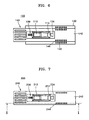
- FIG. 4 is a perspective view of a combined SiOB and a leaf spring, in which a light source and optical devices are integrated, for use in a slim optical pickup according to an embodiment of the present invention
- FIG. 5 is a cross-sectional view of a slim optical pickup according to an embodiment of the present invention employing the SiOB and the leaf spring of FIG. 4;
- FIG. 6 is a plan view of bonding pads and electrical wiring for wire bonding for electrically connecting a SiOB and a leaf spring according to an embodiment of the present invention
- FIG. 7 is a plan view of bonding pads and electrical wiring for assembling a silicon optical bench and a leaf spring using a BGA method according to an embodiment of the present invention.
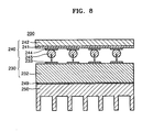
- FIG. 8 is a cross-sectional view for describing bonding pads and ball grids for assembling using the BGA method in FIG 7.
- FIG. 4 is a perspective view of a combined silicon optical bench, in which a light source and optical devices are integrated to a leaf spring for use in a slim optical pickup according to an embodiment of the present invention.
- FIG. 4 shows a slim optical pickup 100 in which a SiOB 130 (including a light source 112, an eight-partitioned photodetector 138, a slope mirror 114, and a monitoring photodetector 134) and a leaf spring 140 (combined to a front surface of the SiOB 130) are electrically connected.
- a SiOB 130 including a light source 112, an eight-partitioned photodetector 138, a slope mirror 114, and a monitoring photodetector 1314
- a leaf spring 140 combined to a front surface of the SiOB 130
- an adhesive 139 is applied on a predetermined surface of the leaf spring 140 except the plurality of bonding pads 144. Further, the adhesive is hardened after assembling the leaf spring 140 and the SiOB 130 by wire bonding.
- FIG. 5 is a cross-sectional view of a slim optical pickup, according to an embodiment of the present invention, to which the silicon optical bench and the leaf spring of FIG. 4 are applied.
- the slim optical pickup 100 comprises the SiOB 130, the leaf spring 140, a heat sink 150, a HOE 120, an objective lens 126, and a prism 119.
- the silicon optical bench 130 includes a light source 112, the eight-partitioned photodetector 138, the slope mirror 114, the monitoring photodetector 134, and a plurality of bonding pads 133.
- the leaf spring 140 includes a leaf spring main body 142 and the bonding pads 144 formed on the leaf spring main body 142. Adhesive 149 bonds silicon optical bench 130 to the heat sink 150.
- a plurality of conductive patterns are formed on the leaf spring 140 and electrically connected to an actuator externally connected to the leaf spring 140 and to other components that constitute the optical pickup assembly.
- the SiOB 130 is formed of silicon, and a groove is formed on the SiOB 130.
- a light source 112 is flip-chip bonded on a bottom surface of the groove.
- Mirrors 114 having a 45° slope are disposed on left and right side surfaces of the groove.
- the bottom surface for mounting the light source 112 and the sloped mirror 114 are formed by dry etching and wet etching the main substrate 132 which is formed of a silicon (Si) wafer having a crystal face of ⁇ 100 ⁇ plane tilted at approximately 9.74°.
- the silicon forming the sloped mirror 114 has a crystal face of ⁇ 111 ⁇ plane.
- the eight-partitioned photodetector 138 and the monitoring photodetector 134 are disposed on the main substrate 132 of the SiOB 130.
- the leaf spring main body 142 of the leaf spring 140 is preferably formed of stainless steel such as SUS304CSPH. Also, the leaf spring 140 and the motor are used for controlling a head of the slim optical pickup 100.
- An aspect of the present invention is that the leaf spring 140 is disposed on an upper surface of the SiOB 130, that is, the same surface on which the photodetectors 134 and 138 are disposed.
- the bonding pads 144 are formed on an upper surface of the leaf spring main body 142.
- the bonding pads 144 are electrically connected to the bonding pads 133 formed on the SiOB 130 by wire bonding. Such connected wirings are electrically connected to external devices along wirings (not shown) formed on the leaf spring 140.
- the leaf spring 140 has an opening through which the eight-partitioned photodetector 138 can receive light beams generated from the light source 112 and reflected by the optical disc.
- a beam generated from a light source 112 enters into a polarized beam splitter 116 of a prism element 119 after being totally reflected by the mirror 114 in an orthogonal direction to the substrate main body 132.
- the polarized beam splitter 116 reflects a light beam polarized in a first direction (hereafter, "first polarized light beam”), but transmits a light beam polarized in a second direction (hereafter, "second polarized light beam”).
- first polarized light beam a light beam polarized in a first direction
- second polarized light beam a light beam polarized in a second direction
- monitoring mirror 111 that portion of the light beam having a large radiation angle such that it falls outside of the area of slope mirror 114 is reflected by monitoring mirror 111 disposed in front of the monitoring photodetector 134.
- the light reflected by the monitoring mirror 111 enters the monitoring photodetector 134.
- the light received by the monitoring photodetector 134 is used for monitoring the amount of light generated from the light source 112.
- the first polarized light beam which has entered into HOE 120 enters into an objective lens 126 after passing through HOE 120.
- a ⁇ /4 plate (quarter wave plate; QWP) (not shown) is further disposed on a light path between the polarized beam splitter 116 and an optical disc D.
- the ⁇ /4 plate delays a phase of either vertically polarized or horizontally polarized incident light by as much as ⁇ /4, and additionally delays a phase of a first polarized light beam passing through the objective lens 126 after being reflected by the optical disc D by as much as ⁇ /4, thereby delaying a phase of the first polarized light beam by as much as ⁇ /2. That is, after passing through the ⁇ /4 plate twice, the first polarized light beam is rotated 90° with respect to the other polarized light beam (here ⁇ is a wavelength of incident light).
- the objective lens 126 focuses the incident light beam on the optical disc D.
- the focused light beam is reflected by the optical disc D and re-enters HOE 120 after passing through the objective lens 126.
- the HOE 120 generates an aberration in the light beam reflected by the optical disc D. Accordingly, the eight-partitioned photodetector 138 can detect a focusing error, a tracking error, or an optical information signal recorded on a recording surface of the optical disc D. That is, the light beam reflected by the optical disc D is divided into 0 th order or ⁇ 1th order by the HOE 120, and the divided light beams are reflected by the first reflection face 113.
- the light beam reflected by the first reflection face 113 enters the polarized beam splitter 116 passing through the ⁇ /4 plate again.
- the phase of the light beam that has passed through the ⁇ /4 plate twice is delayed by as much as ⁇ /2, and then the light beam is transformed to the second polarized light beam orthogonal to the first polarized light beam.
- the second polarized light beam is incident to a second reflection face 118 after passing through the polarized beam splitter 116.
- the second reflection face 118 reflects the incident light beam to the eight-partitioned photodetector 138.
- the eight-partitioned photodetector 138 converts the light signal that has been received into an electrical signal.
- a focusing error, a tracking error, or a tilt error of the optical disc D can be detected using the electrical signal, so that recording and the servo can be controlled. Therefore, the operations of reproducing information stored on the optical disc D can be performed.
- the first and second reflection surfaces 113 and 118 and polarized beam splitter 116 are called a polarizing device.
- Spacer 117 having monitoring mirror 111 is disposed between substrate 132 and the polarizing device.
- Spacer 115 is also disposed between substrate 132 and the polarizing device.
- the eight-partitioned photodetector 138 is employed for controlling the servo and recording and reproducing information stored on the optical disc D by detecting a focusing error, a tracking error, and a tilt error of the optical disc D.
- a variety of different arrangements of photodetectors can be used for the same or similar purpose.
- the present embodiment has been described with reference to a structure where the monitoring photodetector 134 is disposed in front of the monitoring mirror 111.
- the structure can be modified to one in which a semi-transparent mirror is used as the sloped mirror 114 and the photodetector can be embedded on a back side of the sloped mirror 114.
- FIG 6 is a plan view of bonding pads and electrical wiring for wire bonding for electrically connecting a SiOB and a leaf spring according to an embodiment of the present invention.
- the bonding pads 144 formed on the leaf spring 140 can be located at an inner side of an array of the bonding pads 133 formed on the substrate main body 132.
- a width of the leaf spring 140 in the present embodiment is significantly reduced compared to a width of a conventional leaf spring for wire bonding.
- FIG. 7 is a plan view of bonding pads and electrical wiring for the assembly of a SiOB and a leaf spring using a BGA method according to an embodiment of the present invention.
- a leaf spring 240 by forming a leaf spring 240 on an opposite side of a substrate main body 232 of a SiOB 230 on which a heat sink 250 is disposed via adhesive 249, a plurality of bonding pads 244 formed on the leaf spring 240 can be located at a corresponding location to an array of bonding pads 233 formed on the substrate main body 232.
- This configuration allows for the assembly of the SiOB 230 and the leaf spring 240 using a BGA method, which cannot be used in a conventional slim optical pickup structure.
- the slim optical pickup 200 is structured such that the leaf spring 240 is attached to a back side of the SiOB 230, it is technically difficult to form bonding pads by making through holes from a front surface to a back surface of the SiOB 230 for connecting the laser diode as the light source, the eight-partitioned photodetector 238, and the monitoring detector 234 formed on the front surface of the SiOB 230 to external electric signals.
- the SiOB 230 to electrically connect the SiOB 230 to the leaf spring 240 using the BGA method, it is desirable to form the bonding pads 233 on the front surface of the SiOB 230 on which the laser diode and the photodetector are formed.
- the leaf spring 240 includes an opening through which the eight-partitioned photodetector 238 receives a light beam generated from a light source 212 and is reflected by an optical disc D.
- 214 corresponds to slope mirror 114.
- FIG. 8 is a cross-sectional view illustrating bonding pads and ball grids for assembly using the BGA method in FIG. 7.
- the second embodiment of the present invention is identical to the first embodiment of the present invention in function and operation except for the leaf spring.
- the leaf spring 240 is structured as follows.
- the bonding pads 244 having the same shape and arrangement corresponding to those of the bonding pads 233 formed on the main substrate 232 of the SiOB 230 are formed on the insulating film 241. Afterward, a plurality of solder balls 245 are formed on the bonding pads 244 which in turn are formed on the leaf spring 240. Next, the leaf spring 240 is mounted on the SiOB 230 so that the solder balls 245 can be aligned to the bonding pads 233 formed on the main substrate 232 of the SiOB 230.
- the adhesive is applied to a predetermined portion of a contacting surface between the leaf spring 240 and the SiOB 230 except the bonding pads 233 and 244. Then, the adhesive is hardened after assembling the leaf spring 240 and the SiOB 230.
- the leaf spring 240 and the SiOB 230 are electrically connected by melting the solder balls 245 formed on the plurality of the bonding pads 244 of the leaf spring 240.
- the space that previously had to be reserved for extending the width of the leaf spring for conventional wire bonding can be reduced. This is because the space can be formed within an array of the bonding pads of the SiOB.
- the location of a plurality of bonding pads formed on the leaf spring can be aligned corresponding to the plurality of bonding pads formed on the main body of the SiOB.
- the main body of the SiOB can be in direct contact with the heat sink without the leaf spring interposed therebetween, heat generated at the light source can be effectively transmitted to the heat sink.
- the SiOB can be in direct contact with the heat sink, a characteristic of a laser diode that constitutes the light source can be maintained at a optimum condition. Also, since the heat generated at the heat source is not transmitted to the leaf spring, malfunctions of the leaf spring due to thermal expansion of the spring can be prevented.
Landscapes
- Physics & Mathematics (AREA)
- Optics & Photonics (AREA)
- Optical Head (AREA)
Applications Claiming Priority (2)
| Application Number | Priority Date | Filing Date | Title |
|---|---|---|---|
| KR10-2003-0077790A KR100513734B1 (ko) | 2003-11-04 | 2003-11-04 | 박형 광픽업 |
| KR2003077790 | 2003-11-04 |
Publications (3)
| Publication Number | Publication Date |
|---|---|
| EP1530205A2 true EP1530205A2 (fr) | 2005-05-11 |
| EP1530205A3 EP1530205A3 (fr) | 2006-05-24 |
| EP1530205B1 EP1530205B1 (fr) | 2007-12-12 |
Family
ID=34431720
Family Applications (1)
| Application Number | Title | Priority Date | Filing Date |
|---|---|---|---|
| EP04020327A Expired - Lifetime EP1530205B1 (fr) | 2003-11-04 | 2004-08-26 | Capteur optique mince |
Country Status (5)
| Country | Link |
|---|---|
| US (1) | US7471595B2 (fr) |
| EP (1) | EP1530205B1 (fr) |
| JP (1) | JP2005141891A (fr) |
| KR (1) | KR100513734B1 (fr) |
| DE (1) | DE602004010603D1 (fr) |
Cited By (1)
| Publication number | Priority date | Publication date | Assignee | Title |
|---|---|---|---|---|
| WO2009039847A1 (fr) * | 2007-09-28 | 2009-04-02 | Osram Opto Semiconductors Gmbh | Dispositif optoélectronique |
Families Citing this family (6)
| Publication number | Priority date | Publication date | Assignee | Title |
|---|---|---|---|---|
| KR100612838B1 (ko) * | 2004-02-07 | 2006-08-18 | 삼성전자주식회사 | 광학벤치, 이를 사용한 박형광픽업 및 그 제조방법 |
| US7829833B2 (en) * | 2005-05-24 | 2010-11-09 | Olympus Imaging Corp. | Arranging and/or supporting an image pickup device in an image pickup apparatus |
| EP1886309B1 (fr) * | 2005-05-30 | 2009-01-21 | Thomson Licensing | Capteur compact pour microlecteur optique |
| KR101286642B1 (ko) * | 2012-02-07 | 2013-07-22 | 도시바삼성스토리지테크놀러지코리아 주식회사 | 광검출기 유닛 및 이를 구비한 광픽업 및 광정보저장매체 시스템 |
| WO2018125576A1 (fr) | 2016-12-30 | 2018-07-05 | Vuzix Corporation | Guide de lumière avec séparateur de faisceau pour images doubles |
| WO2018125577A1 (fr) * | 2016-12-30 | 2018-07-05 | Vuzix Corporation | Guide de lumière avec séparateur de polarisation pour images doubles |
Family Cites Families (30)
| Publication number | Priority date | Publication date | Assignee | Title |
|---|---|---|---|---|
| US4482986A (en) * | 1981-01-30 | 1984-11-13 | Sony Corporation | Objective lens mount for optical disc player |
| JP2851863B2 (ja) * | 1989-03-14 | 1999-01-27 | ソニー株式会社 | 光ディスクドライバ及び光ピックアップ |
| JPH04139628A (ja) * | 1990-09-28 | 1992-05-13 | Matsushita Electron Corp | 光半導体装置およびその製造方法 |
| JP3021203B2 (ja) * | 1992-08-26 | 2000-03-15 | シャープ株式会社 | 光ピックアップ装置 |
| JP3607741B2 (ja) * | 1994-12-07 | 2005-01-05 | オリンパス株式会社 | 光学ヘッド装置 |
| JPH08221782A (ja) * | 1995-02-15 | 1996-08-30 | Toshiba Corp | 光ヘッド装置の放熱機構 |
| US6163509A (en) * | 1996-07-11 | 2000-12-19 | Toyota Jidosha Kabushiki Kaisha | Magneto-optical recording medium and magneto-optical recorder using the medium |
| DE19748324C2 (de) * | 1997-10-31 | 1999-08-26 | Siemens Ag | Optoelektronisches Sensormodul |
| JP2000004067A (ja) * | 1998-04-16 | 2000-01-07 | Sanyo Electric Co Ltd | 光半導体装置およびこれを実装した光半導体モジュール |
| US6529454B1 (en) * | 1998-07-09 | 2003-03-04 | Sony Corporation | Integrated optical component, optical pickup, and optical disc device |
| JP2000123391A (ja) * | 1998-10-16 | 2000-04-28 | Sharp Corp | 光導波路ユニット、およびこれを用いた光学ヘッド |
| US6416865B1 (en) * | 1998-10-30 | 2002-07-09 | Sumitomo Electric Industries, Ltd. | Hard carbon film and surface acoustic-wave substrate |
| JP2000285422A (ja) * | 1999-03-31 | 2000-10-13 | Hitachi Metals Ltd | ヘッドジンバルアッセンブリーおよびその製造方法 |
| US6970401B2 (en) * | 1999-06-23 | 2005-11-29 | Dphi Acquisitions, Inc. | Fringing field focus motor and mechanism for optical disk drive |
| US7079472B2 (en) * | 1999-06-23 | 2006-07-18 | Dphi Acquisitions, Inc. | Beamshaper for optical head |
| JP2001014720A (ja) * | 1999-06-29 | 2001-01-19 | Toshiba Corp | 光ピックアップ装置 |
| US6831882B1 (en) * | 1999-10-29 | 2004-12-14 | Matsushita Electric Industrial Co., Ltd. | Optical head and optical head feeder |
| CN100392736C (zh) * | 1999-12-07 | 2008-06-04 | 数据播放公司 | 小型光头 |
| JP3766585B2 (ja) * | 2000-09-04 | 2006-04-12 | アルプス電気株式会社 | 磁気ヘッド装置の製造方法 |
| JP4085812B2 (ja) * | 2000-09-06 | 2008-05-14 | 株式会社日立製作所 | 光ヘッドおよび光ディスク装置 |
| US6717893B1 (en) * | 2000-10-04 | 2004-04-06 | Dphi Acquisitions, Inc. | Laser thermal management system |
| JP2003141765A (ja) * | 2001-10-31 | 2003-05-16 | Sony Corp | 光ピックアップ装置および光ピックアップ装置の組み立て方法 |
| JP3743359B2 (ja) | 2001-11-30 | 2006-02-08 | 松下電器産業株式会社 | 光ピックアップ装置 |
| JP2003248950A (ja) * | 2002-02-26 | 2003-09-05 | Ricoh Co Ltd | 光ピックアップ及び記録媒体駆動装置 |
| US6751370B2 (en) * | 2002-03-18 | 2004-06-15 | Umachines, Inc. | Method of aligning a driving force with respect to a movable element using mechanical resonance |
| TWI320568B (en) * | 2002-03-20 | 2010-02-11 | Panasonic Corp | Control method for focus and tracking in pickup apparatus |
| JP4096746B2 (ja) * | 2002-03-20 | 2008-06-04 | 松下電器産業株式会社 | 光ピックアップ装置のフォーカス及びトラッキング制御方法 |
| JP2003338072A (ja) * | 2002-05-16 | 2003-11-28 | Matsushita Electric Ind Co Ltd | 光ヘッド、光ピックアップ装置、及びこれらを用いた光ディスク装置 |
| KR100492534B1 (ko) * | 2002-11-29 | 2005-06-02 | 엘지전자 주식회사 | 광 발생기 모듈, 광 검출기 모듈, 그들을 결합한 광픽업장치 및 그들의 제조방법 |
| KR20040079555A (ko) * | 2003-03-07 | 2004-09-16 | 삼성전자주식회사 | 광헤드 및 그 광헤드의 광경로 조정방법 |
-
2003
- 2003-11-04 KR KR10-2003-0077790A patent/KR100513734B1/ko not_active Expired - Fee Related
-
2004
- 2004-08-26 EP EP04020327A patent/EP1530205B1/fr not_active Expired - Lifetime
- 2004-08-26 JP JP2004246253A patent/JP2005141891A/ja active Pending
- 2004-08-26 DE DE602004010603T patent/DE602004010603D1/de not_active Expired - Lifetime
- 2004-10-12 US US10/960,924 patent/US7471595B2/en not_active Expired - Fee Related
Cited By (1)
| Publication number | Priority date | Publication date | Assignee | Title |
|---|---|---|---|---|
| WO2009039847A1 (fr) * | 2007-09-28 | 2009-04-02 | Osram Opto Semiconductors Gmbh | Dispositif optoélectronique |
Also Published As
| Publication number | Publication date |
|---|---|
| JP2005141891A (ja) | 2005-06-02 |
| EP1530205A3 (fr) | 2006-05-24 |
| EP1530205B1 (fr) | 2007-12-12 |
| DE602004010603D1 (de) | 2008-01-24 |
| US20050094534A1 (en) | 2005-05-05 |
| KR100513734B1 (ko) | 2005-09-08 |
| KR20050042714A (ko) | 2005-05-10 |
| US7471595B2 (en) | 2008-12-30 |
Similar Documents
| Publication | Publication Date | Title |
|---|---|---|
| US6853042B2 (en) | Hybrid optical element and photodetector device | |
| US7471595B2 (en) | Slim optical pickup | |
| JP2004207639A (ja) | 半導体集積装置 | |
| US7095682B2 (en) | Compact optical signal detecting mechanism and optical storage device having improved signal quality | |
| JP2001056952A (ja) | 光ヘッド装置およびその製造方法 | |
| US20070264744A1 (en) | Optical bench, slim optical pickup employing the same and method of manufacturing the optical bench | |
| CN100391064C (zh) | 半导体激光装置 | |
| KR20000069725A (ko) | 광전자 센서 모듈 | |
| KR100601955B1 (ko) | 집적 광학 시스템 및 그 제조 방법 및 이를 적용한 정보기록 및/또는 재생기기 | |
| JP2002025104A (ja) | 集積光ヘッド装置 | |
| JP3440679B2 (ja) | 半導体装置 | |
| US6254284B1 (en) | Optical pickup having optical waveguide device fixed on stem with wedge-shaped device fixing member interposed and method of manufacturing the same | |
| JPH10125996A (ja) | 半導体レーザ装置 | |
| EP1115112B1 (fr) | Module optique hybride | |
| JPH1027374A (ja) | 半導体レーザモジュール | |
| JPH06290476A (ja) | 光半導体装置、半導体レーザーユニット、及び光メモリ装置用光ヘッド | |
| JP2008243869A (ja) | 受光装置 | |
| JP2007115724A (ja) | 半導体レーザ装置 | |
| JP2009212195A (ja) | フレキシブルプリント基板、フレキシブルプリント基板への実装方法及びそれを搭載した光ピックアップ装置 | |
| JP2005011501A (ja) | 薄型光ピックアップ | |
| JPH09185835A (ja) | 光ピックアップ装置 | |
| JP2005317646A (ja) | レーザモジュールおよびその製造方法 | |
| JP3981293B2 (ja) | 受発光ユニット及びその製造方法 | |
| JP2007018583A (ja) | 光ピックアップ装置 | |
| JPH05109112A (ja) | 光デイスク装置 |
Legal Events
| Date | Code | Title | Description |
|---|---|---|---|
| PUAI | Public reference made under article 153(3) epc to a published international application that has entered the european phase |
Free format text: ORIGINAL CODE: 0009012 |
|
| 17P | Request for examination filed |
Effective date: 20040826 |
|
| AK | Designated contracting states |
Kind code of ref document: A2 Designated state(s): AT BE BG CH CY CZ DE DK EE ES FI FR GB GR HU IE IT LI LU MC NL PL PT RO SE SI SK TR |
|
| AX | Request for extension of the european patent |
Extension state: AL HR LT LV MK |
|
| PUAL | Search report despatched |
Free format text: ORIGINAL CODE: 0009013 |
|
| RIN1 | Information on inventor provided before grant (corrected) |
Inventor name: YOU, JAE-HO Inventor name: YOON, EUNG-YEOUL Inventor name: HWANG, WOONG-LIN Inventor name: CHOI, HYUNG |
|
| AK | Designated contracting states |
Kind code of ref document: A3 Designated state(s): AT BE BG CH CY CZ DE DK EE ES FI FR GB GR HU IE IT LI LU MC NL PL PT RO SE SI SK TR |
|
| AX | Request for extension of the european patent |
Extension state: AL HR LT LV MK |
|
| RIC1 | Information provided on ipc code assigned before grant |
Ipc: G11B 7/085 20060101ALI20060405BHEP Ipc: G11B 7/125 20060101ALI20060405BHEP Ipc: G11B 7/12 20060101AFI20050214BHEP Ipc: G11B 7/22 20060101ALI20060405BHEP |
|
| RIN1 | Information on inventor provided before grant (corrected) |
Inventor name: HWANG, WOONG-LIN Inventor name: YOU, JAE-HO Inventor name: CHOI, HYUNG Inventor name: YOON, EUNG-YEOUL |
|
| 17Q | First examination report despatched |
Effective date: 20060810 |
|
| AKX | Designation fees paid |
Designated state(s): DE FI FR GB NL |
|
| GRAP | Despatch of communication of intention to grant a patent |
Free format text: ORIGINAL CODE: EPIDOSNIGR1 |
|
| GRAS | Grant fee paid |
Free format text: ORIGINAL CODE: EPIDOSNIGR3 |
|
| GRAA | (expected) grant |
Free format text: ORIGINAL CODE: 0009210 |
|
| AK | Designated contracting states |
Kind code of ref document: B1 Designated state(s): DE FI FR GB NL |
|
| REG | Reference to a national code |
Ref country code: GB Ref legal event code: FG4D |
|
| REF | Corresponds to: |
Ref document number: 602004010603 Country of ref document: DE Date of ref document: 20080124 Kind code of ref document: P |
|
| PG25 | Lapsed in a contracting state [announced via postgrant information from national office to epo] |
Ref country code: FI Free format text: LAPSE BECAUSE OF FAILURE TO SUBMIT A TRANSLATION OF THE DESCRIPTION OR TO PAY THE FEE WITHIN THE PRESCRIBED TIME-LIMIT Effective date: 20071212 Ref country code: NL Free format text: LAPSE BECAUSE OF FAILURE TO SUBMIT A TRANSLATION OF THE DESCRIPTION OR TO PAY THE FEE WITHIN THE PRESCRIBED TIME-LIMIT Effective date: 20071212 |
|
| NLV1 | Nl: lapsed or annulled due to failure to fulfill the requirements of art. 29p and 29m of the patents act | ||
| ET | Fr: translation filed | ||
| PLBE | No opposition filed within time limit |
Free format text: ORIGINAL CODE: 0009261 |
|
| STAA | Information on the status of an ep patent application or granted ep patent |
Free format text: STATUS: NO OPPOSITION FILED WITHIN TIME LIMIT |
|
| PG25 | Lapsed in a contracting state [announced via postgrant information from national office to epo] |
Ref country code: DE Free format text: LAPSE BECAUSE OF FAILURE TO SUBMIT A TRANSLATION OF THE DESCRIPTION OR TO PAY THE FEE WITHIN THE PRESCRIBED TIME-LIMIT Effective date: 20080313 |
|
| 26N | No opposition filed |
Effective date: 20080915 |
|
| PGFP | Annual fee paid to national office [announced via postgrant information from national office to epo] |
Ref country code: GB Payment date: 20140723 Year of fee payment: 11 Ref country code: FR Payment date: 20140724 Year of fee payment: 11 |
|
| GBPC | Gb: european patent ceased through non-payment of renewal fee |
Effective date: 20150826 |
|
| REG | Reference to a national code |
Ref country code: FR Ref legal event code: ST Effective date: 20160429 |
|
| PG25 | Lapsed in a contracting state [announced via postgrant information from national office to epo] |
Ref country code: GB Free format text: LAPSE BECAUSE OF NON-PAYMENT OF DUE FEES Effective date: 20150826 |
|
| PG25 | Lapsed in a contracting state [announced via postgrant information from national office to epo] |
Ref country code: FR Free format text: LAPSE BECAUSE OF NON-PAYMENT OF DUE FEES Effective date: 20150831 |