EP1530363A1 - Verbesserungen in oder in Bezug auf Bildsensoren - Google Patents
Verbesserungen in oder in Bezug auf Bildsensoren Download PDFInfo
- Publication number
- EP1530363A1 EP1530363A1 EP03256970A EP03256970A EP1530363A1 EP 1530363 A1 EP1530363 A1 EP 1530363A1 EP 03256970 A EP03256970 A EP 03256970A EP 03256970 A EP03256970 A EP 03256970A EP 1530363 A1 EP1530363 A1 EP 1530363A1
- Authority
- EP
- European Patent Office
- Prior art keywords
- phase
- time
- pixel
- voltage
- image sensor
- Prior art date
- Legal status (The legal status is an assumption and is not a legal conclusion. Google has not performed a legal analysis and makes no representation as to the accuracy of the status listed.)
- Granted
Links
Images




Classifications
-
- H—ELECTRICITY
- H04—ELECTRIC COMMUNICATION TECHNIQUE
- H04N—PICTORIAL COMMUNICATION, e.g. TELEVISION
- H04N25/00—Circuitry of solid-state image sensors [SSIS]; Control thereof
- H04N25/60—Noise processing, e.g. detecting, correcting, reducing or removing noise
- H04N25/616—Noise processing, e.g. detecting, correcting, reducing or removing noise involving a correlated sampling function, e.g. correlated double sampling [CDS] or triple sampling
-
- H—ELECTRICITY
- H04—ELECTRIC COMMUNICATION TECHNIQUE
- H04N—PICTORIAL COMMUNICATION, e.g. TELEVISION
- H04N25/00—Circuitry of solid-state image sensors [SSIS]; Control thereof
- H04N25/60—Noise processing, e.g. detecting, correcting, reducing or removing noise
- H04N25/67—Noise processing, e.g. detecting, correcting, reducing or removing noise applied to fixed-pattern noise, e.g. non-uniformity of response
- H04N25/671—Noise processing, e.g. detecting, correcting, reducing or removing noise applied to fixed-pattern noise, e.g. non-uniformity of response for non-uniformity detection or correction
- H04N25/673—Noise processing, e.g. detecting, correcting, reducing or removing noise applied to fixed-pattern noise, e.g. non-uniformity of response for non-uniformity detection or correction by using reference sources
-
- H—ELECTRICITY
- H04—ELECTRIC COMMUNICATION TECHNIQUE
- H04N—PICTORIAL COMMUNICATION, e.g. TELEVISION
- H04N25/00—Circuitry of solid-state image sensors [SSIS]; Control thereof
- H04N25/70—SSIS architectures; Circuits associated therewith
- H04N25/76—Addressed sensors, e.g. MOS or CMOS sensors
- H04N25/77—Pixel circuitry, e.g. memories, A/D converters, pixel amplifiers, shared circuits or shared components
- H04N25/772—Pixel circuitry, e.g. memories, A/D converters, pixel amplifiers, shared circuits or shared components comprising A/D, V/T, V/F, I/T or I/F converters
Definitions
- the present invention relates to improvements in or relating to image sensors, and in particular to a method of operating an image sensor to cancel offset noise of pixels in the sensor, and an image sensor suitable for operation according to the method.
- Fig. 1 shows the typical architecture of a digital pixel sensor.
- a simple ADC in each pixel 10 and a memory 12 (external to the image plane) which stores the image data.
- the common architecture is to implement a comparator 14 inside each pixel 10.
- One input to the comparator is the photodiode voltage, the other is a reference line “Vramp" 16 which is common to all pixels 10.
- the rate of change of the voltage on the photodiode is proportional to the amount of light impinging on the pixel, so on a graph of voltage against time, an increase in incident light will result in a steeper slope.
- ⁇ V swing
- the Vos will be different from pixel to pixel, even on the same device.
- this offset voltage causes a shift to the reference level and hence an offset is added to the digital output.
- This offset can detract from the quality of image obtained by the sensor, and therefore, methods have been sought to provide offset cancellation.
- Digital cancellation can also be achieved by dark frame cancellation. This involves taking a dark reference frame and subtracting this from the image.
- the dark reference frame is taken with the same exposure (integration time) as the main image, but no light is impinged on the sensor. This may be achieved either using a shutter (mechanical or LCD) or by turning off the scene illumination.
- the black reference frame is acquired rarely. This leads to problems as the environment (especially the sensors temperature) will change, leading to differences in the offsets.
- a better technique is to acquire a dark reference frame shortly before image acquisition - the temperature of the sensor will then be similar for the dark reference frame and image frame and the dark reference frame will be more accurate.
- CDS correlated double sampling
- kTC reset noise
- implementation of CDS at the pixel requires some extra space for the storage node, which reduces the amount of area in each pixel available for light collection (i.e. fill-factor), and hence the sensor's sensitivity is reduced.
- Fig. 7 illustrates a prior art digital cancellation technique, which has a reset phase during which the offset is measured, and an integration phase during which the incident light is measured.
- the calibrate signal goes high, the illumination is removed (using shutter or turning off the light source), and the reference voltage starts to ramp from a low voltage level (corresponding to maximum light exposure) to a high voltage level (corresponding to minimum light exposure) .
- the output from the photodiode remains constant (ignoring dark current & noise), and so the Vref signal must ramp to produce a crossing between Vref & Vphotodiode.
- the system measures this time and this is directly proportional to the pixel's offset. This time can therefore be known as the "offset time”.
- the calibrate signal is used to select which part of memory is used to store the data, i.e. dark offset data is used during this phase.
- the reset signal is used to reset the voltage on the pixel's photodiode to a pre-determined voltage, e.g. Vrt.
- the RESET signal goes inactive and the reset switch in the pixel turns off. Due to the quantum nature of electrical charge, there is an uncertainty as to the precise voltage on the pixel. This is called “kTC” noise or reset noise.
- CDS correlated double sampling
- the method described with reference to Fig. 7 is not suitable for performing CDS, as the measurement of the offset is made during reset (i.e. the reset switch is closed & there is no uncertainty) rather than after reset (i.e. the reset switch has been opened & there is uncertainty). Furthermore, the measurement takes a long time and reduces frame-rate.
- the invention provides for the digital calculation of the offset, as performed by a digital pixel having the architecture illustrated in Fig. 6.
- Data is stored in a frame store 20, which comprises a first frame store 22 suitable for storing image data, and a second frame store 24 which is suitable for storing reference data.
- reference data we mean in general any data in that is additional to the pure image data.
- the reference data could be gathered together with or separately from the image data, and can comprise any data that is gathered for the purpose of increasing the quality of a final image.
- the reference data can comprise a reading taken while the sensor is hidden from an image source that is used to determine the pixel's offset.
- the data stored in the first and second frame stores 22, 24 is then combined by combination means 26, which modifies the image data according to the reference data to produce a purified image signal 28.
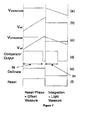
- Fig. 8 illustrates a first embodiment of a method of operating an image sensor, in which there are three phases, namely a reset phase, a calibration phase ("calibrate”) and an integration phase, which comprises sensor exposure and conversion of the incoming signal.
- the time for reset is not critical to this application - the minimum time is determined by how quickly the support circuitry can reset the pixel.
- the maximum time is determined by the system's frame rate. Typically, the system will use the shortest reset period possible to maximise the frame rate. A practical range for the reset period is 1 ⁇ s - 10 ⁇ s.
- Vphotodiode (a) will change during the calibrate phase, degrading the accuracy of the offset compensation.
- the Vref signal (b) ramps.
- the Vref signal moved across the full voltage swing of the pixel.
- the Vref signal moves by ⁇ Vref which is much less than the full voltage swing.
- the full voltage swing of the pixel may be 1V, while the value of ⁇ Vref may be 100mV, giving a 1:10 ratio of ⁇ Vref:V.
- This ratio can of course be of any suitable value depending on the particular sensor array and desired performance parameters. It has been found that a useful upper limit for the ratio is around 1:4.
- the system measures the voltage on the pixel by measuring the offset time 36 taken for the comparator to change state. This value is then stored.
- the pixel collects light causing the Vphotodiode line to discharge.
- the discharge rate is proportional to the illumination.
- the point at which the comparator output changes gives a time 38, which can be known as the "conversion time”. This is used as a measure of the light.
- the actual amount of light falling on the pixel is then the difference between the readout value and calibrate value. By subtracting the stored (calibrate figure) from readout value, the true illumination can be measured.
- This embodiment is suitable for use with a linear sensor, where the Vref signal is not used in the exposure phase.
- Fig. 9 illustrates a second embodiment of a method of operating an image sensor, which incorporates a reset phase, a calibration phase, an exposure phase and a conversion phase ("convert").
- the reset and calibration phases are similar to those of the first embodiment. However, the exposure and conversion phases are now treated independently rather than as a combined "integration" phase.
- This embodiment is suitable for use with an enhanced dynamic-range sensor.
- the illumination After exposure, the illumination is turned off and the Reference voltage then ramps between the black value and white value. Measuring the conversion time 42 for the comparator output to change gives a value for the illumination (including offset & kTC noise).
- the pixels could comprise an alternative light sensitive element, such as a phototransistor, rather than a photodiode.
- the comparator could in fact be engineered to have a set offset, so that it changes when the values of the voltages concerned differ by an amount corresponding to that offset.
Landscapes
- Engineering & Computer Science (AREA)
- Multimedia (AREA)
- Signal Processing (AREA)
- Transforming Light Signals Into Electric Signals (AREA)
Priority Applications (3)
| Application Number | Priority Date | Filing Date | Title |
|---|---|---|---|
| EP03256970A EP1530363B1 (de) | 2003-11-04 | 2003-11-04 | Verbesserungen in oder in Bezug auf Bildsensoren |
| DE60333757T DE60333757D1 (de) | 2003-11-04 | 2003-11-04 | Verbesserungen in oder in Bezug auf Bildsensoren |
| US10/978,223 US7502061B2 (en) | 2003-11-04 | 2004-10-29 | Method for image sensor calibration and associated devices |
Applications Claiming Priority (1)
| Application Number | Priority Date | Filing Date | Title |
|---|---|---|---|
| EP03256970A EP1530363B1 (de) | 2003-11-04 | 2003-11-04 | Verbesserungen in oder in Bezug auf Bildsensoren |
Publications (2)
| Publication Number | Publication Date |
|---|---|
| EP1530363A1 true EP1530363A1 (de) | 2005-05-11 |
| EP1530363B1 EP1530363B1 (de) | 2010-08-11 |
Family
ID=34429519
Family Applications (1)
| Application Number | Title | Priority Date | Filing Date |
|---|---|---|---|
| EP03256970A Expired - Lifetime EP1530363B1 (de) | 2003-11-04 | 2003-11-04 | Verbesserungen in oder in Bezug auf Bildsensoren |
Country Status (3)
| Country | Link |
|---|---|
| US (1) | US7502061B2 (de) |
| EP (1) | EP1530363B1 (de) |
| DE (1) | DE60333757D1 (de) |
Cited By (4)
| Publication number | Priority date | Publication date | Assignee | Title |
|---|---|---|---|---|
| WO2005088959A1 (en) * | 2004-03-08 | 2005-09-22 | Eastman Kodak Company | Imaging system with adjusted dark floor correction |
| GB2460260A (en) * | 2008-05-22 | 2009-11-25 | Isis Innovation | Image sensor |
| WO2013148833A1 (en) | 2012-03-30 | 2013-10-03 | Pixim, Inc. | Cmos image sensors implementing full frame digital correlated double sampling with global shutter |
| CN104427271A (zh) * | 2013-08-29 | 2015-03-18 | 索尼公司 | Cmos图像传感器和用压缩实施相关双采样的成像方法 |
Families Citing this family (36)
| Publication number | Priority date | Publication date | Assignee | Title |
|---|---|---|---|---|
| GB0412296D0 (en) * | 2004-06-02 | 2004-07-07 | Council Cent Lab Res Councils | Imaging device |
| JP2009510868A (ja) * | 2005-09-28 | 2009-03-12 | ノキア コーポレイション | 製造過程におけるカメラ特性の内部記憶装置 |
| JP2008017388A (ja) * | 2006-07-10 | 2008-01-24 | Olympus Corp | 固体撮像装置 |
| JP2008042298A (ja) * | 2006-08-02 | 2008-02-21 | Olympus Corp | 固体撮像装置 |
| GB2476079A (en) * | 2009-12-10 | 2011-06-15 | St Microelectronics | Optical navigation device with a light sensor that detects the device movements and the ambient light level. |
| GB0921644D0 (en) | 2009-12-10 | 2010-01-27 | St Microelectronics Res & Dev | Improvements in or relating to optical navigation devices |
| GB2482278A (en) * | 2010-04-13 | 2012-02-01 | St Microelectronics Res & Dev | Image sensor analogue to digital conversion (ADC) with ramp signal delay compensation |
| GB2480621A (en) | 2010-05-25 | 2011-11-30 | St Microelectronics | Calibration of optical navigation devices in ambient light conditions |
| JP5954997B2 (ja) * | 2012-01-18 | 2016-07-20 | キヤノン株式会社 | 固体撮像装置及びその駆動方法 |
| JP6108936B2 (ja) * | 2013-04-24 | 2017-04-05 | キヤノン株式会社 | 撮像装置、撮像システム、撮像装置の駆動方法 |
| US9813652B2 (en) | 2013-08-29 | 2017-11-07 | Sony Corporation | CMOS image sensor and imaging method implementing correlated double sampling and compression |
| US10419701B2 (en) * | 2017-06-26 | 2019-09-17 | Facebook Technologies, Llc | Digital pixel image sensor |
| US10686996B2 (en) | 2017-06-26 | 2020-06-16 | Facebook Technologies, Llc | Digital pixel with extended dynamic range |
| US10917589B2 (en) | 2017-06-26 | 2021-02-09 | Facebook Technologies, Llc | Digital pixel with extended dynamic range |
| US10598546B2 (en) | 2017-08-17 | 2020-03-24 | Facebook Technologies, Llc | Detecting high intensity light in photo sensor |
| US11393867B2 (en) | 2017-12-06 | 2022-07-19 | Facebook Technologies, Llc | Multi-photodiode pixel cell |
| US10708529B2 (en) | 2017-12-20 | 2020-07-07 | Semiconductor Components Industries, Llc | Image sensors with low-voltage transistors |
| US10969273B2 (en) | 2018-03-19 | 2021-04-06 | Facebook Technologies, Llc | Analog-to-digital converter having programmable quantization resolution |
| US11004881B2 (en) | 2018-04-03 | 2021-05-11 | Facebook Technologies, Llc | Global shutter image sensor |
| US11089210B2 (en) | 2018-06-11 | 2021-08-10 | Facebook Technologies, Llc | Configurable image sensor |
| US11089241B2 (en) | 2018-06-11 | 2021-08-10 | Facebook Technologies, Llc | Pixel cell with multiple photodiodes |
| US11906353B2 (en) | 2018-06-11 | 2024-02-20 | Meta Platforms Technologies, Llc | Digital pixel with extended dynamic range |
| US11463636B2 (en) | 2018-06-27 | 2022-10-04 | Facebook Technologies, Llc | Pixel sensor having multiple photodiodes |
| US10897586B2 (en) | 2018-06-28 | 2021-01-19 | Facebook Technologies, Llc | Global shutter image sensor |
| US10931884B2 (en) | 2018-08-20 | 2021-02-23 | Facebook Technologies, Llc | Pixel sensor having adaptive exposure time |
| US11956413B2 (en) | 2018-08-27 | 2024-04-09 | Meta Platforms Technologies, Llc | Pixel sensor having multiple photodiodes and shared comparator |
| US11595602B2 (en) | 2018-11-05 | 2023-02-28 | Meta Platforms Technologies, Llc | Image sensor post processing |
| US11102430B2 (en) | 2018-12-10 | 2021-08-24 | Facebook Technologies, Llc | Pixel sensor having multiple photodiodes |
| US11218660B1 (en) | 2019-03-26 | 2022-01-04 | Facebook Technologies, Llc | Pixel sensor having shared readout structure |
| US11943561B2 (en) | 2019-06-13 | 2024-03-26 | Meta Platforms Technologies, Llc | Non-linear quantization at pixel sensor |
| US11936998B1 (en) | 2019-10-17 | 2024-03-19 | Meta Platforms Technologies, Llc | Digital pixel sensor having extended dynamic range |
| US11902685B1 (en) | 2020-04-28 | 2024-02-13 | Meta Platforms Technologies, Llc | Pixel sensor having hierarchical memory |
| US11910114B2 (en) | 2020-07-17 | 2024-02-20 | Meta Platforms Technologies, Llc | Multi-mode image sensor |
| US11623236B2 (en) | 2020-08-07 | 2023-04-11 | Stmicroelectronics (Research & Development) Limited | Fluidic ejection device with optical blockage detector |
| US11956560B2 (en) | 2020-10-09 | 2024-04-09 | Meta Platforms Technologies, Llc | Digital pixel sensor having reduced quantization operation |
| US12022218B2 (en) | 2020-12-29 | 2024-06-25 | Meta Platforms Technologies, Llc | Digital image sensor using a single-input comparator based quantizer |
Citations (4)
| Publication number | Priority date | Publication date | Assignee | Title |
|---|---|---|---|---|
| EP0675345A2 (de) * | 1994-03-30 | 1995-10-04 | Nec Corporation | Einrichtung und Verfahren zum Lichtempfang, mit Verwendung in einem CCD-Bildsensor oder ähnlichem |
| US5479208A (en) * | 1993-03-25 | 1995-12-26 | Nec Corporation | Image sensors and driving method thereof |
| EP1081942A1 (de) * | 1999-08-31 | 2001-03-07 | General Electric Company | Offset- und Verstärkungskorrektursystem für Verstärker in einer Röntgenstrahlen-Bildaufnahmeeinheit |
| US6538695B1 (en) * | 1998-11-04 | 2003-03-25 | Ic Media Corporation | On-chip fixed-pattern noise calibration for CMOS image sensors |
Family Cites Families (15)
| Publication number | Priority date | Publication date | Assignee | Title |
|---|---|---|---|---|
| US7304670B1 (en) * | 1997-03-28 | 2007-12-04 | Hand Held Products, Inc. | Method and apparatus for compensating for fixed pattern noise in an imaging system |
| US5877715A (en) * | 1997-06-12 | 1999-03-02 | International Business Machines Corporation | Correlated double sampling with up/down counter |
| JPH11164210A (ja) * | 1997-11-28 | 1999-06-18 | Nikon Corp | 動き検出用固体撮像装置 |
| US6452633B1 (en) * | 1998-02-26 | 2002-09-17 | Foveon, Inc. | Exposure control in electronic cameras by detecting overflow from active pixels |
| US6366317B1 (en) * | 1998-03-27 | 2002-04-02 | Intel Corporation | Motion estimation using intrapixel logic |
| US6266373B1 (en) * | 1998-06-15 | 2001-07-24 | U.S. Philips Corporation | Pixel data storage system for use in half-pel interpolation |
| US6583817B1 (en) * | 1998-06-24 | 2003-06-24 | Taiwan Advanced Sensors Corp. | Autocalibration of the A/D converter within the CMOS type image sensor |
| US6704050B1 (en) * | 1999-04-23 | 2004-03-09 | Polaroid Corporation | Active-pixel image sensing device with linear mode voltage to current conversion |
| US6225852B1 (en) * | 1999-10-01 | 2001-05-01 | Advanced Micro Devices, Inc. | Use of biased high threshold voltage transistor to eliminate standby current in low voltage integrated circuits |
| KR100399954B1 (ko) * | 2000-12-14 | 2003-09-29 | 주식회사 하이닉스반도체 | 아날로그 상호 연관된 이중 샘플링 기능을 수행하는씨모스 이미지 센서용 비교 장치 |
| US6660989B2 (en) * | 2001-07-11 | 2003-12-09 | Texas Instruments Incorporated | CMOS imager having asynchronous pixel readout in order of pixel illumination |
| US6617565B2 (en) * | 2001-11-06 | 2003-09-09 | Omnivision Technologies, Inc. | CMOS image sensor with on-chip pattern recognition |
| US7280141B1 (en) * | 2003-09-23 | 2007-10-09 | Pixim Inc | Fixed pattern noise subtraction in a digital image sensor |
| JP4093220B2 (ja) * | 2004-10-05 | 2008-06-04 | コニカミノルタホールディングス株式会社 | 固体撮像装置及びこの固体撮像装置を備える撮像装置 |
| US20060077273A1 (en) * | 2004-10-12 | 2006-04-13 | Hae-Seung Lee | Low noise active pixel image sensor |
-
2003
- 2003-11-04 EP EP03256970A patent/EP1530363B1/de not_active Expired - Lifetime
- 2003-11-04 DE DE60333757T patent/DE60333757D1/de not_active Expired - Lifetime
-
2004
- 2004-10-29 US US10/978,223 patent/US7502061B2/en active Active
Patent Citations (4)
| Publication number | Priority date | Publication date | Assignee | Title |
|---|---|---|---|---|
| US5479208A (en) * | 1993-03-25 | 1995-12-26 | Nec Corporation | Image sensors and driving method thereof |
| EP0675345A2 (de) * | 1994-03-30 | 1995-10-04 | Nec Corporation | Einrichtung und Verfahren zum Lichtempfang, mit Verwendung in einem CCD-Bildsensor oder ähnlichem |
| US6538695B1 (en) * | 1998-11-04 | 2003-03-25 | Ic Media Corporation | On-chip fixed-pattern noise calibration for CMOS image sensors |
| EP1081942A1 (de) * | 1999-08-31 | 2001-03-07 | General Electric Company | Offset- und Verstärkungskorrektursystem für Verstärker in einer Röntgenstrahlen-Bildaufnahmeeinheit |
Cited By (10)
| Publication number | Priority date | Publication date | Assignee | Title |
|---|---|---|---|---|
| WO2005088959A1 (en) * | 2004-03-08 | 2005-09-22 | Eastman Kodak Company | Imaging system with adjusted dark floor correction |
| US7330208B2 (en) | 2004-03-08 | 2008-02-12 | Eastman Kodak Company | Electronic imaging system with adjusted dark floor correction |
| US7907192B2 (en) | 2004-03-08 | 2011-03-15 | Eastman Kodak Company | Electronic imaging system with adjusted dark floor correction |
| GB2460260A (en) * | 2008-05-22 | 2009-11-25 | Isis Innovation | Image sensor |
| WO2013148833A1 (en) | 2012-03-30 | 2013-10-03 | Pixim, Inc. | Cmos image sensors implementing full frame digital correlated double sampling with global shutter |
| CN104335573A (zh) * | 2012-03-30 | 2015-02-04 | 匹克希姆公司 | 实现伴随全局快门的全帧数字相关双采样的cmos图像传感器 |
| EP2832090A4 (de) * | 2012-03-30 | 2015-10-14 | Pixim Inc | Cmos-bildsensoren mit durch einen full-frame korrelierter doppelter signalabtastung und einer gesamtblende |
| CN104335573B (zh) * | 2012-03-30 | 2017-12-15 | 匹克希姆公司 | Cmos图像传感器及其方法 |
| CN104427271A (zh) * | 2013-08-29 | 2015-03-18 | 索尼公司 | Cmos图像传感器和用压缩实施相关双采样的成像方法 |
| CN104427271B (zh) * | 2013-08-29 | 2019-06-18 | 索尼公司 | Cmos图像传感器和用压缩实施相关双采样的成像方法 |
Also Published As
| Publication number | Publication date |
|---|---|
| US20050104983A1 (en) | 2005-05-19 |
| EP1530363B1 (de) | 2010-08-11 |
| DE60333757D1 (de) | 2010-09-23 |
| US7502061B2 (en) | 2009-03-10 |
Similar Documents
| Publication | Publication Date | Title |
|---|---|---|
| EP1530363B1 (de) | Verbesserungen in oder in Bezug auf Bildsensoren | |
| JP4037602B2 (ja) | ダイナミックレンジを拡大させるmos画像形成装置 | |
| US5920345A (en) | CMOS image sensor with improved fill factor | |
| CN109155827B (zh) | 高动态范围成像传感器阵列 | |
| US7920193B2 (en) | Methods, systems and apparatuses using barrier self-calibration for high dynamic range imagers | |
| EP2832090B1 (de) | Cmos-bildsensoren mit full-frame korrelierter doppelter signalabtastung und globalem verschluss | |
| US20110221931A1 (en) | Temperature information output apparatus, imaging apparatus, method of outputting temperature information | |
| US10200644B2 (en) | Global shutter scheme that reduces the effects of dark current | |
| US8520106B2 (en) | Solid-state imaging device with improved dynamic range | |
| EP2874388B1 (de) | Verfahren zur Vermeidung von Pixelsättigung | |
| KR20140103116A (ko) | 특히 시간 의존성 이미지 데이터의 비동기성 검출로 감지하는 샘플링된 밝기를 통합하기 위한 포토어레이 | |
| GB2328338A (en) | Temperature dependent dark current correction in imaging apparatus | |
| JP2011029887A (ja) | 撮像装置及び制御方法 | |
| JP4358351B2 (ja) | 光検出装置 | |
| JP3226859B2 (ja) | 撮像装置 | |
| US5027148A (en) | Autofocus chip with reference level determination circuit | |
| JP3022166B2 (ja) | 固体撮像素子 | |
| US7242429B1 (en) | Method for cancellation of the effect of charge feedthrough on CMOS pixel output | |
| JP2004356866A (ja) | 撮像装置 | |
| JP3212858B2 (ja) | 固体撮像装置 | |
| CN119421070B (zh) | 图像信号读出电路、图像信号读取方法及电子设备 | |
| CN114868379B (zh) | 光传感器 | |
| HK1262355A1 (en) | High dynamic range imaging sensor array | |
| HK1262355B (en) | High dynamic range imaging sensor array | |
| HK1186029A1 (zh) | 用於成像像素的黑色电平校正的方法和系统 |
Legal Events
| Date | Code | Title | Description |
|---|---|---|---|
| PUAI | Public reference made under article 153(3) epc to a published international application that has entered the european phase |
Free format text: ORIGINAL CODE: 0009012 |
|
| AK | Designated contracting states |
Kind code of ref document: A1 Designated state(s): AT BE BG CH CY CZ DE DK EE ES FI FR GB GR HU IE IT LI LU MC NL PT RO SE SI SK TR |
|
| AX | Request for extension of the european patent |
Extension state: AL LT LV MK |
|
| 17P | Request for examination filed |
Effective date: 20051028 |
|
| AKX | Designation fees paid |
Designated state(s): DE FR GB IT |
|
| RAP1 | Party data changed (applicant data changed or rights of an application transferred) |
Owner name: STMICROELECTRONICS (RESEARCH & DEVELOPMENT) LIMITE |
|
| GRAP | Despatch of communication of intention to grant a patent |
Free format text: ORIGINAL CODE: EPIDOSNIGR1 |
|
| GRAS | Grant fee paid |
Free format text: ORIGINAL CODE: EPIDOSNIGR3 |
|
| GRAA | (expected) grant |
Free format text: ORIGINAL CODE: 0009210 |
|
| AK | Designated contracting states |
Kind code of ref document: B1 Designated state(s): DE FR GB IT |
|
| REG | Reference to a national code |
Ref country code: GB Ref legal event code: FG4D |
|
| REF | Corresponds to: |
Ref document number: 60333757 Country of ref document: DE Date of ref document: 20100923 Kind code of ref document: P |
|
| PLBE | No opposition filed within time limit |
Free format text: ORIGINAL CODE: 0009261 |
|
| STAA | Information on the status of an ep patent application or granted ep patent |
Free format text: STATUS: NO OPPOSITION FILED WITHIN TIME LIMIT |
|
| 26N | No opposition filed |
Effective date: 20110512 |
|
| REG | Reference to a national code |
Ref country code: DE Ref legal event code: R079 Ref document number: 60333757 Country of ref document: DE Free format text: PREVIOUS MAIN CLASS: H04N0003150000 Ipc: H04N0005357000 |
|
| REG | Reference to a national code |
Ref country code: DE Ref legal event code: R079 Ref document number: 60333757 Country of ref document: DE Free format text: PREVIOUS MAIN CLASS: H04N0003150000 Ipc: H04N0005357000 Effective date: 20110802 Ref country code: DE Ref legal event code: R097 Ref document number: 60333757 Country of ref document: DE Effective date: 20110512 |
|
| REG | Reference to a national code |
Ref country code: FR Ref legal event code: PLFP Year of fee payment: 13 |
|
| REG | Reference to a national code |
Ref country code: FR Ref legal event code: PLFP Year of fee payment: 14 |
|
| REG | Reference to a national code |
Ref country code: FR Ref legal event code: PLFP Year of fee payment: 15 |
|
| REG | Reference to a national code |
Ref country code: FR Ref legal event code: PLFP Year of fee payment: 16 |
|
| REG | Reference to a national code |
Ref country code: DE Ref legal event code: R079 Ref document number: 60333757 Country of ref document: DE Free format text: PREVIOUS MAIN CLASS: H04N0005357000 Ipc: H04N0025600000 |
|
| PGFP | Annual fee paid to national office [announced via postgrant information from national office to epo] |
Ref country code: FR Payment date: 20221021 Year of fee payment: 20 |
|
| PGFP | Annual fee paid to national office [announced via postgrant information from national office to epo] |
Ref country code: IT Payment date: 20221020 Year of fee payment: 20 Ref country code: GB Payment date: 20221021 Year of fee payment: 20 Ref country code: DE Payment date: 20221020 Year of fee payment: 20 |
|
| REG | Reference to a national code |
Ref country code: DE Ref legal event code: R071 Ref document number: 60333757 Country of ref document: DE |
|
| REG | Reference to a national code |
Ref country code: GB Ref legal event code: PE20 Expiry date: 20231103 |
|
| PG25 | Lapsed in a contracting state [announced via postgrant information from national office to epo] |
Ref country code: GB Free format text: LAPSE BECAUSE OF EXPIRATION OF PROTECTION Effective date: 20231103 |
|
| PG25 | Lapsed in a contracting state [announced via postgrant information from national office to epo] |
Ref country code: GB Free format text: LAPSE BECAUSE OF EXPIRATION OF PROTECTION Effective date: 20231103 |