EP1540745B1 - Procede de production d'un boitier de composant a cadre de montage - Google Patents
Procede de production d'un boitier de composant a cadre de montage Download PDFInfo
- Publication number
- EP1540745B1 EP1540745B1 EP03747830.2A EP03747830A EP1540745B1 EP 1540745 B1 EP1540745 B1 EP 1540745B1 EP 03747830 A EP03747830 A EP 03747830A EP 1540745 B1 EP1540745 B1 EP 1540745B1
- Authority
- EP
- European Patent Office
- Prior art keywords
- leadframe
- injection
- housing
- recess
- radiation
- Prior art date
- Legal status (The legal status is an assumption and is not a legal conclusion. Google has not performed a legal analysis and makes no representation as to the accuracy of the status listed.)
- Expired - Lifetime
Links
Images



Classifications
-
- H—ELECTRICITY
- H10—SEMICONDUCTOR DEVICES; ELECTRIC SOLID-STATE DEVICES NOT OTHERWISE PROVIDED FOR
- H10H—INORGANIC LIGHT-EMITTING SEMICONDUCTOR DEVICES HAVING POTENTIAL BARRIERS
- H10H20/00—Individual inorganic light-emitting semiconductor devices having potential barriers, e.g. light-emitting diodes [LED]
- H10H20/80—Constructional details
- H10H20/85—Packages
- H10H20/8506—Containers
-
- H—ELECTRICITY
- H10—SEMICONDUCTOR DEVICES; ELECTRIC SOLID-STATE DEVICES NOT OTHERWISE PROVIDED FOR
- H10F—INORGANIC SEMICONDUCTOR DEVICES SENSITIVE TO INFRARED RADIATION, LIGHT, ELECTROMAGNETIC RADIATION OF SHORTER WAVELENGTH OR CORPUSCULAR RADIATION
- H10F77/00—Constructional details of devices covered by this subclass
- H10F77/50—Encapsulations or containers
-
- H—ELECTRICITY
- H10—SEMICONDUCTOR DEVICES; ELECTRIC SOLID-STATE DEVICES NOT OTHERWISE PROVIDED FOR
- H10H—INORGANIC LIGHT-EMITTING SEMICONDUCTOR DEVICES HAVING POTENTIAL BARRIERS
- H10H20/00—Individual inorganic light-emitting semiconductor devices having potential barriers, e.g. light-emitting diodes [LED]
- H10H20/80—Constructional details
- H10H20/85—Packages
- H10H20/857—Interconnections, e.g. lead-frames, bond wires or solder balls
-
- H—ELECTRICITY
- H10—SEMICONDUCTOR DEVICES; ELECTRIC SOLID-STATE DEVICES NOT OTHERWISE PROVIDED FOR
- H10W—GENERIC PACKAGES, INTERCONNECTIONS, CONNECTORS OR OTHER CONSTRUCTIONAL DETAILS OF DEVICES COVERED BY CLASS H10
- H10W90/00—Package configurations
- H10W90/701—Package configurations characterised by the relative positions of pads or connectors relative to package parts
- H10W90/751—Package configurations characterised by the relative positions of pads or connectors relative to package parts of bond wires
- H10W90/756—Package configurations characterised by the relative positions of pads or connectors relative to package parts of bond wires between a chip and a stacked lead frame, conducting package substrate or heat sink
Definitions
- the invention relates to a method for producing a leadframe-based component housing.
- the invention relates in particular to surface mounting on a printed circuit board suitable light-emitting diode devices in which a preferably formed as a reflector recess is provided with a directed toward the front of the component housing radiation window in a manufactured in the injection molding housing base body with partially embedded electrical connection strip.
- the recess, in which a chip emitting electromagnetic radiation is located, is filled, for example, with an encapsulation compound which is permeable to electromagnetic radiation emitted by the chip.
- Such device packages are also suitable for use with radiation-detecting chips - the radiation window must then be transparent to an electromagnetic radiation to be received by the chip.
- the invention is particularly suitable for use in radiation-emitting components, in which the chips are incorporated into pre-housed leadframes, so-called "premolded leadframes". This means that the leadframes are in each case encapsulated with a housing base body prior to assembly of the chip.
- the terminal strips are first partially punched into a leadframe band. Thereafter, the leadframe tape is inserted into a two-part mold, which forms a cavity around the leadframe to form the housing body.
- a spray nozzle for example, over the adjacent to the back of the leadframes part of the injection mold, that is, in the adjacent to the back of the leadframes part of the cavity a spray mass, z.
- a white plastic filled, and filled the entire cavity of the mold.
- the injection mold is opened.
- the spray mass located in the spray nozzle is torn off from the injection molding compound in the cavity.
- the chip is preferably arranged in the recess provided on one of the terminal strips, electrically conductively connected to the terminal strip and provided with the encapsulant. Subsequently, the components connected by the leadframe band can be separated from each other and thus separated from this composite.
- a radiation-emitting component of the type mentioned is for example in the EP 0 400 176 A1 described.
- the component has a housing base body with a bearing surface in which a leadframe (leadframe) is partially embedded. Parts of the leadframe are formed as terminal strips, which protrude from the housing base body and are bent in the further course, that their pads lie with the support surface, which determines the mounting plane of the device in a plane.
- the total height of the components produced in this way can be reduced, if at all, then only with great technical effort to less than about 1 mm.
- the minimum height of the front part of the housing base body is about 0.5 mm, the back wall of the housing base body about 0.3 mm and the thickness of the terminal strip about 0.1 mm.
- the layer thickness of the injection molding compound in the cavity between the leadframe and the tear-off point at the spray nozzle must be sufficiently large in order to largely prevent delamination between the leadframe backside and the sprayed compound. Such delamination would drastically increase the risk of damage to the device during further processing or later during operation.
- the above-mentioned layer thickness of the spray mass must be so large that the mechanical tensile forces occurring in the spray mass when tearing off the spray nozzle are reduced to such an extent that the forces acting on the border to the lead frame are insufficient to tear off the spray mass from the lead frame.
- the radiation-emitting components should have a significantly lower height.
- the ability to increase the device height by reducing the height of the housing body from the side of the chip is very limited due to a finite height of the radiation-emitting chip.
- the ability to achieve the stated goal by simply reducing the thickness of the housing body at the back of the leadframe is also severely limited because, as stated above, with too thin a layer of the molding compound that realizes the back of the housing , This is easily entrained in the spray process for the preparation of the housing with the spray nozzle to be removed, whereby the hermeticity of the component destroyed and thus the functioning of the device can be disturbed.
- the publication JP 11-340403 A shows the preamble of claim 1.
- a light-emitting semiconductor device and a production method thereof are in the document EP 0 854 523 A2 disclosed.
- the injection of the injection molding compound thus takes place from the back side of the lead frame through the injection window into the part of the cavity of the injection mold which produces the front part of the housing main body at the front side of the lead frame.
- the spray nozzle is guided to the injection window of the leadframe. In this way it is achieved that adjacent to the spray nozzle and thus to the tear region of the injection molding compound at the cavity-side end of the spray nozzle, a comparatively large injection mass volume with a comparatively large cross-section. The risk of delamination is reduced in this type of housing.
- the Anspritz window is preferably arranged in one of the electrical connection strips.
- the rear wall that is to say the plastic wall between the rear side of the leadframe and the rear side of the housing main body, is advantageously with a thickness of 0.3 mm or less, preferably 0.25 mm or less, particularly preferably 0.2 mm or less it being understood that the thickness in each. Case is greater than 0 mm.
- the invention is suitable for use in components in which in the front part of the housing main body at least one recess for receiving a chip, in particular a radiation-emitting or radiation-detecting semiconductor chip, for. B. a light emitting diode, is provided.
- the An mousse window is in this case arranged in the region of a wall bounding the recess wall of the front part.
- a chip mounting surface is provided, which is preferably located on one of the two terminal strips, but can also be arranged on the housing base body.
- a chip mounting surface can also be provided later, for example in the form of a carrier plate to be subsequently inserted into the recess.
- a thermal connection socket is used, which preferably extends from the bottom of the recess through the housing base body to the rear side.
- the recess has a radiation exit window.
- the inner surfaces of the recess are in this case preferably designed as a radiation reflector.
- the injection molding compound preferably has a plastic, in particular a temperature-resistant, filled with white filler plastic.
- the plastic is preferably thermoplastic material, and the filler is preferably titanium oxide and / or barium sulfate.
- reaction resins such as epoxy resins, acrylic resins, silicone resins and polyurethane resins
- epoxy resins acrylic resins, silicone resins and polyurethane resins
- the Anspritz window is in a housing base body with recess for the chip particularly preferably below a recess at least partially enclosing solid wall of the housing base body.
- the particular advantage of the manufacturing method according to the invention is that the overall height of a thus produced component housing can be substantially reduced by the particularly thin formed rear wall of the component housing, in particular over the previously known radiation-emitting components, which are produced by pre-housed lead frames.
- the term “leadframe” refers in particular to metallic leadframes, as are conventionally used in semiconductor optoelectronics, for example for light-emitting diode housings.
- the term “leadframe” also includes all other leadframes which are suitable for the housing technology according to the invention and which do not necessarily have to be completely metallic and can, for example, comprise a combination of electrically insulating material and electrical conductor tracks applied thereto.
- Leadframe is not necessarily a continuous band that is suitable for a "reel to reel” technique. Rather, the leadframe may be e.g. also in the form of stripes or arrays.
- FIG. 1 shows a perspective view of a surface mount device with a housing according to the prior art.
- FIG. 1 shown, rectangular in outline housing body 100 has a front part 8a and a rear wall 8b, wherein in the front part 8a, a reflector recess is provided with a radiation exit window 12.
- a first terminal strip 2a and a second terminal strip 2b are partially embedded in the housing main body and connected to a radiation-emitting chip, not shown here (hidden inside the housing main body).
- the protruding parts of the terminal strip are used to contact the device, for. B. to an external circuit board. It is possible that the external contacts are perpendicular to the corresponding side wall of the housing or, as with a dashed line in FIG. 1 indicated, bent around the housing body.
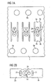
- the leadframe tape 1 according to the embodiment of FIGS. 2a and 2b is z. B. pre-structured by punching and in particular has a plurality of first terminal strip 2a and a plurality of second terminal strip 2b, which are separated in a later step from the leadframe tape along the lines 3a and 3b.
- the terminal strips 2a and 2b are provided as cathode or anode terminals of the components to be manufactured.
- further structures for example heat-dissipating strips
- a chip mounting surface 14 for a chip or on the terminal strip 2b a wire pad 13 is provided for a bonding wire in this embodiment.
- a Anspritz window 24 is provided, in which when forming a housing base in the injection molding a Spray nozzle is insertable.
- the Anspritz window may be provided in the second terminal strip 2b. It is expedient that the Anspritz window are each provided below a side wall to be formed later of the housing base body.
- the chip mounting surface 14 or the wire connection surface 13 of the leadframe band protrude (in the finished housing base body) into a reflector recess provided or adjoin a surface at least to the interior of the recess and then form at least part of the bottom surface of the recess.
- a separate recess may additionally be formed in the reflector recess, which leads to the wire connection region.
- Circular openings 6a and 6b are also formed in the leadframe band 1, through which the leadframe band can be guided and transported.
- the terminal strips 2a and 2b also have preferably rectangular openings 21, which for the discharge of the component housing during bending of the terminal strip (see FIG. 1 ) or for anchoring the terminal strip in the component housing are suitable.
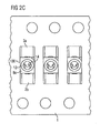
- Figure 2c shows the leadframe tape 1 with housing basic bodies 100 produced by means of a spraying process, each having a chip mounting surface 14 and a respective recess leading to this chip mounting surface.
- FIG. 3a embodiment shown for a leadframe of a housing or component having a substantially circular outline has sickle-shaped terminal strip, which on the one hand for better anchoring of the terminal strip in the housing base body and on the other hand to a resilient strain relief in bending the terminal strip is used.
- This leadframe also has an injection window 24, which is arranged next to a chip mounting surface 14, into or onto which an injection nozzle can be inserted or brought from the rear side of the leadframe for producing the housing main body.
- FIG. 3b shows a housing main body 100 with a substantially circular outline in a perspective view from below.
- the Anspritz window 24 through which the housing base body 100 is injected into the cavity of a corresponding injection mold in the adjacent to the front of the leadframe part of the cavity.
- the front part of the housing main body 100 is, for example, as in FIG Figure 3c shown designed.
- This type of housing is particularly suitable for the production of surface-mountable radiation-emitting and / or radiation-detecting components with Leuchtdioden- and / or photodiode chips, which are at least partially retractable in circular breakthroughs of printed circuit boards or the like.
- FIG. 3b shown component is in Figure 3c shown in perspective view.
- a radiation-emitting chip 16 for example a light-emitting diode chip, is fastened in a reflector opening, for example on the connection strip 2a.
- As connecting means for example, a metallic solder or a conductive adhesive is used.
- a second contact of the LED chip is electrically connected to the terminal strip 2b, for example by means of a bonding wire 17a.
- the side wall 11 of a recess which connects the bottom surface of the recess with the outer surface of the housing main body 100, is designed such that it acts as a reflector surface for a radiated from the chip 16 electromagnetic radiation. It can be flat, concave or otherwise appropriately shaped depending on the desired radiation behavior.
- visible projections 10a, 10b and 10c of the housing main body serve to guide the lying outside of the housing main body terminal strip. In addition, they can also serve as insertion bevels for inserting the housing into platinum openings.
- the chip 16 On the front side facing away from the terminal strip, the chip 16 has a contact surface, from which an electrical connection line 17 (eg, a wire connection) is guided to the wire connection part 13.
- an electrical connection line 17 eg, a wire connection
- the front part 8a of the housing main body 100 which is provided, for example, for later installation of a light-emitting diode chip, in both cases has a reflector recess in the form of a frustoconical opening which widens in the direction of the main emission direction and has a radiation exit window 12.
- the reflector recess is filled with a transparent encapsulation compound 41.
- a chip 16 to be used in a later method step and an electrical connection line 17 are shown schematically by dashed lines.
- the inclined side surface 11 of the recess preferably serves as a reflector.
- a two-part or multi-part injection mold with a cavity for the housing main body 100 is used, in which the leadframe is inserted during the spraying process.
- the cavity of the injection mold is filled by means of a spray nozzle 23 with a spray mass for the housing main body.
- the spray mass is injected into the volume adjacent to the rear side of the lead frame. After curing of the spray mass, the spray nozzle is separated from the injection mold. When separating the spray nozzle of the area near the separation point of a strong mechanical stress is exposed to the delamination of the material of the (cured) spray mass at the interface between the rear wall 8b of the housing base body and the terminal strip 2a and 2b. Therefore, at a small height of the rear wall 8b, these are easily damaged. In order to avoid this as far as possible, a comparatively large thickness of the rear wall 8b of the housing main body is required.
- the spray nozzle 23 is not introduced in the middle region of a cavity suitable for forming the rear wall 8b of the housing main body, but is applied to a molded-on window 24 arranged laterally in the leadframe or introduced into the injection window 24.
- the separation point 25 is not opposite to the leadframe, but adjacent to the mass of the spray mass of the solidly formed side wall of the housing body.
- Such a device is particularly suitable for flat display modules or as backlight, For example, for a liquid crystal display, suitable.
- FIGS. 5a and 5b In each case, an injection mold 200, which has a cavity 210, is shown.
- electrical pads 20a and 20b of the terminal strips 2a and 2b which are provided for an electrically conductive contacting of a chip with the terminal strips 2a and 2b, are not covered with spatter.
- the spray mass is sprayed by means of the spray nozzle 23 from below against the terminal strips 2a, 2b, so that the terminal strips 2a, 2b are pressed with the electrical pads 20a and 20b against the injection mold (course of the spray during injection is indicated by arrows).
- the pads 20a, 20b are largely sealed during the transfer molding and the risk of covering the pads 20a, 20b reduced with spray mass.
- an injection mold 200 for a component package according to the method of the invention as shown in FIG. 5b is shown, the injection molding compound injected via the injection window 24 in the cavity 210 that a pressing of the pads 20a and 20b to the injection mold, as it is formed in the preceding paragraph, does not take place. Rather, there is a risk that the terminal strips 2a, 2b and thus the pads 20a, 20b are pushed away from the injection mold and forms a gap between the upper inner wall of the injection mold and the pads 20a, 20b, which then covers the pads 20a, 20b causes (course of the injection compound during injection is again indicated by arrows).
- an injection mold 200 (see FIG. 5b) is designed in such a way that it also opens when the connection strips 2a, 2b are clamped the surfaces opposite the pads 20a, 20b of the terminal strips 2a, 2b with an inner side.
- the terminal strips 2a, 2b in a region of the pads 20a, 20b are pressed against the associated inner wall of the injection mold such that they are sealed.
- a housing base body produced with such an injection mold 200 has recesses in the rear wall of the housing main body in areas of the connection strips 2a, 2b which lie opposite the connection surfaces 20a, 20b.
- the exposed in these areas to the outside surfaces of the terminal strips 2a, 2b can be subsequently electrically insulated from the outside. This can be done for example by coating with an electrically insulating material, such as electrically insulating paint.
Landscapes
- Led Device Packages (AREA)
- Injection Moulding Of Plastics Or The Like (AREA)
Claims (6)
- Procédé de fabrication d'un boîtier à base de grille de connexion pour un composant électronique pouvant être monté en surface comportant une grille de connexion présentant une face avant et une face arrière, qui présente au moins deux bandes de raccordement électrique (2a, 2b), et un bâti de boîtier (8a, 8b) moulé par injection ou par transfert et constitué d'une masse d'injection électriquement isolante qui présente une partie avant (8a) disposée sur la face avant de la grille de connexion et une paroi arrière (8b) disposée sur la face arrière de la grille de connexion, dans lequel la grille de connexion présente au moins une fenêtre d'injection (24) à travers laquelle le bâti de boîtier est injecté sur la grille de connexion à partir d'une face arrière de la grille de connexion,
comportant les étapes de procédé suivantes :- fourniture de la grille de connexion comportant les deux bandes de raccordement (2a, 2b) et la fenêtre d'injection (24),- application sur la grille de connexion d'un moule d'injection (200) qui forme une cavité autour de la grille de connexion pour la réalisation du bâti de boîtier (8a, 8b), et introduction ou application d'une buse d'injection (23) dans ou sur la fenêtre d'injection (24),- injection de la masse d'injection dans la cavité,- durcissement au moins partiel de la masse d'injection, et- ouverture du moule d'injection (200) tout en retirant la buse d'injection (23),caractérisé en ce que
la buse d'injection (23), lors de l'injection à travers une partie de la cavité créant une partie de paroi arrière du bâti de boîtier (8a, 8b) sur la face arrière de la grille de connexion, est guidée vers la fenêtre d'injection (24) de la grille de connexion. - Procédé selon la revendication précédente, dans lequel un matériau thermoplastique est utilisé en tant que masse d'injection.
- Procédé selon l'une des revendications précédentes, dans lequel la fenêtre d'injection (24) est disposée dans l'une des bandes de raccordement électrique (2a, 2b).
- Procédé selon l'une des revendications précédentes, dans lequel la paroi arrière est créée avec une épaisseur inférieure à 0,3 mm et supérieure à 0 mm.
- Procédé selon l'une des revendications précédentes, dans lequel un évidemment est formé dans le bâti de boîtier (8a, 8b) dans la partie avant (8a) pour la réception d'une puce d'émission de rayonnement et/ou de détection de rayonnement, dans lequel la fenêtre d'injection (24) est disposée dans la région d'une paroi de la partie avant (8a) délimitant l'évidemment.
- Procédé selon l'une des revendications précédentes, dans lequel l'évidemment est réalisé sous la forme d'un réflecteur.
Applications Claiming Priority (3)
| Application Number | Priority Date | Filing Date | Title |
|---|---|---|---|
| DE10243247 | 2002-09-17 | ||
| DE10243247A DE10243247A1 (de) | 2002-09-17 | 2002-09-17 | Leadframe-basiertes Bauelement-Gehäuse, Leadframe-Band, oberflächenmontierbares elektronisches Bauelement und Verfahren zur Herstellung |
| PCT/DE2003/002953 WO2004027882A2 (fr) | 2002-09-17 | 2003-09-05 | Boitier de composant a cadre de montage, bande de cadre de montage, composant electronique montable en surface et procede de production |
Publications (2)
| Publication Number | Publication Date |
|---|---|
| EP1540745A2 EP1540745A2 (fr) | 2005-06-15 |
| EP1540745B1 true EP1540745B1 (fr) | 2014-10-29 |
Family
ID=31969180
Family Applications (1)
| Application Number | Title | Priority Date | Filing Date |
|---|---|---|---|
| EP03747830.2A Expired - Lifetime EP1540745B1 (fr) | 2002-09-17 | 2003-09-05 | Procede de production d'un boitier de composant a cadre de montage |
Country Status (7)
| Country | Link |
|---|---|
| US (1) | US7102213B2 (fr) |
| EP (1) | EP1540745B1 (fr) |
| JP (1) | JP4351631B2 (fr) |
| CN (1) | CN100449798C (fr) |
| DE (1) | DE10243247A1 (fr) |
| TW (1) | TWI257692B (fr) |
| WO (1) | WO2004027882A2 (fr) |
Families Citing this family (75)
| Publication number | Priority date | Publication date | Assignee | Title |
|---|---|---|---|---|
| WO2005056269A2 (fr) * | 2003-12-09 | 2005-06-23 | G.L.I. Global Light Industries Gmbh | Procede pour produire des diodes electroluminescentes a semi-conducteurs sur une platine, et unites lumineuses a platine integree |
| DE102004033533B4 (de) * | 2004-07-09 | 2007-06-21 | G.L.I. Global Light Industries Gmbh | Leuchteinheit mit integrierter Platine |
| TWI237409B (en) * | 2004-10-08 | 2005-08-01 | Kingbright Electronics Co Ltd | Method of fabricating light emitting diode (LED) |
| US7821023B2 (en) | 2005-01-10 | 2010-10-26 | Cree, Inc. | Solid state lighting component |
| US9793247B2 (en) | 2005-01-10 | 2017-10-17 | Cree, Inc. | Solid state lighting component |
| US9070850B2 (en) | 2007-10-31 | 2015-06-30 | Cree, Inc. | Light emitting diode package and method for fabricating same |
| DE102005036520A1 (de) * | 2005-04-26 | 2006-11-09 | Osram Opto Semiconductors Gmbh | Optisches Bauteil, optoelektronisches Bauelement mit dem Bauteil und dessen Herstellung |
| KR100616684B1 (ko) | 2005-06-03 | 2006-08-28 | 삼성전기주식회사 | 고출력 led 패키지 및 그 제조방법 |
| US8669572B2 (en) | 2005-06-10 | 2014-03-11 | Cree, Inc. | Power lamp package |
| US8044412B2 (en) | 2006-01-20 | 2011-10-25 | Taiwan Semiconductor Manufacturing Company, Ltd | Package for a light emitting element |
| US7675145B2 (en) | 2006-03-28 | 2010-03-09 | Cree Hong Kong Limited | Apparatus, system and method for use in mounting electronic elements |
| EP1848042A1 (fr) * | 2006-04-21 | 2007-10-24 | LEXEDIS Lighting GmbH | Boîtier de DEL avec embase |
| US8748915B2 (en) | 2006-04-24 | 2014-06-10 | Cree Hong Kong Limited | Emitter package with angled or vertical LED |
| US7635915B2 (en) * | 2006-04-26 | 2009-12-22 | Cree Hong Kong Limited | Apparatus and method for use in mounting electronic elements |
| WO2007135707A1 (fr) | 2006-05-18 | 2007-11-29 | Nichia Corporation | Corps moulé en résine et dispositif électroluminescent monté en surface, procédé de fabrication correspondant |
| US8735920B2 (en) | 2006-07-31 | 2014-05-27 | Cree, Inc. | Light emitting diode package with optical element |
| US8367945B2 (en) | 2006-08-16 | 2013-02-05 | Cree Huizhou Opto Limited | Apparatus, system and method for use in mounting electronic elements |
| DE112007001950T5 (de) | 2006-08-21 | 2009-07-02 | Innotec Corporation, Zeeland | Elektrische Vorrichtung mit platinenloser Montageanordnung für elektrische Komponenten |
| US9711703B2 (en) | 2007-02-12 | 2017-07-18 | Cree Huizhou Opto Limited | Apparatus, system and method for use in mounting electronic elements |
| US7633055B2 (en) * | 2007-03-08 | 2009-12-15 | Lumination Llc | Sealed light emitting diode assemblies including annular gaskets and methods of making same |
| US8408773B2 (en) | 2007-03-19 | 2013-04-02 | Innotec Corporation | Light for vehicles |
| US7712933B2 (en) | 2007-03-19 | 2010-05-11 | Interlum, Llc | Light for vehicles |
| US8581278B2 (en) * | 2007-04-06 | 2013-11-12 | Kingbright Electronic Co., Ltd. | Light-emitting diode packaging structure |
| CN100487310C (zh) * | 2007-07-06 | 2009-05-13 | 深圳市泓亚光电子有限公司 | Led平板式多芯大功率光源 |
| US10256385B2 (en) | 2007-10-31 | 2019-04-09 | Cree, Inc. | Light emitting die (LED) packages and related methods |
| US8866169B2 (en) | 2007-10-31 | 2014-10-21 | Cree, Inc. | LED package with increased feature sizes |
| USD615504S1 (en) | 2007-10-31 | 2010-05-11 | Cree, Inc. | Emitter package |
| EP2232592B1 (fr) | 2007-12-12 | 2013-07-17 | Innotec Corporation | Procédé de surmouler une carte de circuit |
| USD633631S1 (en) | 2007-12-14 | 2011-03-01 | Cree Hong Kong Limited | Light source of light emitting diode |
| USD634863S1 (en) | 2008-01-10 | 2011-03-22 | Cree Hong Kong Limited | Light source of light emitting diode |
| JP2009238970A (ja) * | 2008-03-27 | 2009-10-15 | Panasonic Corp | 半導体装置用パッケージと光半導体装置 |
| US8049230B2 (en) | 2008-05-16 | 2011-11-01 | Cree Huizhou Opto Limited | Apparatus and system for miniature surface mount devices |
| JP5464825B2 (ja) * | 2008-07-23 | 2014-04-09 | ローム株式会社 | Ledモジュール |
| DE102008048259B4 (de) * | 2008-09-22 | 2024-10-02 | OSRAM Opto Semiconductors Gesellschaft mit beschränkter Haftung | Gehäuse für ein optoelektronisches Bauteil, seitlich emittierendes Bauteil mit einem Gehäuse und Verfahren zur Herstellung eines Gehäuses |
| US9425172B2 (en) | 2008-10-24 | 2016-08-23 | Cree, Inc. | Light emitter array |
| US8791471B2 (en) | 2008-11-07 | 2014-07-29 | Cree Hong Kong Limited | Multi-chip light emitting diode modules |
| US8368112B2 (en) * | 2009-01-14 | 2013-02-05 | Cree Huizhou Opto Limited | Aligned multiple emitter package |
| US20110037083A1 (en) * | 2009-01-14 | 2011-02-17 | Alex Chi Keung Chan | Led package with contrasting face |
| WO2010092853A1 (fr) * | 2009-02-10 | 2010-08-19 | 三洋電機株式会社 | Procédé de fabrication de boîtier à cadre |
| US8610156B2 (en) * | 2009-03-10 | 2013-12-17 | Lg Innotek Co., Ltd. | Light emitting device package |
| TWI485878B (zh) * | 2009-04-01 | 2015-05-21 | 光寶科技股份有限公司 | 形成發光二極體之透鏡結構之方法及其相關架構 |
| US8415692B2 (en) | 2009-07-06 | 2013-04-09 | Cree, Inc. | LED packages with scattering particle regions |
| US8598809B2 (en) | 2009-08-19 | 2013-12-03 | Cree, Inc. | White light color changing solid state lighting and methods |
| USD622232S1 (en) * | 2009-10-26 | 2010-08-24 | Foxsemicon Integrated Technology, Inc. | Light emitting diode |
| USD624884S1 (en) * | 2009-10-26 | 2010-10-05 | Foxsemicon Integrated Technology, Inc. | Light emitting diode |
| US20110101062A1 (en) * | 2009-11-04 | 2011-05-05 | Benjamin Franklin Roberts | Pouch and pouches to carry personal items and lights on a belt |
| KR101193909B1 (ko) * | 2009-12-31 | 2012-10-29 | 장광균 | Led 조명용 리드 프레임 및 그 제조방법 |
| USD627314S1 (en) * | 2010-02-01 | 2010-11-16 | Foxsemicon Integrated Technology, Inc. | Light-emitting diode |
| USD627312S1 (en) * | 2010-02-01 | 2010-11-16 | Foxsemicon Integrated Technology, Inc. | Light-emitting diode |
| USD627313S1 (en) * | 2010-02-01 | 2010-11-16 | Foxsemicon Integrated Technology, Inc. | Light-emitting diode |
| USD651183S1 (en) * | 2010-02-01 | 2011-12-27 | Foxsemicon Integrated Technology, Inc. | Light-emitting diode |
| USD627311S1 (en) * | 2010-02-01 | 2010-11-16 | Foxsemicon Integrated Technology, Inc. | Light-emitting diode |
| DE102010012039A1 (de) * | 2010-03-19 | 2011-09-22 | Osram Opto Semiconductors Gmbh | Optoelektronisches Bauelement und Verfahren zu dessen Herstellung |
| WO2011122665A1 (fr) | 2010-03-30 | 2011-10-06 | 大日本印刷株式会社 | Conducteur-poutre ou substrat destiné à une diode électroluminescente, dispositif à semi-conducteur et procédé de fabrication de conducteur-poutre ou de substrat destiné à une diode électroluminescente |
| US9012938B2 (en) | 2010-04-09 | 2015-04-21 | Cree, Inc. | High reflective substrate of light emitting devices with improved light output |
| US8933548B2 (en) | 2010-11-02 | 2015-01-13 | Dai Nippon Printing Co., Ltd. | Lead frame for mounting LED elements, lead frame with resin, method for manufacturing semiconductor devices, and lead frame for mounting semiconductor elements |
| US10043960B2 (en) * | 2011-11-15 | 2018-08-07 | Cree, Inc. | Light emitting diode (LED) packages and related methods |
| US8564004B2 (en) | 2011-11-29 | 2013-10-22 | Cree, Inc. | Complex primary optics with intermediate elements |
| JP5857709B2 (ja) * | 2011-12-14 | 2016-02-10 | 日産自動車株式会社 | 半導体装置 |
| JP5885493B2 (ja) * | 2011-12-21 | 2016-03-15 | 住友化学株式会社 | 半導体用パッケージ及び半導体発光装置 |
| DE112013002944T5 (de) | 2012-06-13 | 2015-02-19 | Innotec, Corp. | Flexibler Hohllichtleiter |
| JP6244873B2 (ja) * | 2013-12-16 | 2017-12-13 | 三菱電機株式会社 | 映像表示ユニットおよび発光装置 |
| US9601670B2 (en) | 2014-07-11 | 2017-03-21 | Cree, Inc. | Method to form primary optic with variable shapes and/or geometries without a substrate |
| US10622522B2 (en) | 2014-09-05 | 2020-04-14 | Theodore Lowes | LED packages with chips having insulated surfaces |
| WO2017005704A1 (fr) * | 2015-07-08 | 2017-01-12 | Firecomms Limited | Dispositif optoélectronique |
| DE102015214588A1 (de) * | 2015-07-31 | 2017-02-02 | Robert Bosch Gmbh | Anordnung zum Messen einer Drehzahl, insbesondere eines Turboladers eines Kraftfahrzeugs |
| CN106571383B (zh) | 2015-10-08 | 2020-04-28 | 联华电子股份有限公司 | 半导体元件及其制作方法 |
| USD799103S1 (en) * | 2016-05-20 | 2017-10-03 | Heptagon Micro Optics Pte. Ltd. | Optical emitter module |
| DE102017110850B4 (de) * | 2017-05-18 | 2024-12-05 | OSRAM Opto Semiconductors Gesellschaft mit beschränkter Haftung | Optoelektronisches Bauelement und Verfahren zum Herstellen eines optoelektronischen Bauelements |
| DE102017112642A1 (de) * | 2017-06-08 | 2018-12-13 | Osram Opto Semiconductors Gmbh | Led-filament |
| WO2019007513A1 (fr) * | 2017-07-06 | 2019-01-10 | Osram Opto Semiconductors Gmbh | Procédé de production d'un composant optoélectronique et composant optoélectronique |
| DE102017127621A1 (de) * | 2017-11-22 | 2019-05-23 | Osram Opto Semiconductors Gmbh | Vorrichtung mit Leiterrahmen und Verfahren zur Herstellung einer Mehrzahl von Vorrichtungen |
| CN114364913B (zh) * | 2018-12-17 | 2025-10-28 | 克鲁斯有限公司 | 符合ac驱动功率的条带照明系统 |
| US11592166B2 (en) | 2020-05-12 | 2023-02-28 | Feit Electric Company, Inc. | Light emitting device having improved illumination and manufacturing flexibility |
| US11876042B2 (en) | 2020-08-03 | 2024-01-16 | Feit Electric Company, Inc. | Omnidirectional flexible light emitting device |
Family Cites Families (11)
| Publication number | Priority date | Publication date | Assignee | Title |
|---|---|---|---|---|
| CA1195782A (fr) * | 1981-07-06 | 1985-10-22 | Mikio Nishikawa | Cadre de montage pour dispositif a semiconducteur encapsule de plastique |
| JPS58147141A (ja) | 1982-02-26 | 1983-09-01 | Nec Corp | 電子部品 |
| US4791472A (en) * | 1985-09-23 | 1988-12-13 | Hitachi, Ltd. | Lead frame and semiconductor device using the same |
| DE3623419A1 (de) * | 1986-07-11 | 1988-01-21 | Junghans Uhren Gmbh | Verfahren zum bestuecken eines leiterbahnen-netzwerkes fuer den schaltungstraeger eines elektromechanischen uhrwerks und teilbestuecktes leiterbahnen-netzwerk eines uhrwerks-schaltungstraegers |
| EP1022787B2 (fr) * | 1989-05-31 | 2012-07-11 | OSRAM Opto Semiconductors GmbH | Procédé de production d'un élément optique fixable sur une surface et élément optique fixable sur une surface |
| DE69427865T2 (de) | 1994-12-16 | 2002-04-11 | Seiko Epson Corp., Tokio/Tokyo | Halbleiteranordnung mit einer Wärmesenke und Herstellungsverfahren der Wärmesenke |
| US6274890B1 (en) | 1997-01-15 | 2001-08-14 | Kabushiki Kaisha Toshiba | Semiconductor light emitting device and its manufacturing method |
| JPH11340403A (ja) | 1998-05-28 | 1999-12-10 | Sony Corp | リードフレーム |
| DE10117889A1 (de) * | 2001-04-10 | 2002-10-24 | Osram Opto Semiconductors Gmbh | Leiterrahmen und Gehäuse für ein strahlungsemittierendes Bauelement, strahlungsemittierendes Bauelement sowie Verfahren zu dessen Herstellung |
| JP4388806B2 (ja) * | 2001-08-21 | 2009-12-24 | オスラム オプト セミコンダクターズ ゲゼルシャフト ミット ベシュレンクテル ハフツング | 放射線放出構成部材のためのケーシング及び導体フレーム、放射線放出構成部材、放射線放出構成部材を備えたディスプレイ装置及び/又は照明装置 |
| DE10140831A1 (de) * | 2001-08-21 | 2003-03-13 | Osram Opto Semiconductors Gmbh | Leiterrahmen und Gehäuse für ein strahlungsemittierendes Bauelement, strahlungsemittierendes Bauelement und Anzeige- und/oder Beleuchtungsanordnung mit strahlungsemittierenden Bauelementen |
-
2002
- 2002-09-17 DE DE10243247A patent/DE10243247A1/de not_active Withdrawn
-
2003
- 2003-09-05 CN CNB038220679A patent/CN100449798C/zh not_active Expired - Lifetime
- 2003-09-05 US US10/527,836 patent/US7102213B2/en not_active Expired - Lifetime
- 2003-09-05 EP EP03747830.2A patent/EP1540745B1/fr not_active Expired - Lifetime
- 2003-09-05 WO PCT/DE2003/002953 patent/WO2004027882A2/fr not_active Ceased
- 2003-09-05 JP JP2004536842A patent/JP4351631B2/ja not_active Expired - Lifetime
- 2003-09-16 TW TW092125466A patent/TWI257692B/zh not_active IP Right Cessation
Also Published As
| Publication number | Publication date |
|---|---|
| US20060157828A1 (en) | 2006-07-20 |
| WO2004027882A3 (fr) | 2004-07-29 |
| TWI257692B (en) | 2006-07-01 |
| EP1540745A2 (fr) | 2005-06-15 |
| WO2004027882A2 (fr) | 2004-04-01 |
| CN1682383A (zh) | 2005-10-12 |
| JP4351631B2 (ja) | 2009-10-28 |
| JP2005539386A (ja) | 2005-12-22 |
| CN100449798C (zh) | 2009-01-07 |
| TW200406892A (en) | 2004-05-01 |
| DE10243247A1 (de) | 2004-04-01 |
| US7102213B2 (en) | 2006-09-05 |
Similar Documents
| Publication | Publication Date | Title |
|---|---|---|
| EP1540745B1 (fr) | Procede de production d'un boitier de composant a cadre de montage | |
| EP1004145B1 (fr) | Composant optoelectronique | |
| DE69932268T2 (de) | Halbleiteranordnung aus vergossenem Kunststoff und Verfahren zu Ihrer Herstellung | |
| EP2396832B1 (fr) | Dispositif semi-conducteur optoélectronique encapsulé à couche d'arrêt brasée, et procédé correspondant | |
| EP1516372B1 (fr) | Diode luminescente et/ou photodiode montee en surface et procede de fabrication associe | |
| DE102013205894B4 (de) | Formgehäuse und Leuchtbauelement | |
| DE10237084A1 (de) | Verfahren zum Herstellen eines elektrischen Leiterrahmens und Verfahren zum Herstellen eines oberflächenmontierbaren Halbleiterbauelements | |
| WO1998015004A1 (fr) | Module puce en particulier pour implantation dans un corps de carte a puce | |
| EP2583318A1 (fr) | Composant optoélectronique pouvant être monté en surface et procédé de fabrication d'un composant optoélectronique pouvant être monté en surface | |
| WO2017032772A1 (fr) | Composant laser et procédé de réalisation | |
| WO2016202917A1 (fr) | Procédé de fabrication d'un composant optoélectronique et composant optoélectronique | |
| EP1525619A1 (fr) | Composant a semiconducteur pour montage en surface et procede de fabrication | |
| WO2015040107A1 (fr) | Composant optoélectronique et procédé de fabrication de celui-ci | |
| WO2004015769A1 (fr) | Procede pour realiser un cadre electriquement conducteur et procede pour realiser un composant semi-conducteur qui peut etre monte en surface, et strie de cadre conducteur | |
| WO2012031932A1 (fr) | Procédé de fabrication d'un composant semi-conducteur optoélectronique | |
| WO2014049059A2 (fr) | Agencement de composants et procédé de fabrication de composants électriques | |
| DE10234978A1 (de) | Oberflächenmontierbares Halbleiterbauelement und Verfahren zu dessen Herstellung | |
| DE10153615C1 (de) | Verfahren zur Herstellung von elektronischen Bauteilen | |
| WO1998039732A2 (fr) | Module de carte a puce et carte a puce comportant ce dernier | |
| DE102006045415A1 (de) | Bauelementanordnung mit einem Träger | |
| WO2012019867A1 (fr) | Porte-puce, composant électronique pourvu d'un porte-puce et procédé de fabrication d'un porte-puce | |
| WO2010054613A1 (fr) | Dispositif pouvant être monté en surface | |
| WO2016075114A1 (fr) | Procédé pour fabriquer un support et procédé pour fabriquer un composant optoélectronique | |
| WO1996032744A1 (fr) | Procede pour produire un support et dispositif permettant sa mise en ×uvre | |
| WO2012113645A1 (fr) | Ensemble boîtier de puce semi-conductrice et procédé de fabrication |
Legal Events
| Date | Code | Title | Description |
|---|---|---|---|
| PUAI | Public reference made under article 153(3) epc to a published international application that has entered the european phase |
Free format text: ORIGINAL CODE: 0009012 |
|
| 17P | Request for examination filed |
Effective date: 20050207 |
|
| AK | Designated contracting states |
Kind code of ref document: A2 Designated state(s): AT BE BG CH CY CZ DE DK EE ES FI FR GB GR HU IE IT LI LU MC NL PT RO SE SI SK TR |
|
| AX | Request for extension of the european patent |
Extension state: AL LT LV MK |
|
| DAX | Request for extension of the european patent (deleted) | ||
| RBV | Designated contracting states (corrected) |
Designated state(s): DE |
|
| RAP1 | Party data changed (applicant data changed or rights of an application transferred) |
Owner name: OSRAM OPTO SEMICONDUCTORS GMBH |
|
| RAP1 | Party data changed (applicant data changed or rights of an application transferred) |
Owner name: OSRAM OPTO SEMICONDUCTORS GMBH |
|
| 17Q | First examination report despatched |
Effective date: 20081229 |
|
| RIC1 | Information provided on ipc code assigned before grant |
Ipc: H01L 31/0203 20060101ALI20131212BHEP Ipc: H01L 33/48 20100101ALI20131212BHEP Ipc: H01L 33/62 20100101ALI20131212BHEP Ipc: H01L 33/00 20100101AFI20131212BHEP |
|
| GRAP | Despatch of communication of intention to grant a patent |
Free format text: ORIGINAL CODE: EPIDOSNIGR1 |
|
| INTG | Intention to grant announced |
Effective date: 20140416 |
|
| GRAS | Grant fee paid |
Free format text: ORIGINAL CODE: EPIDOSNIGR3 |
|
| GRAA | (expected) grant |
Free format text: ORIGINAL CODE: 0009210 |
|
| AK | Designated contracting states |
Kind code of ref document: B1 Designated state(s): DE |
|
| REG | Reference to a national code |
Ref country code: DE Ref legal event code: R096 Ref document number: 50315149 Country of ref document: DE Effective date: 20141204 |
|
| REG | Reference to a national code |
Ref country code: DE Ref legal event code: R097 Ref document number: 50315149 Country of ref document: DE |
|
| PLBE | No opposition filed within time limit |
Free format text: ORIGINAL CODE: 0009261 |
|
| STAA | Information on the status of an ep patent application or granted ep patent |
Free format text: STATUS: NO OPPOSITION FILED WITHIN TIME LIMIT |
|
| 26N | No opposition filed |
Effective date: 20150730 |
|
| PGFP | Annual fee paid to national office [announced via postgrant information from national office to epo] |
Ref country code: DE Payment date: 20220920 Year of fee payment: 20 |
|
| REG | Reference to a national code |
Ref country code: DE Ref legal event code: R071 Ref document number: 50315149 Country of ref document: DE |