EP1544890A1 - Procede et dispositif pour realiser un dispositif d'affichage d'images - Google Patents
Procede et dispositif pour realiser un dispositif d'affichage d'images Download PDFInfo
- Publication number
- EP1544890A1 EP1544890A1 EP03766665A EP03766665A EP1544890A1 EP 1544890 A1 EP1544890 A1 EP 1544890A1 EP 03766665 A EP03766665 A EP 03766665A EP 03766665 A EP03766665 A EP 03766665A EP 1544890 A1 EP1544890 A1 EP 1544890A1
- Authority
- EP
- European Patent Office
- Prior art keywords
- front substrate
- substrate
- getter
- electric field
- processing
- Prior art date
- Legal status (The legal status is an assumption and is not a legal conclusion. Google has not performed a legal analysis and makes no representation as to the accuracy of the status listed.)
- Withdrawn
Links
- 238000000034 method Methods 0.000 title claims description 31
- 239000000758 substrate Substances 0.000 claims abstract description 262
- 230000005684 electric field Effects 0.000 claims abstract description 78
- 238000004519 manufacturing process Methods 0.000 claims description 77
- OAICVXFJPJFONN-UHFFFAOYSA-N Phosphorus Chemical compound [P] OAICVXFJPJFONN-UHFFFAOYSA-N 0.000 claims description 51
- 239000000463 material Substances 0.000 claims description 21
- 238000007789 sealing Methods 0.000 claims description 12
- 230000008016 vaporization Effects 0.000 claims 1
- 229910052751 metal Inorganic materials 0.000 description 37
- 239000002184 metal Substances 0.000 description 37
- 239000000428 dust Substances 0.000 description 21
- 238000007740 vapor deposition Methods 0.000 description 15
- 238000010438 heat treatment Methods 0.000 description 14
- 230000007246 mechanism Effects 0.000 description 13
- 230000000694 effects Effects 0.000 description 11
- 230000015556 catabolic process Effects 0.000 description 9
- 238000005019 vapor deposition process Methods 0.000 description 9
- 230000008569 process Effects 0.000 description 8
- 230000003750 conditioning effect Effects 0.000 description 7
- 238000001179 sorption measurement Methods 0.000 description 6
- 238000010894 electron beam technology Methods 0.000 description 5
- 230000002035 prolonged effect Effects 0.000 description 5
- 239000002772 conduction electron Substances 0.000 description 4
- 238000006731 degradation reaction Methods 0.000 description 4
- 125000006850 spacer group Chemical group 0.000 description 3
- 208000016169 Fish-eye disease Diseases 0.000 description 2
- 229910052782 aluminium Inorganic materials 0.000 description 2
- XAGFODPZIPBFFR-UHFFFAOYSA-N aluminium Chemical compound [Al] XAGFODPZIPBFFR-UHFFFAOYSA-N 0.000 description 2
- 230000015572 biosynthetic process Effects 0.000 description 2
- 238000007872 degassing Methods 0.000 description 2
- 239000011159 matrix material Substances 0.000 description 2
- 230000002093 peripheral effect Effects 0.000 description 2
- 230000001629 suppression Effects 0.000 description 2
- 230000032258 transport Effects 0.000 description 2
- 206010040844 Skin exfoliation Diseases 0.000 description 1
- 238000007664 blowing Methods 0.000 description 1
- 238000004140 cleaning Methods 0.000 description 1
- 239000011248 coating agent Substances 0.000 description 1
- 238000000576 coating method Methods 0.000 description 1
- 239000004020 conductor Substances 0.000 description 1
- 238000010276 construction Methods 0.000 description 1
- 238000004299 exfoliation Methods 0.000 description 1
- 238000007667 floating Methods 0.000 description 1
- 239000011521 glass Substances 0.000 description 1
- 239000012212 insulator Substances 0.000 description 1
- 238000004020 luminiscence type Methods 0.000 description 1
- 238000012423 maintenance Methods 0.000 description 1
- 238000012986 modification Methods 0.000 description 1
- 230000004048 modification Effects 0.000 description 1
- 238000005457 optimization Methods 0.000 description 1
- 230000009467 reduction Effects 0.000 description 1
- 238000005406 washing Methods 0.000 description 1
Images


Classifications
-
- H—ELECTRICITY
- H01—ELECTRIC ELEMENTS
- H01J—ELECTRIC DISCHARGE TUBES OR DISCHARGE LAMPS
- H01J9/00—Apparatus or processes specially adapted for the manufacture, installation, removal, maintenance of electric discharge tubes, discharge lamps, or parts thereof; Recovery of material from discharge tubes or lamps
- H01J9/24—Manufacture or joining of vessels, leading-in conductors or bases
- H01J9/241—Manufacture or joining of vessels, leading-in conductors or bases the vessel being for a flat panel display
-
- H—ELECTRICITY
- H01—ELECTRIC ELEMENTS
- H01J—ELECTRIC DISCHARGE TUBES OR DISCHARGE LAMPS
- H01J9/00—Apparatus or processes specially adapted for the manufacture, installation, removal, maintenance of electric discharge tubes, discharge lamps, or parts thereof; Recovery of material from discharge tubes or lamps
- H01J9/38—Exhausting, degassing, filling, or cleaning vessels
-
- H—ELECTRICITY
- H01—ELECTRIC ELEMENTS
- H01J—ELECTRIC DISCHARGE TUBES OR DISCHARGE LAMPS
- H01J9/00—Apparatus or processes specially adapted for the manufacture, installation, removal, maintenance of electric discharge tubes, discharge lamps, or parts thereof; Recovery of material from discharge tubes or lamps
- H01J9/24—Manufacture or joining of vessels, leading-in conductors or bases
- H01J9/26—Sealing together parts of vessels
- H01J9/261—Sealing together parts of vessels the vessel being for a flat panel display
-
- H—ELECTRICITY
- H01—ELECTRIC ELEMENTS
- H01J—ELECTRIC DISCHARGE TUBES OR DISCHARGE LAMPS
- H01J9/00—Apparatus or processes specially adapted for the manufacture, installation, removal, maintenance of electric discharge tubes, discharge lamps, or parts thereof; Recovery of material from discharge tubes or lamps
- H01J9/38—Exhausting, degassing, filling, or cleaning vessels
- H01J9/385—Exhausting vessels
-
- H—ELECTRICITY
- H01—ELECTRIC ELEMENTS
- H01J—ELECTRIC DISCHARGE TUBES OR DISCHARGE LAMPS
- H01J9/00—Apparatus or processes specially adapted for the manufacture, installation, removal, maintenance of electric discharge tubes, discharge lamps, or parts thereof; Recovery of material from discharge tubes or lamps
- H01J9/40—Closing vessels
-
- H—ELECTRICITY
- H01—ELECTRIC ELEMENTS
- H01J—ELECTRIC DISCHARGE TUBES OR DISCHARGE LAMPS
- H01J2217/00—Gas-filled discharge tubes
- H01J2217/38—Cold-cathode tubes
- H01J2217/49—Display panels, e.g. not making use of alternating current
Definitions
- the present invention relates to a manufacturing method and a manufacturing apparatus for an image display device provided with a pair of substrates opposed to each other.
- FED field emission display
- SED surface-conduction electron emission display
- An FED generally has a front substrate and a rear substrate that are opposed to each other with a given gap between them. These substrates have their respective peripheral edge portions joined together by a sidewall in the form of a rectangular frame, thereby constituting a vacuum envelope. The interior of the vacuum envelope is kept at a high degree of vacuum of about 10 -4 Pa or below.
- a plurality of support members are arranged between the rear substrate and the front substrate in order to support atmospheric load that acts on these substrates.
- a metal back and a phosphor screen which includes red, blue, and green phosphor layers, are formed on the inner surface of the front substrate.
- a large number of electron emitting elements for emitting electrons that excite the phosphors to luminescence are provided on the inner surface of the rear substrate.
- a large number of scanning lines and signal lines are formed in a matrix and connected to the electron emitting elements, individually.
- a region in which these electron emitting elements are formed, as viewed macroscopically, is referred to as an electron emitting surface.
- An anode voltage is applied to the phosphor screen, and electron beams emitted from the electron emitting elements are accelerated by the anode voltage as they hit the phosphor screen, thereby causing the phosphors to glow and display a video image.
- a metal having gas adsorption properties called a getter
- a getter is vapor-deposited (for getter flashing) on the metal back, in order to adsorb residual gas in the envelope and gas that is released from the substrates.
- the gap between the front substrate and the rear substrate can be set to about 1 to 3 mm.
- the FED can be made much lighter in weight and thinner.
- a CRT phosphor with high luminous efficiency and good color purity should be used in consideration of luminance, color reproducibility, phosphor degradation, etc.
- a thin aluminum film called a metal back must be formed on the phosphor screen.
- the anode voltage that is applied to the phosphor screen is expected to be set to several kV at the least, and preferably to 10 kV or more.
- the amount of released gas in the FED as a finished product must be reduced.
- a degassing effect is obtained by subjecting the front substrate and the rear substrate to high-temperature treatment before they become finished products. Since the high-temperature treatment is followed by a time during which the front substrate and the rear substrate are moved and detained in the open air, the gas is then adsorbed again, so that a satisfactory effect cannot be obtained.
- Ti, Ba or other metal that has high gas adsorption properties is located on the phosphor screen of or around the front substrate and used to adsorb the released gas, whereby the degree of vacuum in the FED is maintained.
- these materials have their respective allowable amounts of gas adsorption, and lose their efficacies for an amount of gas that exceeds a certain value. Thus, it is hard to maintain the properties for a prolonged time. Further, dust is produced in a sealing process for getter film formation, or the getter film chips owing to insufficient adhesion strength between the metal back and the getter film.
- the gap between the front substrate and the rear substrate cannot be made very large, and must be set to about 1 to 3 mm.
- a strong electric field is inevitably formed in the small gap between the front substrate and the rear substrate, and electric discharge (dielectric breakdown) between the two substrates arouses a problem. If electric discharge occurs, a current of 100A or more flows instantaneously, whereupon the electron emitting elements and the phosphor screen are broken or degraded. In some cases, electric discharge may break a driver circuit for operating the FED. These troubles will be referred to collectively as discharge-derived damages.
- the discharge-derived damages cause fatal failures, such as a loss of information caused by the generation of non-display regions, lowering of luminance and color reproducibility, and degradation of display performance attributable to the degraded electron emitting elements, and naturally shorten the life of the image display device.
- these damages must be prevented for a long period of time.
- it is very difficult to suppress electric discharge completely.
- Jpn. Pat. Appln. KOKAI Publication No. 2000-311642 for example.
- a metal back on a phosphor screen is notched to form a pattern, such as a zigzag pattern, whereby the effective inductance and resistance of the phosphor screen are enhanced.
- a technique for dividing the metal back is described in Jpn. Pat. Appln. KOKAI Publication No. 10-326583. Described in Jpn. Pat. Appln. KOKAI Publication No. 2000-251797, moreover, is a technique in which divided sections are provided with a coating of an electrically conductive material in order to suppress creeping discharge at the divided sections.
- discharge voltage voltage (hereinafter referred to as discharge voltage) that is produced by electric discharge is subject to variation. In some cases, electric discharge may occur after prolonged use of the FED. Suppressing electric discharge implies completely arresting electric discharge when the anode voltage is applied or lowering the probability of electric discharge to a practically allowable degree. An applicable anode-cathode potential difference will be referred to as withstand voltage.
- a first triggering factor is emission of electrons from fine projections, foreign matter, etc. on the cathode side.
- a second triggering factor is collision of particulates that adhere to the cathode or anode or their partial exfoliations on opposite surfaces.
- the metal back, a fragile film, and the getter film are lapped on the phosphor screen, so that their partial detachment may possibly trigger electric discharge.
- the getter film is formed as a vapor-deposited film on the metal back in a manner such that Ba, Ti or other metal that has high gas adsorption properties is fixed to a metal that serves as a base of the getter and the metal base is heated.
- a part of the metal base and a part of the getter electrode may possibly melt in a vapor deposition process, in which the metal base is heated, and fall onto the front substrate and the rear substrate. They constitute sources of electric discharge that enhance electric discharge.
- a method called conditioning is a well-known technique for improving withstand voltage. This method is described on page 302 of Electric Discharge Handbook (Ohmsha, Ltd., 1998), for example. In this method, a potential difference is applied between the opposite surfaces to improve the withstand voltage. It may cause electric discharge in some cases, and may not in other cases. In a strict sense, spark conditioning that causes electric discharge (spark) sometimes may be called conditioning. The details of the mechanism in which the withstand voltage is improved by the spark conditioning are unknown. However, the withstand voltage is supposed to be improved because sources of electric discharge, such as fine projections, foreign matter, etc., are melted and removed by electric discharge or because adhering particulates are removed by an electric field.
- a CRT is generally subjected to processing such that a pulse voltage about four times as high as an operating voltage is applied between electrodes of an electron gun, thereby causing electric discharge a thousand times. This is equivalent to the spark conditioning.
- withstand voltage than the conditioning may include optimization of the material, construction, and manufacturing processes, cleaning of the manufacturing environment, washing, air blowing, etc.
- the present invention has been made in order to solve these problems, and its object is to provide a manufacturing method and a manufacturing apparatus for an image display device, capable of manufacturing an image display device that enjoys high voltage resistance and outstanding display performance and reliability.
- a method of manufacturing an image display device which has a front substrate having a phosphor screen formed thereon and a rear substrate provided with a plurality of electron emitting elements, the method comprising: opposing at least one of the front and rear substrates to a processing electrode in a vacuum atmosphere and applying an electric field between the at least one substrate and the processing electrode, thereby electric field processing the at least one substrate; and sealing together the front substrate and the rear substrate kept in the vacuum atmosphere after the electric field processing.
- a method of manufacturing an image display device which has a front substrate having a phosphor screen formed thereon and a rear substrate provided with a plurality of electron emitting elements, the method comprising: opposing the front substrate and a processing electrode having an aperture portion to each other in a vacuum atmosphere and applying an electric field between the front substrate and the processing electrode, thereby electric field processing the front substrate; and sealing together the front substrate and the rear substrate kept in the vacuum atmosphere after the electric field processing.
- an apparatus for manufacturing an image display device which has a front substrate having a phosphor screen formed thereon and a rear substrate provided with a plurality of electron emitting elements
- the apparatus comprising: a vacuum chamber of which the interior is kept in a vacuum and which stores at least one of the front and rear substrates; a processing electrode located opposite to the at least one substrate in the vacuum chamber; an electric field applying section which applies an electric field between the at least one substrate and the processing electrode; and a getter device which is provided in the vacuum chamber and forms a getter film on the at least one substrate.
- an apparatus for manufacturing an image display device which has a front substrate having a phosphor screen formed thereon and a rear substrate provided with a plurality of electron emitting elements, the apparatus comprising: a vacuum chamber of which the interior is kept in a vacuum and which can store the front substrate; a processing electrode located opposite to the front substrate in the vacuum chamber; and an electric field applying section which applies an electric field between the front substrate and the processing electrode.
- an electric field is applied to the substrate and the processing electrode located opposite to the substrate in the vacuum atmosphere, whereby electric field processing is effected.
- foreign matter, projections, etc. that are left on the substrate can be removed to eliminate causes of generation of electric discharge.
- the image display device can be manufactured ensuring outstanding withstand voltage characteristics and improved display performance and reliability.
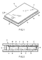
- an FED that is provided with surface-conduction electron emitting elements will be described as an example of an image display device that is manufactured by the manufacturing method and the manufacturing apparatus.
- this FED comprises a front substrate 11 and a rear substrate 12, which are each formed of a rectangular glass plate as an insulating substrate having a thickness of about 1 to 3 mm. These substrates are opposed to each other with a gap of about 1 to 2 mm between them.
- the front substrate 11 and the rear substrate 12 have their respective peripheral edge portions joined together by a sidewall 13 in the form of a rectangular frame, and constitute a flat, rectangular vacuum envelope 10 that is internally kept in a high vacuum of about 10 -4 Pa.
- a plurality of spacers 14 are provided in the vacuum envelope 10. Sheetlike or columnar spacers or the like may be used as the spacers 14.
- a phosphor screen 15 is formed as a phosphor screen on the inner surface of the front substrate 11. It has red, green, and blue stripe-shaped phosphor layers 16 and a matrix-shaped black light absorbing layer 17.
- the phosphor layers 16 may alternatively be dot-shaped.
- a large number of surface-conduction electron emitting elements 18 that individually emit electron beams are provided on the inner surface of the rear substrate 12. They serve as electron sources that excite the phosphor layers 16 of the phosphor screen 15. These electron emitting elements 18 are arranged in a plurality of columns and a plurality of rows corresponding individually to pixels. Each electron emitting element 18 includes an electron emitting portion (not shown), a pair of electrodes that apply voltage to the electron emitting portion, etc.
- a large number of wires 21 for supplying potential to the electron emitting elements 18 are arranged in a matrix on the inner surface of the rear substrate 12, and their respective end portions are drawn out of the vacuum envelope 10.
- an anode voltage is applied to the phosphor screen 15 and the metal back 20, and electron beams emitted from the electron emitting elements 18 are accelerated by the anode voltage as they hit the phosphor screen. Thereupon, the phosphor layers 16 of the phosphor screen 15 are excited to glow and display a color image.
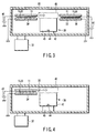
- the manufacturing apparatus is provided with a vacuum chamber 30 that is formed of a vacuum processing tank, and the vacuum chamber is connected with an exhaust pump 32 that evacuates its interior.
- a first processing electrode 34, second processing electrode 36, and getter device 38 are disposed in the vacuum chamber 30.
- the first and second processing electrodes 34 and 36 are formed each in the shape of a plate that is substantially equal in size to the substrate to be processed.
- the first and second processing electrodes 34 and 36 are arranged substantially horizontally and with a gap between them.
- the first and second processing electrodes 34 and 36 are individually connected to the ground potential.
- a getter vapor deposition position 40 is defined between the first and second processing electrodes 34 and 36, and the getter device 38 is located under the getter vapor deposition position 40.
- the getter device 38 comprises a cover 42 that opens toward the getter vapor deposition position 40, a getter material 44 provided on a bottom part in the cover, and a heating mechanism 45 for heating the getter material.
- a heating mechanism of the high-frequency heating type or resistance heating type may be used as the heating mechanism 45.
- the manufacturing apparatus is provided with a power source 46 and a substrate transportation mechanism (not shown).
- the power source 46 applies voltage to the substrate to be processed.
- the substrate transportation mechanism transports the substrate between a first electric field processing position where the substrate faces the first processing electrode 34 and a second electric field processing position where it faces the getter vapor deposition position 40 and the second processing electrode 36.
- the substrate to be processed is the front substrate 11 on which the phosphor screen 15 and the metal back 20 are formed.
- the interior of the vacuum chamber 30 is evacuated to a desired degree of vacuum by the exhaust pump 32, whereupon a vacuum atmosphere is formed in the vacuum chamber.
- the front substrate 11 is carried into the vacuum chamber 30 and set in the first electric field processing position. In this first electric field processing position, the entire surface of the front substrate 11 on the side of the metal back 20 is opposed to the first processing electrode 34 with a desired gap between them.
- the power source 46 that serves as an electric field applying section is connected electrically to the metal back 20, and voltage is applied from the power source 46 to the metal back.
- the voltage applied to the metal back 20 is set so that a positive or negative potential difference is caused between the metal back and the first processing electrode 34.
- an electric field is generated between the front substrate 11 and the first processing electrode 34, and the front substrate 11 is field-processed.
- foreign matter, such as dust having so far been left on the front substrate 11 is adsorbed and removed by the first processing electrode 34, and useless projections and the like that are formed in the process of production of the front substrate are removed.
- the front substrate 11 is transported to the getter vapor deposition position 40 without failing to keep the potential difference and the space between the first processing electrode 34 and the front substrate.
- the potential difference By maintaining the potential difference in this manner, the foreign matter adsorbed by the first processing electrode 34 or the removed projections can be held on the first processing electrode lest they adhere again to the front substrate 11.
- the front substrate 11 faces a top opening of the cover 42 of the getter device 38 with its surface on the side of the metal back 20 downward.
- the getter material 44 on the bottom part of the cover 42 is heated to be vaporized by the heating mechanism 45, whereby getter flashing is performed.
- the getter is vapor-deposited to form the getter film 22 on the metal back 20 of the front substrate 11. If the getter flashing is effected from bottom to top using the getter material 44 that is situated below the front substrate 11, dust or the like that is produced by the getter flashing can be prevented from adhering to the front substrate 11.
- the front substrate 11 is transported from the getter vapor deposition position 40 to the second electric field processing position without disconnecting the power source 46.
- the entire surface of the front substrate 11 on the side of the getter film 22 is opposed to the second processing electrode 36 with a desired gap between them.
- the front substrate 11 is moved away from the second processing electrode 36 without failing to keep the potential difference between the front substrate 11 and the second processing electrode 36 and the distance from the processing electrode 34.
- the rear substrate 12, on which the wires 21, electron emitting elements 18, etc. are formed is electric field-processed by the same aforesaid processes except the getter vapor deposition.
- the rear substrate 12 must only be electric field-processed at least once.
- the electric field-processed front and rear substrates 11 and 12 are transported to a sealing position (not shown) in a manner such that they are kept in a vacuum atmosphere without being exposed to the open air, and are then sealed together to form the vacuum envelope 10. Thereupon, the vacuum envelope of the FED is completed.
- the substrates may be sealed either in the same vacuum chamber as the vacuum chamber 30 for the aforesaid electric field processing or in another vacuum chamber that communicates with the vacuum chamber 30 in a vacuum state.
- the vacuum envelope is formed by sealing these substrates together without exposing them to the open air.
- the anode potential can be set higher, so that the FED can be obtained having high luminance and high display performance.
- the processing electrodes are provided individually before and behind the getter device 38. As in a second embodiment shown in FIG. 4, however, they may be replaced with a single processing electrode with the same result.
- a front substrate 11 is electric field-processed by a processing electrode 34, in this case, the front substrate is transported to the getter vapor deposition position 40 to be subjected to getter vapor deposition. Thereafter, the front substrate 11 is returned to the position where it faces the processing electrode 34 again, and the electric field processing is performed.
- only one processing electrode 34 may be used so that a front substrate 11 can be transported to an electric field processing position where it faces the processing electrode 34, to be field-processed, only after a getter film is formed. Also in this case, the getter film 22 that is finally exposed in a vacuum envelope and faces a rear substrate 12 is electric field-processed, whereby dust or other foreign matter adhering to the getter film and useless projections and the like that are formed in the manufacturing process can be removed. In consequence, the withstand voltage characteristics of an FED can be fully improved.
- only one processing electrode may be used so that electric field processing is performed only before the getter film is vapor-deposited. Also in this case, the withstand voltage characteristics can be improved.
- a getter device 38 that includes a getter material 44 may be located above the substrate to be processed so that the getter flashing can be effected from top to bottom. It is to be understood that the getter flashing is not limited to a vertical direction and may be performed in any other direction.
- voltage may be applied from a power source 46 to the processing electrodes 34 and 36 themselves with the substrate side kept at the ground potential as the electric field processing is performed. According to this arrangement, high voltage can be applied, so that the effect of the electric field processing can be enhanced. If a negative potential is applied to the processing electrodes 34 and 36, for example, then it can be believed that a positive potential is applied to a front substrate 11 or a rear substrate 12. Accordingly, there is a merit that effects similar to those of the foregoing embodiments can be obtained and high voltage can be applied. It is to be understood that the same effects can be also obtained if a positive potential is applied to the processing electrodes.
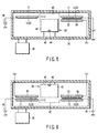
- the manufacturing apparatus is provided with a vacuum chamber 30 that is formed of a vacuum processing tank, and the vacuum chamber is connected with an exhaust pump 32 that evacuates its interior.
- a getter device 38 for forming a getter film is located in the vacuum chamber 30.
- the getter device 38 comprises a substantially box-shaped cover 42 that has an opening 37 at its lower end.
- a getter material 44 is provided on a ceiling wall in the cover 42 and faces the opening 37. Further, the getter device 38 is provided with a heating mechanism 45 for heating the getter material 44.
- a heating mechanism of the high-frequency heating type or resistance heating type may be used as the heating mechanism 45.
- the opening 37 of the cover 42 is formed having a size substantially equal to that of a substrate to be processed.
- a processing electrode 34 is provided so as to cover the opening 37 and attached to the cover 42.
- a large number of through holes for the passage of the getter are formed covering the whole processing electrode 34 and constitute an aperture portion.
- the manufacturing apparatus comprises a power source 46 and a substrate transportation mechanism (not shown).
- the power source 46 applies voltage to the substrate to be processed.
- the substrate transportation mechanism transports the substrate to a processing position, that is, electric field processing position and a getter vapor deposition position, where the substrate faces the processing electrode 34.
- the space between the getter material 44 and the processing electrode is set wider than the space between the processing electrode and the processed substrate.
- the substrate to be processed is a front substrate 11 on which a phosphor screen 15 and a metal back 20 are formed.
- the interior of the vacuum chamber 30 is evacuated to a desired degree of vacuum by the exhaust pump 32, whereupon a vacuum atmosphere is formed in the vacuum chamber.
- the front substrate 11 is carried into the vacuum chamber 30 and set in the processing position illustrated. In the processing position, the entire surface of the front substrate 11 on the side of the metal back 20 is opposed to the processing electrode 34 with a desired gap between them.
- the power source 46 that serves as an electric field applying section is connected electrically to the metal back 20, and voltage is applied from the power source 46 to the metal back.
- the processing electrode 34 is connected to the ground potential.
- the voltage applied to the metal back 20 is set so that a positive or negative potential difference is caused between the metal back and the processing electrode 34.
- an electric field is generated between the front substrate 11 and the processing electrode 34, and the front substrate 11 is electric field-processed.
- the front substrate 11 is moved to a position where it never faces the processing electrode 34 without failing to keep the potential difference between the processing electrode 34 and the front substrate 11. Accordingly, the foreign matter adsorbed by the processing electrode 34 or the removed projections can be held on the processing electrode lest the foreign matter or the removed projections fall onto and adhere again to the front substrate 11.
- the foreign matter, projections, etc. that are adsorbed by the processing electrode 34 or removed fall into the vacuum chamber 30, not onto the front substrate 11.
- the foreign matter or removed projections can be prevented from falling onto the substrate when the substrate is transported again.
- the entire surface of the front substrate 11 on the side of the metal back 20 is opposed again to the processing electrode 34 with the desired gap between them.
- the getter material 44 on the ceiling wall of the cover 42 is heated to be vaporized by the heating mechanism 45, whereby getter flashing is performed.
- a part of the getter is vapor-deposited on that region of the processing electrode 34 in which no through holes are formed, thereby forming a getter film 50.
- the remaining part of the getter passes through the through holes of the processing electrode 34, and is vapor-deposited on the metal back 20 of the front substrate 11 to form a getter film 22.
- the space between the front substrate 11 and the processing electrode 34 is set smaller than the space between the processing electrode and the getter material 44.
- the conductance between the front substrate 11 and the processing electrode 34 is smaller than the conductance between the processing electrode and the getter material 44. Therefore, gas that is released from the getter material 44 during the getter flashing first passes through the processing electrode 34 and is adsorbed by the getter film 50 on this processing electrode without reaching the front substrate 11. Thus, the getter film 22 on the front substrate 11 can never be degraded by the gas.
- the front substrate 11 is moved to a position where it never faces the processing electrode 34 without failing to keep the potential difference between the front substrate 11 and the processing electrode 34. Thereupon, the electric field processing of the front substrate 11 and the getter film formation are finished.
- the rear substrate 12 on which the wires 21, electron emitting elements 18, etc. are formed, is electric field-processed by the same aforesaid processes except the getter vapor deposition.
- the rear substrate 12 must only be electric field-processed at least once.
- the electric field-processed front and rear substrates 11 and 12 are transported to a sealing position (not shown) in a manner such that they are kept in a vacuum atmosphere without being exposed to the open air, and are then sealed together to form a vacuum envelope 10. Thereupon, the vacuum envelope of an FED is completed.
- the substrates may be sealed either in the same vacuum chamber as the vacuum chamber 30 for the aforesaid electric field processing or in another vacuum chamber that communicates with the vacuum chamber 30 in a vacuum state.
- dust or other foreign matter adhering to the front substrate 11 and the rear substrate 12 and useless projections and the like that are formed in the process of production of the front substrate and the rear substrate can be removed by electric field processing before the substrates are put into the vacuum chamber. After these substrates are put into the vacuum chamber, moreover, foreign matter, such as dust, adhering to the substrates, including dust that is produced in the getter vapor deposition process or suspended matter in the vacuum chamber, can be removed by electric field processing. Accordingly, factors that trigger generation of electric discharge can be eliminated, so that the FED with improved withstand voltage characteristics can be obtained.
- the vacuum envelope is formed without exposing these substrates to the open air.
- the anode potential can be set higher, so that the FED can be obtained having high luminance and high display performance.
- the gas adsorption properties of the getter film on the front substrate 11 can be prevented from lowering, so that a high degree of vacuum can be maintained for a prolonged time to ensure production of a long-life product.
- the electric field processing and the getter film vapor deposition can be carried out with the processed substrate held in the same position.
- the getter film is also formed on that region of the processing electrode which is not provided with the aperture portion, so that the gas that is generated during the getter flashing can be adsorbed by the getter film.
- the getter film formed on the front substrate can maintain its high gas adsorption properties without being degraded.
- the electric field processing is performed twice before and after the vapor deposition of the getter film.
- the electric field processing of the front substrate 11 may be performed only after the getter film is formed.
- the getter film 22 that is finally exposed in the vacuum envelope and faces the rear substrate 12 is electric field-processed, whereby dust or other foreign matter adhering to the getter film and useless projections and the like that are formed in the manufacturing process can be removed.
- the withstand voltage characteristics of the FED can be fully improved, and functions and effects similar to those of the foregoing embodiments can be obtained.
- the electric field processing may be performed only before the vapor deposition of the getter film. Also in this case, the withstand voltage characteristics can be improved.
- the getter flashing is effected from top to bottom using the getter material 44 that is located above the processed substrate.
- a getter material 44 may be located below a processed substrate so that getter flashing is performed from bottom to top. In this case, adhesion of dust that is produced by the getter flashing to the substrate can be reduced more securely.
- the getter flashing is not limited to a vertical direction and may be performed in any other direction.
- a processing electrode 34 is supported floating over a cover 42 by an insulating member, such as an insulator 60.
- a power source 46 is connected electrically to the processing electrode 34, and a metal back of a front substrate 11 is connected to the ground potential.
- high voltage can be applied to the processing electrode 34 itself, so that the effect of electric field processing can be enhanced.
- a negative potential is applied to the processing electrode 34, for example, then it can be believed that a positive potential is applied to a front substrate 11 or a rear substrate 12. Accordingly, there is a merit that effects similar to those of the foregoing embodiments can be obtained and high voltage can be applied. It is to be understood that the same effects can be also obtained if a positive potential is applied to the processing electrode 34.
- the processing electrodes are formed having substantially the same shape as the substrate to be processed.
- a processing electrode that is smaller in size than the substrate may be used so that the entire surface of the substrate can be electric field-processed by relatively moving the processing electrode and the substrate.
- both the front substrate and the rear substrate are electric field-processed in a vacuum atmosphere.
- an image display device with improved withstand voltage characteristics can be also obtained by electric field processing at least one of the substrates.
- This invention may be also applied to any other image display devices than FEDS.
- a manufacturing method and a manufacturing apparatus capable of manufacturing a high-performance image display device that enjoys long life, outstanding withstand voltage characteristics, and improved reliability.
Landscapes
- Engineering & Computer Science (AREA)
- Manufacturing & Machinery (AREA)
- Manufacture Of Electron Tubes, Discharge Lamp Vessels, Lead-In Wires, And The Like (AREA)
- Cathode-Ray Tubes And Fluorescent Screens For Display (AREA)
Applications Claiming Priority (5)
| Application Number | Priority Date | Filing Date | Title |
|---|---|---|---|
| JP2002227682 | 2002-08-05 | ||
| JP2002227500 | 2002-08-05 | ||
| JP2002227500 | 2002-08-05 | ||
| JP2002227682 | 2002-08-05 | ||
| PCT/JP2003/009685 WO2004013886A1 (fr) | 2002-08-05 | 2003-07-30 | Procede et dispositif pour realiser un dispositif d'affichage d'images |
Publications (1)
| Publication Number | Publication Date |
|---|---|
| EP1544890A1 true EP1544890A1 (fr) | 2005-06-22 |
Family
ID=31497633
Family Applications (1)
| Application Number | Title | Priority Date | Filing Date |
|---|---|---|---|
| EP03766665A Withdrawn EP1544890A1 (fr) | 2002-08-05 | 2003-07-30 | Procede et dispositif pour realiser un dispositif d'affichage d'images |
Country Status (6)
| Country | Link |
|---|---|
| EP (1) | EP1544890A1 (fr) |
| JP (1) | JPWO2004013886A1 (fr) |
| KR (1) | KR100730678B1 (fr) |
| CN (1) | CN1675735A (fr) |
| TW (1) | TW200405387A (fr) |
| WO (1) | WO2004013886A1 (fr) |
Families Citing this family (1)
| Publication number | Priority date | Publication date | Assignee | Title |
|---|---|---|---|---|
| CN103043921B (zh) * | 2011-10-13 | 2016-01-27 | 洛阳兰迪玻璃机器股份有限公司 | 带有吸气剂膜的真空玻璃 |
Family Cites Families (4)
| Publication number | Priority date | Publication date | Assignee | Title |
|---|---|---|---|---|
| KR100472888B1 (ko) * | 1999-01-19 | 2005-03-08 | 캐논 가부시끼가이샤 | 화상 형성 장치의 제조 방법 |
| JP2000251736A (ja) * | 1999-02-25 | 2000-09-14 | Canon Inc | 電子源の製造方法および電子源および画像形成装置および帯電処理装置 |
| JP3754883B2 (ja) * | 2000-03-23 | 2006-03-15 | キヤノン株式会社 | 画像表示装置の製造法 |
| JP2002124188A (ja) * | 2000-10-12 | 2002-04-26 | Sony Corp | 画像表示装置の製造方法 |
-
2003
- 2003-07-30 EP EP03766665A patent/EP1544890A1/fr not_active Withdrawn
- 2003-07-30 JP JP2004525801A patent/JPWO2004013886A1/ja not_active Abandoned
- 2003-07-30 CN CNA038187078A patent/CN1675735A/zh active Pending
- 2003-07-30 WO PCT/JP2003/009685 patent/WO2004013886A1/fr not_active Ceased
- 2003-07-30 KR KR1020057001956A patent/KR100730678B1/ko not_active Expired - Fee Related
- 2003-08-01 TW TW092121081A patent/TW200405387A/zh unknown
Non-Patent Citations (1)
| Title |
|---|
| See references of WO2004013886A1 * |
Also Published As
| Publication number | Publication date |
|---|---|
| KR20050026570A (ko) | 2005-03-15 |
| TW200405387A (en) | 2004-04-01 |
| WO2004013886A1 (fr) | 2004-02-12 |
| KR100730678B1 (ko) | 2007-06-21 |
| JPWO2004013886A1 (ja) | 2006-09-21 |
| CN1675735A (zh) | 2005-09-28 |
Similar Documents
| Publication | Publication Date | Title |
|---|---|---|
| KR100404557B1 (ko) | 화상 형성 장치 | |
| CN1809908A (zh) | 图像显示装置 | |
| JP3971263B2 (ja) | 画像表示装置およびその製造方法 | |
| US6169358B1 (en) | Method and apparatus for flashover control, including a high voltage spacer for parallel plate electron beam array devices and method of making thereof | |
| EP1544890A1 (fr) | Procede et dispositif pour realiser un dispositif d'affichage d'images | |
| US20050130546A1 (en) | Manufacturing method and manufacturing apparatus for image display device | |
| US7291963B2 (en) | Image display device | |
| US20060250565A1 (en) | Image display device and method of manufacturing the same | |
| US20060194502A1 (en) | Manufacturing method of image display device and manufacturing apparatus of image display device | |
| JP4005872B2 (ja) | 画像表示装置の製造方法および製造装置 | |
| JP2004071294A (ja) | 画像表示装置およびその製造方法 | |
| JP2004319180A (ja) | 画像表示装置の製造方法および製造装置 | |
| US20050082975A1 (en) | Image display device and method of manufacturing the same | |
| JP2006092797A (ja) | 基板処理方法および基板処理装置 | |
| JP2004071440A (ja) | 画像表示装置の製造方法および製造装置 | |
| JP2010067351A (ja) | 平面型表示装置及び平面型表示装置の製造方法 | |
| JP2005174677A (ja) | 画像表示装置の製造方法及び画像表示装置の製造装置 | |
| JP2006032104A (ja) | 基板処理方法および基板処理装置 | |
| JP2005197049A (ja) | 画像表示装置の製造装置及び画像表示装置の製造方法 | |
| EP1533827A1 (fr) | Dispositif d'affichage d'image et procede de fabrication | |
| JP2003109506A (ja) | 画像形成装置の製造方法、画像形成装置 | |
| CN1993798A (zh) | 平板显示装置 | |
| JP2004079358A (ja) | 画像形成装置 | |
| JP2009158374A (ja) | 基板処理装置 | |
| JP2005288384A (ja) | 基板処理方法 |
Legal Events
| Date | Code | Title | Description |
|---|---|---|---|
| PUAI | Public reference made under article 153(3) epc to a published international application that has entered the european phase |
Free format text: ORIGINAL CODE: 0009012 |
|
| 17P | Request for examination filed |
Effective date: 20050209 |
|
| AK | Designated contracting states |
Kind code of ref document: A1 Designated state(s): AT BE BG CH CY CZ DE DK EE ES FI FR GB GR HU IE IT LI LU MC NL PT RO SE SI SK TR |
|
| RBV | Designated contracting states (corrected) |
Designated state(s): DE FR GB IT NL |
|
| STAA | Information on the status of an ep patent application or granted ep patent |
Free format text: STATUS: THE APPLICATION HAS BEEN WITHDRAWN |
|
| 18W | Application withdrawn |
Effective date: 20080219 |