EP1546863B1 - Rechnerisch effiziente mathematische maschine - Google Patents
Rechnerisch effiziente mathematische maschine Download PDFInfo
- Publication number
- EP1546863B1 EP1546863B1 EP03752587A EP03752587A EP1546863B1 EP 1546863 B1 EP1546863 B1 EP 1546863B1 EP 03752587 A EP03752587 A EP 03752587A EP 03752587 A EP03752587 A EP 03752587A EP 1546863 B1 EP1546863 B1 EP 1546863B1
- Authority
- EP
- European Patent Office
- Prior art keywords
- shift register
- data
- processor
- input
- output
- Prior art date
- Legal status (The legal status is an assumption and is not a legal conclusion. Google has not performed a legal analysis and makes no representation as to the accuracy of the status listed.)
- Expired - Lifetime
Links
Images












Classifications
-
- G—PHYSICS
- G06—COMPUTING OR CALCULATING; COUNTING
- G06F—ELECTRIC DIGITAL DATA PROCESSING
- G06F7/00—Methods or arrangements for processing data by operating upon the order or content of the data handled
- G06F7/38—Methods or arrangements for performing computations using exclusively denominational number representation, e.g. using binary, ternary, decimal representation
-
- G—PHYSICS
- G06—COMPUTING OR CALCULATING; COUNTING
- G06F—ELECTRIC DIGITAL DATA PROCESSING
- G06F5/00—Methods or arrangements for data conversion without changing the order or content of the data handled
- G06F5/01—Methods or arrangements for data conversion without changing the order or content of the data handled for shifting, e.g. justifying, scaling, normalising
- G06F5/015—Methods or arrangements for data conversion without changing the order or content of the data handled for shifting, e.g. justifying, scaling, normalising having at least two separately controlled shifting levels, e.g. using shifting matrices
-
- G—PHYSICS
- G06—COMPUTING OR CALCULATING; COUNTING
- G06F—ELECTRIC DIGITAL DATA PROCESSING
- G06F17/00—Digital computing or data processing equipment or methods, specially adapted for specific functions
- G06F17/10—Complex mathematical operations
- G06F17/16—Matrix or vector computation, e.g. matrix-matrix or matrix-vector multiplication, matrix factorization
Definitions
- the present invention relates to the utilization of a mathematical engine to calculate the output of an array of complex multipliers. More specifically, the present invention is a computationally efficient mathematical engine which is accessible to perform a plurality of mathematical calculations.
- Modem wireless communication systems generally require an immense number of mathematical calculations to perform signal processing. Such calculations are generally performed by processors and application specific integrated circuits (ASICs).
- ASICs application specific integrated circuits
- Standard ASIC design for a receiver requires the implementation and calculation of many algorithms, which often require many parallel multiplications in order to complete the calculations during the allotted time. These algorithms typically consist of many matrix-to-matrix and matrix-to-vector multiplications and many discrete Fourier transform (DFT) and fast Fourier transform (FFT) calculations. Because multipliers take up a lot of room on an ASIC, it is desirable to devise a solution which is capable of applying the same multipliers across the several algorithms.
- DFT discrete Fourier transform
- FFT fast Fourier transform
- Certain common calculations may be used to support a variety of current wireless technologies such as WCDMA, WTT, CDMA2000, 802.1X, TDSCDMA, FDD, TDD, and also other future system architectures not presently contemplated.
- One such type of calculation which is commonly performed is the dot product multiplication.
- Performing a dot-product calculation is a standard function as an operation between two matrixes. For example, dot product calculations are required for performing channel estimation and data estimation.
- such calculations may include calculation of the prime factor fast Fourier transform (FFT), multiplication of a matrix by another matrix, multiplication of a matrix by its complex conjugate transpose, and a multiplication of a matrix by a vector.
- FFT prime factor fast Fourier transform
- FIG. 1 shows a device having a processor with four multiplier units in parallel, thus having a capacity of processing eight values at a time. There are eight registers with each four values (Fi and XFi), and one input is selected from each register by respective MUXes 22-28. These inputs are presented to the multiplier units and the products added.
- the present invention includes a memory having a parallel output used to store one or more values which are selectively output in a parallel output of logically adjacent values.
- the memory is addressed so as to provide portions of the vector, referred to as a fold, in a logical sequence which permits completion of a mathematical execution on the full vector.
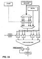
- Figure 1 is a general block diagram of the mathematical engine of the present invention.
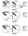
- Figures 2A - 2C show multiplication of the System Response Matrix (A H ) with its complex conjugate transpose (A) to calculate the Autocorrelation Matrix (A H A).
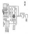
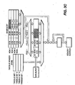
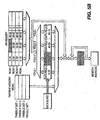
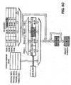
- Figures 3A - 3G show the mathematical engine of Figure 1 performing the calculations required for the A H A function.
- Figures 4A - 4D show multiplication of the A H matrix with the received signal vector (r).
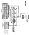
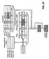
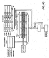
- Figures 5A - 5I show the mathematical engine of Figure 1 performing the calculations required for the A H r function.
- Figures 6A - 6D show the mathematical engine of Figure 1 performing the calculations required for a DFT.
- Figures 7A - 7C illustrate selective use of the input sources.
- the present invention is a single mathematical engine for processing a plurality of separate and distinct algorithms.
- the mathematical engine is capable of utilizing the same hardware for all of the algorithms. Because multipliers require significant space on the ASIC, the present invention reduces the amount of required space for the ASIC.
- the mathematical engine of the present invention is also very efficient in performing required calculations by using the hardware a higher percentage of the time. The efficiency of the mathematical engine is dependent on the sizes of the input matrixes and the number of processing elements.
- the mathematical engine has at least two inputs and one output.
- the inputs include a serial input and a parallel input, where the parallel input is as wide as the number of processing elements.
- the number of processing elements may be optimized to be an entire vector, a piece of a vector, or a vector of a matrix.
- the parallel and serial inputs can both be loaded into a shift register, or another type of serial access register, for different types of operations.
- the parallel output shift register is a memory which has a parallel output and which permits rapid output of the data stored.
- the parallel output of the shift register is multiplexed such that logically adjacent values, whose width is determined by the number of processing elements, can perform the function of a serial access register, can perform the function of a parallel output shift register having a selectable output, or can provide access to a secondary parallel input.
- the primary parallel input and the multiplexed parallel output of the shift register and secondary parallel input act as inputs to complex multipliers and an adder tree, which increases the efficiency of the calculations performed by the mathematical engine. This permits data to be moved into the registers as quickly as possible for each of the performed operations, and also permits reorganization of the data for internal steps of the operation to be performed efficiently.
- the parallel output shift register outputs data from logically adjacent data values, so that the output is used to store a value which is selectively output in parallel to a computational section.
- the parallel output shift register is addressed so as to provide portions of the vector in a sequence which permits completion of a mathematical execution on the full vector. As a result, almost every clock results in a calculation, instead of multiple steps to prepare the data for the operation.
- the parallel output shift register is a parallel output n-fold shift register, meaning that its memory store is n times the data width of the computational section (i.e. the number of the processing elements).
- the adder tree feeds an accumulator, which enables many different matrix-to-matrix and matrix-to-vector multiplications and enables efficient calculations such as A H A and A H r.
- the dot product calculations performed by the mathematical engine include, but are not limited to, a plurality of different types of multiplications required for channel estimation and data estimation such as: the prime factor FFT; the multiplication of a matrix by another matrix, multiplication of a matrix by its complex conjugate transpose, and a multiplication of a matrix by a vector.
- the mathematical engine 30 includes a Primary Parallel Data Input Source (PPDIS) 31, a demultiplexer 32, an n-fold shift register 33, a Serial Data Input Source (SDIS) 34, a multiplexer 35 and a Secondary Parallel Data Input Source (SPDIS) 36. Also included is a complex multiplier processing element (PE) array 40, consisting of a plurality of array elements.(41-44 shown), a complex adder tree 55 and an complex accumulator 56.
- the complex accumulator 56 includes an initial condition input multiplexer 58, a summer 57, and a summer output register 59.
- the summer output register 59 provides an accumulated output.
- the PE array 40 provides parallel complex multiplication functions, including dot product outputs.
- the output of the PPDIS 31 contains Q locations.
- the SDIS 34 provides the shift register 33 with a complex received chip sequence. This output from the SDIS 34 is used to serially load the shift register 33.
- the shift register 33 has n-folds, where each fold has Q locations with each location containing a complex value. Additionally it can load any fold with values from the Q locations from the PPDIS 31, or shift in X locations of zeros every clock.
- the multiplexer 35 receives an output from the shift register 33 and a complex Q location value from PPDIS 36.
- the output from the multiplexer 35 is provided to the complex multiplier array 40 which is used to provide corresponding inputs to the complex adder tree 55.
- the complex adder tree 55 is a Q input complex adder tree.
- the adder tree 55 provides its output to the accumulator 56.
- the accumulator 56 is provided with an initial condition at the summer 57, which is supplied through multiplexer 58.
- the result of the output of summer 57 is stored in the output register 59.
- the mathematical engine 30 of the present invention shown in Figure 1 is able to perform several different types of calculations, thereby obviating the need for separate processors and, as a result greatly reducing the amount of ASIC real estate required for such mathematical calculations.
- Three different applications of the preferred embodiment in a WTDD communication system are described hereinafter, but are not limited to: 1) generation of the Autocorrelation Matrix (A H A); 2) Whitened Matched Filtering (A H r); and 3) Channel Estimation implemented via the Steiner Algorithm.
- a H A Autocorrelation Matrix
- a H r Whitened Matched Filtering
- Steiner Algorithm Channel Estimation implemented via the Steiner Algorithm
- a H A function is one of the most complex functions calculated with a mathematical engine because it is calculated from a partially stored matrix and the same partially stored matrix accessed in a different manner with only a partially calculated result.
- the order of the operations is not based on a logical progression of matrixes, but rather how the matrixes fit through the existing functions of the mathematical engine.
- Figure 2A is a simple field matrix representation of the A" , A and A H A matrixes. Only the A H row block is stored in memory, so the entire A H and A matrixes are represented as addressing functions on the stored row block with the ability to access the data with the imaginary portion of the data inverted to use the data as in the A matrix. The resulting A H A matrix is stored compressed, as if it was constructed from the A H and A matrixes.
- the first step is to copy the contents of the A H Memory into the shift register 33 where it can also be manipulated to represent the second and third row blocks as they are seen only by the window of data used in the calculations.
- Figures 3A , 3B and 3C show the first three clock cycles which demonstrate the loading of the first A H row into the shift register.
- Figure 2B shows the first row of the A H matrix times the first column of the A matrix resulting in the first value of the A H A matrix.
- the calculation is done one fold at a time, (or 3 folds done over 3 clocks).
- Each of the fold segments are multiplied and accumulated in the accumulation register 59, (shown in Figure 1 ) until the entire row is done, at which time the result is stored external to the mathematical engine.
- the A H matrix is represented by the values in the shift register while the A matrix values are represented in the A H memory with an inverse function on the imaginary values, which is performed, by taking their conjugate in the complex multiplier array 40 ( shown in Figure 1 ).
- Figure 3D shows the multiplication of the first fold of the first row of the A H matrix with that of the first fold of the first column of the A matrix. The result of this multiplication is stored in the accumulation register 59.
- Figure 3E shows the multiplication of the second fold of the first row of the A H matrix with that of the second fold of the first column of the A matrix. The accumulated result of this multiplication is added to the previous accumulated value and is stored in the accumulation register 59.
- Figure 3F shows the multiplication of the third fold of the first row of the A H matrix with that of the third fold of the first column of the A matrix. The accumulated result of this multiplication is added to the previous accumulated value and is stored in the accumulation register 59.
- the value stored in the accumulation registers 59 represents the first location of the A H A matrix and is stored externally for further processing.
- This multiplication takes 3 clocks, one for each fold, but only the first clock is represented in Figure 3G , which shows the multiplication of the first fold of the first row of the A H matrix with that of the first fold of the second valid column of the A matrix.
- the result of this multiplication is stored in the accumulation register 59. This process proceeds for 3 clocks until the accumulated result is stored externally for further processing.
- the A H r function as performed by the mathematical engine of Figure 1 will be described with reference to Figures 4A -4D and Figures 5A - 5I .
- the A H r function is the multiplication of the entire A H matrix with the received vector (r).
- the A H matrix is not entirely stored, only a smaller portion called the A H row block is actually stored; all the other values in the A H matrix are actually repeated A H row block, or zeros. Accordingly, A H can be stored as a complex addressing scheme of the A H row block.
- Figure 4A is a diagram representing the A H r matrix multiplication.
- the A H row block is repeated throughout the A H matrix with all the rest zeros. Of the rows of the A H row block, two of the four rows have been invalidated by prior processing.
- the first step in calculating A H r function is to preload the entire shift register 33 of the mathematical engine with the r vector values.
- the shift register 33 (shown in Figure 1 ), is loaded serially by the SDIS 34.
- the A H matrix is provided at the PPDIS 31.
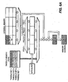
- Figure 5A shows the first fold of the first A H row being multiplied by the first fold of the r vector and the result being stored into the accumulation register 59.
- Figure 5B shows the second fold of the first A H row being multiplied by the second fold of the r vector and the result being added to the result currently in the accumulator register 59.
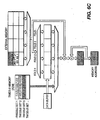
- Figure 5C shows the third fold of the first A H row being multiplied by the third fold of the r vector and the result being added to the result currently in the accumulator register 59. The resulting accumulation is now stored as the first A H r calculation point.
- the next step is to calculate the next valid row of the A H row block with the currently calculated symbol.
- the r vector can remain the same but a different row of A H is accessed in the A H memory.
- Figures 5D , 5E and 5F showing the multiplication accumulation of all three folds.
- Figure 5D shows the first fold of the third A H row being multiplied by the first fold of the r vector and the result being stored into the accumulation register 59.
- Figure 5E shows the second fold of the third A H row being multiplied by the second fold of the r vector and the result being added to the result currently in the accumulator register 59.
- Figures 5F shows the third fold of the third A H row being multiplied by the third fold of the r vector and the result being added to the result currently in the accumulator register 59. The resulting as the second A H r calculation point.
- the next step is to start the calculations of the second A H row block with the r vector. This involves multiplying each of the valid A H second row sub block rows with the r vector. The portion of the r vector that is multiplied by the A H sub block is different, since the next row is shifted in 16 values from the last. In Figure 4D the portions involved in the calculation are highlighted.
- the r vector Since the A H row block stored is not moving, the r vector has to be shifted to re-align the portion of the r vector that is multiplied by the row in the new A H row block. This is done by using the shift register 33, shifting in 16 new values over 16 clocks, and dropping off the first values of the r vector.
- the first two clocks of this process are shown in Figures 5G and 5H , the rest are inferred. After that, the same process as used for the first A H row block is started, so the first clock of this repeated operation is shown to be compared with the first clock of the first A H row block.
- Figure 5G shows one value of the r vector being shifted into the right side of the shift register while the first value put into the shift register is lost.
- Figure 5H shows a second value of the r vector being shifted into the shift register while the second value put into the register is lost.
- Figure 5I shows the first A H row being multiplied by the first fold of the newly shifted r vector and the result being stored into the accumulation register 59 just as in the first calculation of the first A H r row block. This process continues for every fold of every valid A H row block row for every one of the A H row blocks.
- the Steiner algorithm as performed by the mathematical engine of Figure 1 will be described with reference to Figures 6A -6D .
- the figures show the process of using the mathematical engine to do a 3pt DFT for a 456 pt Steiner.
- Figures 6A - 6C show the calculation of the first DFT, each figure showing a different clock.
- the first three addresses of the DFT were already loaded into the memory serially so they can all be accessed at once in a parallel manner, through the PPDIS 31, (in Figure 1 ).
- the Twiddle Factors used for the DFT are inputted through the SPDIS 36, (in Figure 1 ).
- the first DFT inputs at addresses 0, 152, and 304 are multiplied by one of the three twiddle factor sets unique to that point of the DFT.
- the results of these three calculations are external to the mathematical engine in Figure 1 .
- Figure 6D shows how the first point of the next DFT is calculated with the first twiddle factor set and the other two sets will follow in the following clocks.
- a 64-point DFT is done in a slightly different manner where the multiplication of each DFT set by the twiddle set takes four consecutive clocks that are accumulated together before storage.
- the PPDIS provides the system response matrix (A H ). Additionally, the serial input is used to provide the data fields of the received vector (r) during the A H r operation.
- the system response matrix A H is multiplied by the data fields of the received vector r for a timeslot.
- the data field is loaded into the shift register while the system response matrix is provided to the primary parallel input.
- the PPDIS provides the FFT input data set and the SPDIS provides the FFT twiddle factors.
- the FFT operations in an m-point FFT, the appropriate m-points of the data set are provided by the PPDIS to the complex multiplier array, while the appropriate FFT Twiddle factors are provided by the SPDIS.
Landscapes
- Engineering & Computer Science (AREA)
- Physics & Mathematics (AREA)
- Theoretical Computer Science (AREA)
- General Physics & Mathematics (AREA)
- Mathematical Physics (AREA)
- Computational Mathematics (AREA)
- Mathematical Analysis (AREA)
- Mathematical Optimization (AREA)
- Pure & Applied Mathematics (AREA)
- General Engineering & Computer Science (AREA)
- Data Mining & Analysis (AREA)
- Computing Systems (AREA)
- Databases & Information Systems (AREA)
- Software Systems (AREA)
- Algebra (AREA)
- Complex Calculations (AREA)
- Ultra Sonic Daignosis Equipment (AREA)
- Apparatus For Radiation Diagnosis (AREA)
- Pharmaceuticals Containing Other Organic And Inorganic Compounds (AREA)
- Control Of Electric Motors In General (AREA)
- Image Processing (AREA)
- Measuring Fluid Pressure (AREA)
- Electrical Control Of Air Or Fuel Supplied To Internal-Combustion Engine (AREA)
Claims (18)
- Recheneinheit, die aufweist:einen Prozessor mit einer Mehrzahl von arithmetischen Logikeinheits-, ALU-Schaltungen (40), die konfiguriert sind, um Daten parallel zu verarbeiten und verarbeitete Datenausgaben bereitzustellen, wobei die Anzahl von ALU-Schaltungen die Kapazität des Prozessors definiert, und mit einem Addiererbaum, der konfiguriert ist, um die verarbeiteten Datenausgaben von den ALU-Schaltungen zu addieren;ein Schieberegister (33) mit einem parallelen Ausgang und einer höheren Kapazität als der Kapazität des Prozessors; undeine Einrichtung zum Steuern des Schieberegisters, um selektiv Daten von dem parallelen Ausgang auszugeben, um der Kapazität des Prozessors zu entsprechen.
- Recheneinheit nach Anspruch 1, die ferner einen Multiplexer (35) aufweist, der konfiguriert ist, um selektiv Ausgangsdaten von dem Schieberegister zu empfangen und selektiv derartige Daten von dem Schieberegister als Eingabe an die ALU-Schaltungen (40) bereitzustellen.
- Recheneinheit nach Anspruch 1 oder 2, wobei das Schieberegister sowohl serielle als auch parallele Eingänge hat, die ferner durch eine Freigabeschaltung gekennzeichnet sind, die konfiguriert ist, um selektiv die seriellen und parallelen Eingänge des Schieberegisters freizugeben.
- Recheneinheit nach Anspruch 1, 2 oder 3, die ferner durch einen Eingangsspeicher (31) gekennzeichnet ist, der mit dem Schieberegister (33) und den Prozessor-ALU-Schaltungen (40) verbunden ist, und eine Auswahlschaltung zum selektiven Freigeben des Eingangs zu dem Schieberegister (33) und den Prozessor-ALU-Schaltungen (40) von dem Eingangsspeicher (33) basierend auf der Art der durchgeführten Berechnung.
- Recheneinheit nach Anspruch 4, die ferner durch einen sekundären Eingangsspeicher (36) gekennzeichnet ist,
wobei die Auswahlschaltung aufgebaut ist, um den Eingang von dem sekundären Eingangsspeicher (36) zu dem Prozessor basierend auf der Art der durchgeführten Berechnung selektiv freizugeben. - Recheneinheit nach Anspruch 1, 2, 3, 4 oder 5, wobei das Schieberegister (33) als ein auswählbarer Speicher konfiguriert ist, um Eingangsdaten von wenigstens einer Eingangsquelle zu empfangen, und die Einrichtung zum selektiven Steuern des Schieberegisters konfiguriert ist, um eine wählbare Ausgabe über mehrere Fächer auszugeben, wobei jedes Fach eine Kapazität hat, die der Kapazität des Prozessors entspricht, und wenigstens eine andere Position innerhalb des auswählbaren Speichers aufweist.
- Recheneinheit nach Anspruch 1, 2, 3, 4, 5 oder 6, die ferner eine Akkumulationsschaltung zum Empfangen und selektiven Akkumulieren jeder Ausgabe von dem Addiererbaum basierend auf der Art der durchgeführten Berechnung aufweist.
- Recheneinheit nach Anspruch 1, die ferner gekennzeichnet ist durch:einen Speicher (31) zum Empfangen von Eingangsdaten für die komplexe Auflösung;eine Ablage (36) zum Ablegen eines Operationsfaktors für die komplexe Funktion;einen Multiplexer (35), der konfiguriert ist, um selektiv über den Speicher oder die Ablage Eingaben von dem Schieberegister (33) zu empfangen;wobei die Prozessor-ALU-Schaltungen (40) als eine Verarbeitungsmatrixschaltung zum Verarbeiten von Daten von ausgewählten Bitstellen, die von dem Speicher gespeichert werden, und von dem Multiplexer ausgegebenen Daten konfiguriert sind; und
wobei eine Akkumulationsschaltung eine Ausgabe von dem Addiererbaum empfängt und eine akkumulierte komplexe Ausgabe bereitstellt. - Recheneinheit nach Anspruch 8, wobei die Ablage (36) konfiguriert ist, um einen Twiddle-Faktor als den Operationsfaktor bereitzustellen, um diskrete Fouriertransformationen (DFTs) durchzuführen, wobei der Multiplexer seine Eingabe von der Ablage (36) empfängt, wenn der Twiddle-Faktor verwendet wird.
- Recheneinheit nach Anspruch 1, 2, 3, 4, 5, 6, 7, 8 oder 9, wobei der Prozessor konfiguriert ist, um Daten zu verarbeiten, die sowohl reale als auch imaginäre Komponenten enthalten.
- Kommunikationsvorrichtung, welche die Berechnungseinheit nach einem der Ansprüche 1 - 10 enthält so konfiguriert ist, um die Verarbeitung von drahtlosen Kommunikationssignalen zu erleichtern.
- Verfahren zur Verarbeitung von Daten, das aufweist:Bereitstellen eines Prozessors, der einen Addiererbaum (55) und eine Mehrzahl von arithmetischen Logikeinheits-, ALU-Schaltungen (40) hat, wobei die Anzahl von ALU-Schaltungen die Kapazität des Prozessors definiert;Bereitstellen eines Schieberegisters (33), das einen parallelen Ausgang und eine höhere Kapazität als die Kapazität des Prozessors hat;Empfangen der Daten, die verarbeitet werden sollen, in dem Schieberegister;Steuern des Schieberegisters, um selektiv Daten auszugeben, um der Kapazität des Prozessors zu entsprechen;Verwenden der ALU-Schaltungen des Prozessors, um von dem Schieberegister ausgegebene Daten parallel zu verarbeiten und verarbeitete Datenausgaben bereitzustellen; undVerwenden des Addiererbaums, um die verarbeiteten Datenausgaben von den ALU-Schaltungen zu addieren.
- Verfahren nach Anspruch 12, das ferner die Verwendung eines Multiplexers (35) aufweist, um selektiv Ausgangsdaten von dem Schieberegister zu empfangen und selektiv derartige Daten von dem Schieberegister an die ALU-Schaltungen (40) bereitzustellen.
- Verfahren nach Anspruch 12 oder 13, wobei das Schieberegister sowohl serielle als auch parallele Eingänge hat, das ferner durch selektives Freigeben der seriellen und parallelen Eingänge des Schieberegisters basierend auf der Art der durchzuführenden Datenverarbeitungsberechnungen gekennzeichnet ist.
- Verfahren nach Anspruch 12, 13 oder 14, wobei ein Eingangsspeicher (31) mit dem Schieberegister (33) und den Prozessor-ALU-Schaltungen (40) verbunden ist, das ferner dadurch gekennzeichnet ist, daß es den Eingang zu dem Schieberegister (33) und den Prozessor-ALU-Schaltungen (40) von dem Eingangsspeicher (33) basierend auf der Art der durchgeführten Berechnung selektiv freigibt.
- Verfahren nach Anspruch 15, das ferner dadurch gekennzeichnet ist, daß der Eingang von einem sekundären Eingangsspeicher (36) zu dem Prozessor basierend auf der Art der durchgeführten Berechnung selektiv freigegeben wird.
- Verfahren nach Anspruch 12, 13, 14, 15 oder 16,
wobei die Daten, die verarbeitet werden, Daten sind, die sowohl reale als auch imaginäre Komponenten enthalten. - Verfahren nach Anspruch 12, 13, 14, 15, 16 oder 17, das in einer Kommunikationsvorrichtung durchgeführt wird, um die Verarbeitung drahtloser Kommunikationssignale zu erleichtern.
Priority Applications (1)
| Application Number | Priority Date | Filing Date | Title |
|---|---|---|---|
| EP09171791A EP2146278A1 (de) | 2002-09-24 | 2003-09-24 | Recheneffiziente Mathematikmaschine |
Applications Claiming Priority (3)
| Application Number | Priority Date | Filing Date | Title |
|---|---|---|---|
| US41316402P | 2002-09-24 | 2002-09-24 | |
| US413164P | 2002-09-24 | ||
| PCT/US2003/030089 WO2004029793A1 (en) | 2002-09-24 | 2003-09-24 | Computationally efficient mathematical engine |
Related Child Applications (1)
| Application Number | Title | Priority Date | Filing Date |
|---|---|---|---|
| EP09171791A Division EP2146278A1 (de) | 2002-09-24 | 2003-09-24 | Recheneffiziente Mathematikmaschine |
Publications (3)
| Publication Number | Publication Date |
|---|---|
| EP1546863A1 EP1546863A1 (de) | 2005-06-29 |
| EP1546863A4 EP1546863A4 (de) | 2006-04-19 |
| EP1546863B1 true EP1546863B1 (de) | 2010-01-20 |
Family
ID=32043214
Family Applications (2)
| Application Number | Title | Priority Date | Filing Date |
|---|---|---|---|
| EP03752587A Expired - Lifetime EP1546863B1 (de) | 2002-09-24 | 2003-09-24 | Rechnerisch effiziente mathematische maschine |
| EP09171791A Withdrawn EP2146278A1 (de) | 2002-09-24 | 2003-09-24 | Recheneffiziente Mathematikmaschine |
Family Applications After (1)
| Application Number | Title | Priority Date | Filing Date |
|---|---|---|---|
| EP09171791A Withdrawn EP2146278A1 (de) | 2002-09-24 | 2003-09-24 | Recheneffiziente Mathematikmaschine |
Country Status (11)
| Country | Link |
|---|---|
| US (2) | US7430577B2 (de) |
| EP (2) | EP1546863B1 (de) |
| JP (1) | JP4263693B2 (de) |
| KR (3) | KR20090046939A (de) |
| CN (1) | CN1685309B (de) |
| AT (1) | ATE456086T1 (de) |
| AU (1) | AU2003270874A1 (de) |
| CA (1) | CA2499929A1 (de) |
| DE (1) | DE60331088D1 (de) |
| NO (1) | NO20051806L (de) |
| WO (1) | WO2004029793A1 (de) |
Families Citing this family (17)
| Publication number | Priority date | Publication date | Assignee | Title |
|---|---|---|---|---|
| US20060149804A1 (en) * | 2004-11-30 | 2006-07-06 | International Business Machines Corporation | Multiply-sum dot product instruction with mask and splat |
| KR20070075946A (ko) * | 2006-01-17 | 2007-07-24 | 장영범 | 저전력 고속 푸리에 변환 방법 및 장치와, 이를 이용한통신 단말기 |
| US20080071851A1 (en) * | 2006-09-20 | 2008-03-20 | Ronen Zohar | Instruction and logic for performing a dot-product operation |
| US9495724B2 (en) * | 2006-10-31 | 2016-11-15 | International Business Machines Corporation | Single precision vector permute immediate with “word” vector write mask |
| US8332452B2 (en) * | 2006-10-31 | 2012-12-11 | International Business Machines Corporation | Single precision vector dot product with “word” vector write mask |
| US8175853B2 (en) * | 2008-03-28 | 2012-05-08 | International Business Machines Corporation | Systems and methods for a combined matrix-vector and matrix transpose vector multiply for a block-sparse matrix |
| US8626815B1 (en) * | 2008-07-14 | 2014-01-07 | Altera Corporation | Configuring a programmable integrated circuit device to perform matrix multiplication |
| CN101847093B (zh) * | 2010-04-28 | 2013-09-04 | 中国科学院自动化研究所 | 具有可重构低功耗数据交织网络的数字信号处理器 |
| CN102707931A (zh) * | 2012-05-09 | 2012-10-03 | 刘大可 | 一种基于并行数据通道的数字信号处理器 |
| US9503747B2 (en) * | 2015-01-28 | 2016-11-22 | Intel Corporation | Threshold filtering of compressed domain data using steering vector |
| WO2017131711A1 (en) | 2016-01-28 | 2017-08-03 | Hewlett Packard Enterprise Development Lp | Memristor crossbar array for performing a fourier transformation |
| US10089110B2 (en) * | 2016-07-02 | 2018-10-02 | Intel Corporation | Systems, apparatuses, and methods for cumulative product |
| CN108475188A (zh) * | 2017-07-31 | 2018-08-31 | 深圳市大疆创新科技有限公司 | 数据处理方法和设备 |
| US10754649B2 (en) | 2018-07-24 | 2020-08-25 | Apple Inc. | Computation engine that operates in matrix and vector modes |
| US12174911B2 (en) | 2020-12-23 | 2024-12-24 | Intel Corporation | Apparatus and method for complex matrix multiplication |
| US12216734B2 (en) * | 2020-12-23 | 2025-02-04 | Intel Corporation | Apparatus and method for conjugate transpose and multiply |
| US12153899B2 (en) | 2020-12-23 | 2024-11-26 | Intel Corporation | Apparatus and method for complex matrix transpose and multiply |
Family Cites Families (25)
| Publication number | Priority date | Publication date | Assignee | Title |
|---|---|---|---|---|
| US3535694A (en) | 1968-01-15 | 1970-10-20 | Ibm | Information transposing system |
| JPS58207177A (ja) | 1982-05-28 | 1983-12-02 | Nec Corp | 演算装置 |
| US4811210A (en) * | 1985-11-27 | 1989-03-07 | Texas Instruments Incorporated | A plurality of optical crossbar switches and exchange switches for parallel processor computer |
| JPH0734228B2 (ja) | 1987-02-23 | 1995-04-12 | 株式会社東芝 | 複合類似度法によるパタ−ン認識装置 |
| JPH07113886B2 (ja) * | 1987-05-11 | 1995-12-06 | 株式会社日立製作所 | 演算回路 |
| US5268856A (en) * | 1988-06-06 | 1993-12-07 | Applied Intelligent Systems, Inc. | Bit serial floating point parallel processing system and method |
| US5050119A (en) * | 1989-10-06 | 1991-09-17 | North American Philips Corporation | Optimized sparse transversal filter |
| US5179531A (en) * | 1990-04-27 | 1993-01-12 | Pioneer Electronic Corporation | Accelerated digital signal processor |
| US5301340A (en) * | 1990-10-31 | 1994-04-05 | International Business Machines Corporation | IC chips including ALUs and identical register files whereby a number of ALUs directly and concurrently write results to every register file per cycle |
| US5487089A (en) * | 1992-02-17 | 1996-01-23 | Matsushita Electric Industrial Co., Ltd. | Nyquist filter for digital modulation |
| JP3413940B2 (ja) | 1994-03-29 | 2003-06-09 | ソニー株式会社 | 演算回路 |
| US5909572A (en) | 1996-12-02 | 1999-06-01 | Compaq Computer Corp. | System and method for conditionally moving an operand from a source register to a destination register |
| DE69839316T2 (de) * | 1997-01-20 | 2009-04-16 | Matsushita Electric Industrial Co., Ltd., Kadoma-shi | Digitale Kamera mit auswechselbaren Anzeigevorrichtungen |
| US6401194B1 (en) * | 1997-01-28 | 2002-06-04 | Samsung Electronics Co., Ltd. | Execution unit for processing a data stream independently and in parallel |
| US5974435A (en) * | 1997-08-28 | 1999-10-26 | Malleable Technologies, Inc. | Reconfigurable arithmetic datapath |
| US6317770B1 (en) * | 1997-08-30 | 2001-11-13 | Lg Electronics Inc. | High speed digital signal processor |
| JP3765171B2 (ja) * | 1997-10-07 | 2006-04-12 | ヤマハ株式会社 | 音声符号化復号方式 |
| DE69927075T2 (de) * | 1998-02-04 | 2006-06-14 | Texas Instruments Inc | Rekonfigurierbarer Koprozessor mit mehreren Multiplizier-Akkumulier-Einheiten |
| US6334176B1 (en) | 1998-04-17 | 2001-12-25 | Motorola, Inc. | Method and apparatus for generating an alignment control vector |
| JP3287305B2 (ja) | 1998-04-23 | 2002-06-04 | 日本電気株式会社 | 積和演算装置 |
| US6839728B2 (en) | 1998-10-09 | 2005-01-04 | Pts Corporation | Efficient complex multiplication and fast fourier transform (FFT) implementation on the manarray architecture |
| US6366937B1 (en) | 1999-03-11 | 2002-04-02 | Hitachi America Ltd. | System and method for performing a fast fourier transform using a matrix-vector multiply instruction |
| US6526430B1 (en) | 1999-10-04 | 2003-02-25 | Texas Instruments Incorporated | Reconfigurable SIMD coprocessor architecture for sum of absolute differences and symmetric filtering (scalable MAC engine for image processing) |
| JP3338043B2 (ja) | 2000-11-02 | 2002-10-28 | 株式会社ソニー・コンピュータエンタテインメント | 並列演算装置、エンタテインメント装置、演算処理方法、コンピュータプログラム、半導体デバイス |
| US6922716B2 (en) * | 2001-07-13 | 2005-07-26 | Motorola, Inc. | Method and apparatus for vector processing |
-
2003
- 2003-09-24 EP EP03752587A patent/EP1546863B1/de not_active Expired - Lifetime
- 2003-09-24 CA CA002499929A patent/CA2499929A1/en not_active Abandoned
- 2003-09-24 WO PCT/US2003/030089 patent/WO2004029793A1/en not_active Ceased
- 2003-09-24 JP JP2004539858A patent/JP4263693B2/ja not_active Expired - Fee Related
- 2003-09-24 KR KR1020097005290A patent/KR20090046939A/ko not_active Withdrawn
- 2003-09-24 EP EP09171791A patent/EP2146278A1/de not_active Withdrawn
- 2003-09-24 KR KR1020057004974A patent/KR100708270B1/ko not_active Expired - Fee Related
- 2003-09-24 US US10/670,062 patent/US7430577B2/en not_active Expired - Fee Related
- 2003-09-24 KR KR1020057017502A patent/KR20050099641A/ko not_active Withdrawn
- 2003-09-24 CN CN038226995A patent/CN1685309B/zh not_active Expired - Fee Related
- 2003-09-24 AU AU2003270874A patent/AU2003270874A1/en not_active Abandoned
- 2003-09-24 AT AT03752587T patent/ATE456086T1/de not_active IP Right Cessation
- 2003-09-24 DE DE60331088T patent/DE60331088D1/de not_active Expired - Lifetime
-
2005
- 2005-04-13 NO NO20051806A patent/NO20051806L/no not_active Application Discontinuation
-
2008
- 2008-08-20 US US12/194,975 patent/US8112467B2/en not_active Expired - Fee Related
Also Published As
| Publication number | Publication date |
|---|---|
| US20080307205A1 (en) | 2008-12-11 |
| US20040230632A1 (en) | 2004-11-18 |
| EP1546863A1 (de) | 2005-06-29 |
| WO2004029793A1 (en) | 2004-04-08 |
| CA2499929A1 (en) | 2004-04-08 |
| US8112467B2 (en) | 2012-02-07 |
| NO20051806L (no) | 2005-06-08 |
| KR20050099641A (ko) | 2005-10-14 |
| KR100708270B1 (ko) | 2007-04-17 |
| JP2006500684A (ja) | 2006-01-05 |
| DE60331088D1 (de) | 2010-03-11 |
| CN1685309A (zh) | 2005-10-19 |
| KR20090046939A (ko) | 2009-05-11 |
| EP1546863A4 (de) | 2006-04-19 |
| CN1685309B (zh) | 2010-08-11 |
| AU2003270874A1 (en) | 2004-04-19 |
| NO20051806D0 (no) | 2005-04-13 |
| EP2146278A1 (de) | 2010-01-20 |
| US7430577B2 (en) | 2008-09-30 |
| JP4263693B2 (ja) | 2009-05-13 |
| ATE456086T1 (de) | 2010-02-15 |
| KR20050061477A (ko) | 2005-06-22 |
Similar Documents
| Publication | Publication Date | Title |
|---|---|---|
| US8112467B2 (en) | Computationally efficient mathematical engine | |
| US7870176B2 (en) | Method of and apparatus for implementing fast orthogonal transforms of variable size | |
| US4138730A (en) | High speed FFT processor | |
| US4117541A (en) | Configurable parallel arithmetic structure for recursive digital filtering | |
| US4601006A (en) | Architecture for two dimensional fast fourier transform | |
| US4199660A (en) | FDM/TDM Transmultiplexer | |
| EP2017743A2 (de) | Effizientes Hochgeschwindigkeitshardwaremodul zur Matrizenmultiplikation | |
| US7415584B2 (en) | Interleaving input sequences to memory | |
| EP0575033B1 (de) | Architektur zur Erzeugung einer kovarianten Matrize | |
| US7720897B2 (en) | Optimized discrete fourier transform method and apparatus using prime factor algorithm | |
| US20050114420A1 (en) | Pipelined FFT processor with memory address interleaving | |
| EP1444798A1 (de) | Array-verarbeitung für lineare systemlösungen | |
| US6189021B1 (en) | Method for forming two-dimensional discrete cosine transform and its inverse involving a reduced number of multiplication operations | |
| KR101162649B1 (ko) | 가변적 크기의 고속 직교 변환을 구현하기 위한 방법 및장치 | |
| US20010039557A1 (en) | Digital signal processor | |
| US6658441B1 (en) | Apparatus and method for recursive parallel and pipelined fast fourier transform | |
| EP1076296A2 (de) | Datenspeichervorrichtung für schnelle Fourier-Transformation | |
| US6092093A (en) | Multiplexer device for frequency bands | |
| CA2451167A1 (en) | Pipelined fft processor with memory address interleaving | |
| JP2001160736A (ja) | デジタルフィルタ回路 | |
| Hsiao et al. | A high-throughput, low power architecture and its VLSI implementation for DFT/IDFT computation | |
| WO2005052798A1 (en) | Interleaving memory |
Legal Events
| Date | Code | Title | Description |
|---|---|---|---|
| PUAI | Public reference made under article 153(3) epc to a published international application that has entered the european phase |
Free format text: ORIGINAL CODE: 0009012 |
|
| 17P | Request for examination filed |
Effective date: 20050421 |
|
| AK | Designated contracting states |
Kind code of ref document: A1 Designated state(s): AT BE BG CH CY CZ DE DK EE ES FI FR GB GR HU IE IT LI LU MC NL PT RO SE SI SK TR |
|
| RIC1 | Information provided on ipc code assigned before grant |
Ipc: 7G 06F 5/01 B Ipc: 7G 06F 7/38 A Ipc: 7G 06F 7/52 B Ipc: 7G 06F 17/16 B |
|
| A4 | Supplementary search report drawn up and despatched |
Effective date: 20060306 |
|
| RIC1 | Information provided on ipc code assigned before grant |
Ipc: G06F 7/38 20060101AFI20040413BHEP Ipc: G06F 17/14 20060101ALI20060228BHEP Ipc: G06F 5/01 20060101ALI20060228BHEP Ipc: G06F 7/52 20060101ALI20060228BHEP Ipc: G06F 17/16 20060101ALI20060228BHEP |
|
| RIN1 | Information on inventor provided before grant (corrected) |
Inventor name: TIMMERMAN, CHAYIL, S. Inventor name: SUPPLEE, STEPHAN, SHANE Inventor name: BUCHERT, RYAN, S. |
|
| 17Q | First examination report despatched |
Effective date: 20060913 |
|
| 17Q | First examination report despatched |
Effective date: 20060913 |
|
| GRAP | Despatch of communication of intention to grant a patent |
Free format text: ORIGINAL CODE: EPIDOSNIGR1 |
|
| GRAS | Grant fee paid |
Free format text: ORIGINAL CODE: EPIDOSNIGR3 |
|
| GRAL | Information related to payment of fee for publishing/printing deleted |
Free format text: ORIGINAL CODE: EPIDOSDIGR3 |
|
| GRAS | Grant fee paid |
Free format text: ORIGINAL CODE: EPIDOSNIGR3 |
|
| RAP1 | Party data changed (applicant data changed or rights of an application transferred) |
Owner name: INTERDIGITAL TECHNOLOGY CORPORATION |
|
| GRAA | (expected) grant |
Free format text: ORIGINAL CODE: 0009210 |
|
| AK | Designated contracting states |
Kind code of ref document: B1 Designated state(s): AT BE BG CH CY CZ DE DK EE ES FI FR GB GR HU IE IT LI LU MC NL PT RO SE SI SK TR |
|
| REG | Reference to a national code |
Ref country code: GB Ref legal event code: FG4D |
|
| REG | Reference to a national code |
Ref country code: CH Ref legal event code: EP |
|
| REG | Reference to a national code |
Ref country code: IE Ref legal event code: FG4D |
|
| REF | Corresponds to: |
Ref document number: 60331088 Country of ref document: DE Date of ref document: 20100311 Kind code of ref document: P |
|
| REG | Reference to a national code |
Ref country code: NL Ref legal event code: T3 |
|
| PG25 | Lapsed in a contracting state [announced via postgrant information from national office to epo] |
Ref country code: AT Free format text: LAPSE BECAUSE OF FAILURE TO SUBMIT A TRANSLATION OF THE DESCRIPTION OR TO PAY THE FEE WITHIN THE PRESCRIBED TIME-LIMIT Effective date: 20100120 |
|
| PG25 | Lapsed in a contracting state [announced via postgrant information from national office to epo] |
Ref country code: ES Free format text: LAPSE BECAUSE OF FAILURE TO SUBMIT A TRANSLATION OF THE DESCRIPTION OR TO PAY THE FEE WITHIN THE PRESCRIBED TIME-LIMIT Effective date: 20100501 Ref country code: PT Free format text: LAPSE BECAUSE OF FAILURE TO SUBMIT A TRANSLATION OF THE DESCRIPTION OR TO PAY THE FEE WITHIN THE PRESCRIBED TIME-LIMIT Effective date: 20100520 |
|
| PG25 | Lapsed in a contracting state [announced via postgrant information from national office to epo] |
Ref country code: FI Free format text: LAPSE BECAUSE OF FAILURE TO SUBMIT A TRANSLATION OF THE DESCRIPTION OR TO PAY THE FEE WITHIN THE PRESCRIBED TIME-LIMIT Effective date: 20100120 Ref country code: SI Free format text: LAPSE BECAUSE OF FAILURE TO SUBMIT A TRANSLATION OF THE DESCRIPTION OR TO PAY THE FEE WITHIN THE PRESCRIBED TIME-LIMIT Effective date: 20100120 |
|
| PG25 | Lapsed in a contracting state [announced via postgrant information from national office to epo] |
Ref country code: CY Free format text: LAPSE BECAUSE OF FAILURE TO SUBMIT A TRANSLATION OF THE DESCRIPTION OR TO PAY THE FEE WITHIN THE PRESCRIBED TIME-LIMIT Effective date: 20100120 Ref country code: BE Free format text: LAPSE BECAUSE OF FAILURE TO SUBMIT A TRANSLATION OF THE DESCRIPTION OR TO PAY THE FEE WITHIN THE PRESCRIBED TIME-LIMIT Effective date: 20100120 Ref country code: GR Free format text: LAPSE BECAUSE OF FAILURE TO SUBMIT A TRANSLATION OF THE DESCRIPTION OR TO PAY THE FEE WITHIN THE PRESCRIBED TIME-LIMIT Effective date: 20100421 Ref country code: EE Free format text: LAPSE BECAUSE OF FAILURE TO SUBMIT A TRANSLATION OF THE DESCRIPTION OR TO PAY THE FEE WITHIN THE PRESCRIBED TIME-LIMIT Effective date: 20100120 Ref country code: RO Free format text: LAPSE BECAUSE OF FAILURE TO SUBMIT A TRANSLATION OF THE DESCRIPTION OR TO PAY THE FEE WITHIN THE PRESCRIBED TIME-LIMIT Effective date: 20100120 Ref country code: SE Free format text: LAPSE BECAUSE OF FAILURE TO SUBMIT A TRANSLATION OF THE DESCRIPTION OR TO PAY THE FEE WITHIN THE PRESCRIBED TIME-LIMIT Effective date: 20100120 |
|
| PLBE | No opposition filed within time limit |
Free format text: ORIGINAL CODE: 0009261 |
|
| STAA | Information on the status of an ep patent application or granted ep patent |
Free format text: STATUS: NO OPPOSITION FILED WITHIN TIME LIMIT |
|
| PG25 | Lapsed in a contracting state [announced via postgrant information from national office to epo] |
Ref country code: BG Free format text: LAPSE BECAUSE OF FAILURE TO SUBMIT A TRANSLATION OF THE DESCRIPTION OR TO PAY THE FEE WITHIN THE PRESCRIBED TIME-LIMIT Effective date: 20100420 Ref country code: CZ Free format text: LAPSE BECAUSE OF FAILURE TO SUBMIT A TRANSLATION OF THE DESCRIPTION OR TO PAY THE FEE WITHIN THE PRESCRIBED TIME-LIMIT Effective date: 20100120 Ref country code: SK Free format text: LAPSE BECAUSE OF FAILURE TO SUBMIT A TRANSLATION OF THE DESCRIPTION OR TO PAY THE FEE WITHIN THE PRESCRIBED TIME-LIMIT Effective date: 20100120 |
|
| 26N | No opposition filed |
Effective date: 20101021 |
|
| PG25 | Lapsed in a contracting state [announced via postgrant information from national office to epo] |
Ref country code: DK Free format text: LAPSE BECAUSE OF FAILURE TO SUBMIT A TRANSLATION OF THE DESCRIPTION OR TO PAY THE FEE WITHIN THE PRESCRIBED TIME-LIMIT Effective date: 20100120 |
|
| PG25 | Lapsed in a contracting state [announced via postgrant information from national office to epo] |
Ref country code: IT Free format text: LAPSE BECAUSE OF FAILURE TO SUBMIT A TRANSLATION OF THE DESCRIPTION OR TO PAY THE FEE WITHIN THE PRESCRIBED TIME-LIMIT Effective date: 20100120 |
|
| PG25 | Lapsed in a contracting state [announced via postgrant information from national office to epo] |
Ref country code: MC Free format text: LAPSE BECAUSE OF NON-PAYMENT OF DUE FEES Effective date: 20100930 |
|
| REG | Reference to a national code |
Ref country code: CH Ref legal event code: PL |
|
| PG25 | Lapsed in a contracting state [announced via postgrant information from national office to epo] |
Ref country code: CH Free format text: LAPSE BECAUSE OF NON-PAYMENT OF DUE FEES Effective date: 20100930 Ref country code: LI Free format text: LAPSE BECAUSE OF NON-PAYMENT OF DUE FEES Effective date: 20100930 Ref country code: IE Free format text: LAPSE BECAUSE OF NON-PAYMENT OF DUE FEES Effective date: 20100924 |
|
| PG25 | Lapsed in a contracting state [announced via postgrant information from national office to epo] |
Ref country code: HU Free format text: LAPSE BECAUSE OF FAILURE TO SUBMIT A TRANSLATION OF THE DESCRIPTION OR TO PAY THE FEE WITHIN THE PRESCRIBED TIME-LIMIT Effective date: 20100721 Ref country code: LU Free format text: LAPSE BECAUSE OF NON-PAYMENT OF DUE FEES Effective date: 20100924 |
|
| PG25 | Lapsed in a contracting state [announced via postgrant information from national office to epo] |
Ref country code: TR Free format text: LAPSE BECAUSE OF FAILURE TO SUBMIT A TRANSLATION OF THE DESCRIPTION OR TO PAY THE FEE WITHIN THE PRESCRIBED TIME-LIMIT Effective date: 20100120 |
|
| PGFP | Annual fee paid to national office [announced via postgrant information from national office to epo] |
Ref country code: NL Payment date: 20130910 Year of fee payment: 11 Ref country code: DE Payment date: 20130918 Year of fee payment: 11 |
|
| PGFP | Annual fee paid to national office [announced via postgrant information from national office to epo] |
Ref country code: GB Payment date: 20130918 Year of fee payment: 11 Ref country code: FR Payment date: 20130910 Year of fee payment: 11 |
|
| REG | Reference to a national code |
Ref country code: DE Ref legal event code: R119 Ref document number: 60331088 Country of ref document: DE |
|
| GBPC | Gb: european patent ceased through non-payment of renewal fee |
Effective date: 20140924 |
|
| REG | Reference to a national code |
Ref country code: FR Ref legal event code: ST Effective date: 20150529 |
|
| PG25 | Lapsed in a contracting state [announced via postgrant information from national office to epo] |
Ref country code: NL Free format text: LAPSE BECAUSE OF NON-PAYMENT OF DUE FEES Effective date: 20150401 |
|
| PG25 | Lapsed in a contracting state [announced via postgrant information from national office to epo] |
Ref country code: GB Free format text: LAPSE BECAUSE OF NON-PAYMENT OF DUE FEES Effective date: 20140924 Ref country code: DE Free format text: LAPSE BECAUSE OF NON-PAYMENT OF DUE FEES Effective date: 20150401 |
|
| PG25 | Lapsed in a contracting state [announced via postgrant information from national office to epo] |
Ref country code: FR Free format text: LAPSE BECAUSE OF NON-PAYMENT OF DUE FEES Effective date: 20140930 |