EP1550928A1 - Procede de codage de blocs et circuit de codage/decodage de blocs - Google Patents
Procede de codage de blocs et circuit de codage/decodage de blocs Download PDFInfo
- Publication number
- EP1550928A1 EP1550928A1 EP03751378A EP03751378A EP1550928A1 EP 1550928 A1 EP1550928 A1 EP 1550928A1 EP 03751378 A EP03751378 A EP 03751378A EP 03751378 A EP03751378 A EP 03751378A EP 1550928 A1 EP1550928 A1 EP 1550928A1
- Authority
- EP
- European Patent Office
- Prior art keywords
- data
- encryption
- key data
- circuit
- decryption
- Prior art date
- Legal status (The legal status is an assumption and is not a legal conclusion. Google has not performed a legal analysis and makes no representation as to the accuracy of the status listed.)
- Withdrawn
Links
Images


Classifications
-
- H—ELECTRICITY
- H04—ELECTRIC COMMUNICATION TECHNIQUE
- H04L—TRANSMISSION OF DIGITAL INFORMATION, e.g. TELEGRAPHIC COMMUNICATION
- H04L9/00—Cryptographic mechanisms or cryptographic arrangements for secret or secure communications; Network security protocols
- H04L9/06—Cryptographic mechanisms or cryptographic arrangements for secret or secure communications; Network security protocols the encryption apparatus using shift registers or memories for block-wise or stream coding, e.g. DES systems or RC4; Hash functions; Pseudorandom sequence generators
- H04L9/0618—Block ciphers, i.e. encrypting groups of characters of a plain text message using fixed encryption transformation
- H04L9/0631—Substitution permutation network [SPN], i.e. cipher composed of a number of stages or rounds each involving linear and nonlinear transformations, e.g. AES algorithms
-
- H—ELECTRICITY
- H04—ELECTRIC COMMUNICATION TECHNIQUE
- H04L—TRANSMISSION OF DIGITAL INFORMATION, e.g. TELEGRAPHIC COMMUNICATION
- H04L9/00—Cryptographic mechanisms or cryptographic arrangements for secret or secure communications; Network security protocols
- H04L9/06—Cryptographic mechanisms or cryptographic arrangements for secret or secure communications; Network security protocols the encryption apparatus using shift registers or memories for block-wise or stream coding, e.g. DES systems or RC4; Hash functions; Pseudorandom sequence generators
-
- G—PHYSICS
- G06—COMPUTING OR CALCULATING; COUNTING
- G06C—DIGITAL COMPUTERS IN WHICH ALL THE COMPUTATION IS EFFECTED MECHANICALLY
- G06C1/00—Computing aids in which the computing members form at least part of the displayed result and are manipulated directly by hand, e.g. abacuses or pocket adding devices
-
- G—PHYSICS
- G09—EDUCATION; CRYPTOGRAPHY; DISPLAY; ADVERTISING; SEALS
- G09C—CIPHERING OR DECIPHERING APPARATUS FOR CRYPTOGRAPHIC OR OTHER PURPOSES INVOLVING THE NEED FOR SECRECY
- G09C1/00—Apparatus or methods whereby a given sequence of signs, e.g. an intelligible text, is transformed into an unintelligible sequence of signs by transposing the signs or groups of signs or by replacing them by others according to a predetermined system
-
- H—ELECTRICITY
- H04—ELECTRIC COMMUNICATION TECHNIQUE
- H04L—TRANSMISSION OF DIGITAL INFORMATION, e.g. TELEGRAPHIC COMMUNICATION
- H04L9/00—Cryptographic mechanisms or cryptographic arrangements for secret or secure communications; Network security protocols
- H04L9/30—Public key, i.e. encryption algorithm being computationally infeasible to invert or user's encryption keys not requiring secrecy
-
- H—ELECTRICITY
- H04—ELECTRIC COMMUNICATION TECHNIQUE
- H04L—TRANSMISSION OF DIGITAL INFORMATION, e.g. TELEGRAPHIC COMMUNICATION
- H04L2209/00—Additional information or applications relating to cryptographic mechanisms or cryptographic arrangements for secret or secure communication H04L9/00
- H04L2209/12—Details relating to cryptographic hardware or logic circuitry
-
- H—ELECTRICITY
- H04—ELECTRIC COMMUNICATION TECHNIQUE
- H04L—TRANSMISSION OF DIGITAL INFORMATION, e.g. TELEGRAPHIC COMMUNICATION
- H04L2209/00—Additional information or applications relating to cryptographic mechanisms or cryptographic arrangements for secret or secure communication H04L9/00
- H04L2209/24—Key scheduling, i.e. generating round keys or sub-keys for block encryption
Definitions
- the present invention relates to a block cipher method and a block encryption/decryption circuit.
- a block cipher circuit using the Advanced Encryption Standard is one of the cipher circuits for encrypting plaintext data.
- Such an AES block cipher circuit divides data to be encrypted into, for example, 128-bit blocks and encrypts them one by one with round key data.
- the round key data is generated from key data for the encryption by a key scheduling process (refer to, for example, "AES gaisetu”, [online], dated June 11, 2002, IWATA Lab., Department of Electrical & Computer Engineering, Nagoya Institute of Technology, [searched on Oct. 8, 2002], at http://mars.elcom.nitech.ac.jp/security/aes.html).
- the key scheduling process generally requires about twice the processing time for the encryption or decryption. Accordingly, the key scheduling for each block or for each task in multitasking, shown in step 2 or 4, causes considerable overhead, thus decreasing the total throughput of the encryption or decryption.
- the present invention provides, for example, a block cipher method including the steps of: generating first round key data depending on key data for decryption, storing the first round key data at a first location of a memory, generating second round key data depending on key data for encryption, storing the second round key data at a second location of the memory, decrypting blocks of input ciphertext data one by one into plaintext data with the first round key data, and encrypting the blocks of plaintext data one by one with the second round key data.
- reference numeral 10 denotes the overall structure of a block encryption/decryption circuit according to the present invention and reference numeral 20 denotes a host computer that connects the block encryption/decryption circuit 10.
- the block encryption/decryption circuit 10 can execute fast re-encryption of ciphertext data.
- a memory 23 of the host computer 20 stores ciphertext data to be re-encrypted, key data for decrypting the ciphertext data into plaintext data, and key data for re-encrypting the plaintext data into encrypted data.
- One block of the original ciphertext data is, for example, 128 bits and the length of the key data for the encryption or decryption is also 128 bits.
- the block encryption/decryption circuit 10 has two modes. In the first mode, round key data for decryption is generated from the key data for the decryption and is stored in the memory, while round key data for encryption is generated from the key data for the encryption and also is stored in the memory. In the second mode, a decryption of the ciphertext data block into a plaintext data block and a re-encryption of the plaintext data block are alternately carried out for the series of blocks by using the round key data stored in the memory in the first mode.
- the block encryption/decryption circuit 10 includes an encrypting/decrypting circuit 11 and a key scheduling circuit 12.
- the encrypting/decrypting circuit 11 decrypts a block of the ciphertext data into plaintext data with the round key data for decryption, and encrypts a block of the plaintext data into encrypted data with the round key data for encryption.
- the key scheduling circuit 12 generates the round key data for decryption from the key data for decryption and generates the round key data for encryption from the key data for encryption.
- the encrypting/decrypting circuit 11 and the key scheduling circuit 12 are connected to an internal bus 19 of the block encryption/decryption circuit 10.
- the internal bus 19 is connected to the host computer 20.
- a register 15 is connected to the internal bus 19.
- the register 15 has a mode flag MFLG.
- the mode flag MFLG is set by the host computer 20 and supplied to the encrypting/decrypting circuit 11 and the key scheduling circuit 12 to control the circuits as follows:
- the block encryption/decryption circuit 10 has a bank memory 13 and a register 14.
- the bank memory 13 has a pair of banks #0 and #1, which store the round key data for the encryption and the decryption generated by the key scheduling circuit 12, respectively.
- the register 15 has a switching flag BNKF, which is set by the host computer 20 and supplied to the bank memory 13 as a control signal to switch the banks.
- the bank memory 13 is controlled as follows:
- the block encryption/decryption circuit 10 has a memory control circuit 16, which controls read/write of the round key data from/to the bank memory 13 and its addresses.
- the output of the bank memory 13 is temporarily stored in the register 14, and then supplied to the encrypting/decrypting circuit 11 as the round key data.
- the switching flag BNKF of the register 15 is supplied to the encrypting/decrypting circuit 11 for the following control:
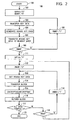
- the block encryption/decryption circuit 10 carries out the re-encryption of ciphertext data stored in the host computer 20 in the flow shown in, for example, a flow chart 100 in Fig. 2. The process will be described hereinafter. 1.2 Re-encryption process of the block encryption/decryption circuit 10
- the re-encryption of the ciphertext data starts at step 101 in the flow chart 100.
- the flags MFLG and BNKF in the register 15 are then set to level "0" by the host computer 20. Accordingly, the mode flag MFLG enables the key scheduling circuit 12 and disables the encrypting/decrypting circuit 11, while the switching flag BNKF enables the bank #0 and disables the bank #1.
- the host computer 20 sets the mode flag MFLG to level "0" so that, as shown in step 103, the host computer 20 transfers the decryption key data, which is one of the key data items stored in the memory 23, to the key scheduling circuit 12.
- the key scheduling circuit 12 generates round key data from the key data transferred in step 103.
- BNKF "0"; hence, round key data for the decryption is generated.
- step 105 the round key data generated in step 104 is transferred to the bank memory 13 by the memory control circuit 16.
- step 106 the level of the switching flag BNKF is checked.
- BNKF "0"; hence the process flow proceeds from step 106 to step 107, where the switching flag BNKF in the register 15 is set to level "1" by the host computer 20. The process flow then returns to step 103.
- the key data for encryption which is the other key data stored in the memory 23, is transferred to the key scheduling circuit 12 (step 103).
- Round key data for the encryption is generated from the key data (step 104).
- the round key data is written into the bank #1 of the bank memory 13 (step 105).
- BNKF "1" in step 106; hence, the process flow proceeds from step 106 to step 111.
- the round key data for the decryption and the round key data for the re-encryption are stored in the bank #0 and the bank #1 of the bank memory 13, respectively.
- step 111 the mode flag MFLG of the register 15 is set to level "1" so that the mode flag MFLG disables the key scheduling circuit 12 and enables the encrypting/decrypting circuit 11.
- step 112 the switching flag BNKF is set to level "0" so that the switching flag BNKF enables the bank #0, disables the bank #1, and enables the encrypting/decrypting circuit 11 to carry out the decryption.
- step 113 the round key data stored in the enabled bank #0 or #1, on this occasion, in the bank #0, is supplied to the encrypting/decrypting circuit 11 via the register 14.
- step 116 the block of the plaintext data decrypted in step 115 is returned to the memory 23 of the host computer 20.
- step 117 it is determined whether the process of all the data in the memory 23 is completed. At this point, it is not completed, then the process flow proceeds to step 118.
- steps 113 to 116 are repeated again.
- BNKF "1"
- the bank #1 of the bank memory 13 is enabled and the round key data for the decryption is retrieved and supplied to the encrypting/decrypting circuit 11 (step 113).
- the second block of the ciphertext data in the memory 23 is decrypted into plaintext data and is re-encrypted into ciphertext data in steps 111 to 119. Also, the decryption into the plaintext data and re-encryption into the ciphertext data are carried out by using the round key data for the decryption and encryption stored in banks #0 and #1 of the bank memory 13 in steps 101 to 105.
- step 117 After the entire ciphertext data in the memory 23 is re-encrypted, the process flow proceeds from step 117 to step 121 and the flow chart 100 completes.
- the ciphertext data in the memory 23 is re-encrypted.
- the re-encryption requires the round key data for the decryption and re-encryption. These round key data are prepared in the banks #0 and #1 of the bank memory 13 in advance, thereby only one key scheduling is sufficient for each of the decryption and re-encryption. Consequently, the time required for re-encrypting the ciphertext data is significantly decreased, thus increasing the total throughput.
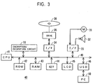
- Fig. 3 shows an embodiment according to the present invention applied to a CD-R/RW recording and playback unit.
- reference numeral 31 denotes a signal source of audio signal, such as a microphone 31, and reference numeral 32 denotes a destination of the audio signal, such as a speaker 32.
- a system bus 49 of a microcomputer 40 which will be described below, via an audio interface circuit 33.
- a disk drive unit 35 is connected to the system bus 49 via a disk interface circuit 34.
- a disk 36 such as a Compact Disc Recordable (CD-R) or a Compact Disc Rewritable (CD-RW), is mounted in the disk drive unit 35.
- CD-R Compact Disc Recordable
- CD-RW Compact Disc Rewritable
- the microcomputer 40 corresponds to the host computer 20 in the embodiments 1.1 and 1.2, and constitutes a system control circuit that controls the overall operation of the recording and playback unit.
- the microcomputer 40 includes a central processing unit (CPU) 41, a read only memory (ROM) 42, in which various types of programs and data are written, and a random access memory (RAM) 43 for a working area, which are all connected to the system bus 49.
- the block encryption/decryption circuit 10 which is described in the embodiments 1.1 and 1.2, is connected to the system bus 49 via the internal bus 19. A part of the address area of the RAM 43 is used as the memory 23.
- USB Universal Serial Bus
- audio signals are supplied from the microphone 31 to the audio interface circuit 33 and are A/D (Analog-to-digital) converted to digital audio data.
- the digital audio data are supplied to the disk interface circuit 34 via the system bus 49, are encoded for error correction, and are EFM (Eight to Fourteen Modulation) modulated for recording. Then, the encoded and modulated signals are supplied to the disk drive unit 35 and are recorded onto the disk 36.
- Signals from the disk 36 are played back by the disk drive unit 35.
- the played-back signals are supplied to the disk interface circuit 34, in which the original audio data are retrieved through processes complementary to the recording processes, that is, EFM demodulation and a decoding process for error correction.
- the digital audio data are then supplied to the audio interface circuit 33 via the system bus 49 and are D/A (Digital to Analog) converted to analog audio signals, which are supplied to the speaker 32.
- the audio signals are supplied from the microphone 31 to the audio interface circuit 33, in which the audio signals are A/D converted to digital audio data.
- the digital audio data is buffered and then supplied to the block encryption/decryption circuit 10.
- the digital audio data in the RAM 43 are block encrypted for every 2 K (1024) bytes into ciphertext data by the block encryption/decryption circuit 10, as described in the embodiments 1.1 to 1.2.
- the ciphertext data in the RAM 43 are supplied to the disk interface circuit 34, encoded for error correction, and EFM modulated for recording, and are then supplied to the disk drive unit 35 to be recorded to the disk 36.
- the audio signals recorded on the disk 36 are decrypted and played back
- the audio signals are played back from the disk 36 by the disk drive unit 35.
- the played-back signals are supplied to the disk interface circuit 34, in which the signals are decoded into the original ciphertext data.
- the ciphertext data are buffered in the RAM 43, and then, for example, every 2 K bytes of the data are supplied to the block encryption/decryption circuit 10 and block decrypted into the original digital audio data, as described in the embodiments 1.1 to 1.2.
- the decrypted digital audio data are supplied from the RAM 43 to the audio interface circuit 33, and D/A converted into the original analog audio signals, which are supplied to the speaker 32.
- the playback signals from the disk 36 are decoded into the original ciphertext data by the disk interface circuit 34.
- the ciphertext data are sequentially written into the RAM 43.
- some amount of the ciphertext data for example, the ciphertext data in one sector of the disk 36, are written into the RAM 43, the process shown in the flow chart 100 is carried out so that the ciphertext data in the RAM 43 are re-encrypted and then supplied to the personal computer 50 via the USB interface circuit 46. Subsequently, the above-described process is repeated each time the ciphertext data in a sector of the disk 36 are played back.
- the encrypted audio signals recorded on the disk 36 are re-encrypted to output to the personal computer 50.
- re-encryption overhead is eliminated so that the process can be carried out in real time during the playback of the disk 36.
- the switching flag BNKF should be set to level "0" or level "1" in accordance with the executed task and steps 103 to 105 should be executed, and then steps 111 and 113 to 117 should be executed. Subsequently, the process flow returns from step 117 to step 113. These steps carry out the processes corresponding to either encryption or decryption. Similarly, in the cases of three or more tasks, a bank of the bank memory 13 should be switched to the bank corresponding to each task, and then steps 103 to 105, 111, and steps 113 to 117 should be executed.
- the ciphertext data or the decrypted data has one piece of key data. It may have a plurality of pieces of key data.
- the encrypting/decrypting circuit 11 may be a generic block cipher circuit.
- the key scheduling circuit 12 may be incorporated in the encrypting/decrypting circuit 11.
- the round key data for the encryption or decryption are stored in banks of a bank memory.
- the key scheduling is carried out only once. Compared to the process requiring key scheduling for every block of plaintext data or ciphertext data, the overhead is eliminated, thus considerably decreasing the required time for the encryption or decryption and increasing the total throughput.
Landscapes
- Engineering & Computer Science (AREA)
- Computer Security & Cryptography (AREA)
- Computer Networks & Wireless Communication (AREA)
- Signal Processing (AREA)
- Theoretical Computer Science (AREA)
- Physics & Mathematics (AREA)
- Computing Systems (AREA)
- General Physics & Mathematics (AREA)
- Mathematical Physics (AREA)
- Computer Hardware Design (AREA)
- Storage Device Security (AREA)
Applications Claiming Priority (3)
| Application Number | Priority Date | Filing Date | Title |
|---|---|---|---|
| JP2002295808 | 2002-10-09 | ||
| JP2002295808A JP2004133087A (ja) | 2002-10-09 | 2002-10-09 | ブロック暗号方法およびブロック暗号回路 |
| PCT/JP2003/012877 WO2004034171A1 (fr) | 2002-10-09 | 2003-10-08 | Procede de codage de blocs et circuit de codage/decodage de blocs |
Publications (1)
| Publication Number | Publication Date |
|---|---|
| EP1550928A1 true EP1550928A1 (fr) | 2005-07-06 |
Family
ID=32089223
Family Applications (1)
| Application Number | Title | Priority Date | Filing Date |
|---|---|---|---|
| EP03751378A Withdrawn EP1550928A1 (fr) | 2002-10-09 | 2003-10-08 | Procede de codage de blocs et circuit de codage/decodage de blocs |
Country Status (6)
| Country | Link |
|---|---|
| US (1) | US7386124B2 (fr) |
| EP (1) | EP1550928A1 (fr) |
| JP (1) | JP2004133087A (fr) |
| KR (1) | KR20050069927A (fr) |
| CN (1) | CN100524150C (fr) |
| WO (1) | WO2004034171A1 (fr) |
Families Citing this family (9)
| Publication number | Priority date | Publication date | Assignee | Title |
|---|---|---|---|---|
| JP4752113B2 (ja) * | 2001-01-16 | 2011-08-17 | ソニー株式会社 | 電子機器及び信号伝送方法 |
| KR100949538B1 (ko) * | 2008-09-09 | 2010-03-25 | 한국전자통신연구원 | Aes 라인달 알고리즘을 이용하는 암호화 및 복호화 장치와 그 방법 |
| US8233620B2 (en) * | 2009-02-27 | 2012-07-31 | Inside Secure | Key recovery mechanism for cryptographic systems |
| JP5353828B2 (ja) * | 2010-06-14 | 2013-11-27 | 富士通セミコンダクター株式会社 | プロセッサ及びプロセッサシステム |
| CN102063179A (zh) * | 2011-01-13 | 2011-05-18 | 浙江大学 | 一种生成轮密钥的分组密码算法的低功耗装置及方法 |
| KR101516574B1 (ko) | 2014-02-21 | 2015-05-04 | 한국전자통신연구원 | 형태보존 암호화를 위한 가변길이 블록암호 장치 및 방법 |
| US10341090B2 (en) * | 2014-10-14 | 2019-07-02 | Sony Corporation | Cipher processing apparatus and cipher processing method |
| CN110311771B (zh) * | 2018-03-20 | 2022-07-22 | 北京小米松果电子有限公司 | Sm4加解密方法及电路 |
| CN118944871A (zh) * | 2024-07-24 | 2024-11-12 | 西安电子科技大学 | 一次一密的存储密钥更新方法、系统、设备和可读存储介质 |
Family Cites Families (15)
| Publication number | Priority date | Publication date | Assignee | Title |
|---|---|---|---|---|
| DE3824328C1 (fr) * | 1988-07-18 | 1989-12-21 | Kone-Anlagenbau Gmbh, 8900 Augsburg, De | |
| DE3910444C3 (de) * | 1989-03-31 | 1998-10-22 | Wifag Maschf | Automatische Anlage zum Einbringen von Papierrollen in die Rollenständer einer Rollenrotationsdruckmaschine |
| JPH06149153A (ja) | 1992-11-02 | 1994-05-27 | Nippon Telegr & Teleph Corp <Ntt> | 汎用高速暗号装置 |
| EP0715241B1 (fr) * | 1994-10-27 | 2004-01-14 | Mitsubishi Corporation | Appareil pour système de gestion de droits d'auteur de données |
| JP3502200B2 (ja) * | 1995-08-30 | 2004-03-02 | 株式会社日立製作所 | 暗号通信システム |
| US5726283A (en) * | 1997-01-03 | 1998-03-10 | Far Eastern Textile, Ltd. | Conductive polyester sheet |
| DE19847160A1 (de) * | 1998-10-13 | 2000-04-20 | Hauni Maschinenbau Ag | Bobinenwechsler |
| JP3679936B2 (ja) * | 1998-11-27 | 2005-08-03 | 東芝ソリューション株式会社 | 暗復号装置及び記憶媒体 |
| US7003107B2 (en) * | 2000-05-23 | 2006-02-21 | Mainstream Encryption | Hybrid stream cipher |
| JP4153653B2 (ja) * | 2000-10-31 | 2008-09-24 | 株式会社東芝 | マイクロプロセッサおよびデータ保護方法 |
| US20020124177A1 (en) * | 2001-01-17 | 2002-09-05 | Harper Travis Kelly | Methods for encrypting and decrypting electronically stored medical records and other digital documents for secure storage, retrieval and sharing of such documents |
| US6937727B2 (en) * | 2001-06-08 | 2005-08-30 | Corrent Corporation | Circuit and method for implementing the advanced encryption standard block cipher algorithm in a system having a plurality of channels |
| US7203310B2 (en) * | 2001-12-04 | 2007-04-10 | Microsoft Corporation | Methods and systems for cryptographically protecting secure content |
| US7006628B2 (en) * | 2002-01-04 | 2006-02-28 | Avaya Technology Corp. | Efficient packet encryption method |
| US7221763B2 (en) * | 2002-04-24 | 2007-05-22 | Silicon Storage Technology, Inc. | High throughput AES architecture |
-
2002
- 2002-10-09 JP JP2002295808A patent/JP2004133087A/ja active Pending
-
2003
- 2003-10-08 WO PCT/JP2003/012877 patent/WO2004034171A1/fr not_active Ceased
- 2003-10-08 CN CNB2003801000282A patent/CN100524150C/zh not_active Expired - Fee Related
- 2003-10-08 US US10/496,306 patent/US7386124B2/en not_active Expired - Fee Related
- 2003-10-08 EP EP03751378A patent/EP1550928A1/fr not_active Withdrawn
- 2003-10-08 KR KR1020047008752A patent/KR20050069927A/ko not_active Ceased
Non-Patent Citations (1)
| Title |
|---|
| See references of WO2004034171A1 * |
Also Published As
| Publication number | Publication date |
|---|---|
| US20050232414A1 (en) | 2005-10-20 |
| WO2004034171A1 (fr) | 2004-04-22 |
| CN1685296A (zh) | 2005-10-19 |
| CN100524150C (zh) | 2009-08-05 |
| US7386124B2 (en) | 2008-06-10 |
| KR20050069927A (ko) | 2005-07-05 |
| JP2004133087A (ja) | 2004-04-30 |
Similar Documents
| Publication | Publication Date | Title |
|---|---|---|
| US5513262A (en) | Device for enciphering and deciphering, by means of the DES algorithm, data to be written to be read from a hard disk | |
| CN100514471C (zh) | 用器件访问移动介质上的加密内容的方法和系统 | |
| KR100683342B1 (ko) | 디지털 데이터 기록장치, 디지털 데이터 메모리장치, 및제한정보를 포함하는 관리정보를 각 관리정보 송신/수신세션 내의 상이한 키를 이용하여 변환하는 디지털 데이터이용장치 | |
| US7529366B2 (en) | Block encoding/decoding method, circuit, and device | |
| WO2010055658A1 (fr) | Appareil de décodage de contenu, procédé de décodage de contenu et circuit intégré | |
| JP2004226969A (ja) | 暗号システム及び多様なモードを支援する方法 | |
| KR101117588B1 (ko) | 암호화 표시정보를 갖는 기록매체 | |
| JP2010185982A (ja) | 暗号化装置、復号化装置及び記憶装置 | |
| JP2003152703A (ja) | 暗号化装置、暗号化方法、復号化装置、復号化方法、暗号化復号化装置及び暗号化復号化方法 | |
| US7386124B2 (en) | Block encoding method and block encoding/decoding circuit | |
| KR20050122209A (ko) | 디지털 데이터 보존·재생방법 및 장치 | |
| JP2001069481A (ja) | データ処理装置 | |
| JP2006330126A (ja) | 暗号化処理方法、および復号化処理方法 | |
| JP3043347B2 (ja) | データ自動出力暗号処理回路 | |
| JP2002269909A (ja) | 記録媒体ドライブの保安装置及び方法 | |
| JP2004184567A (ja) | Aesブロック暗号方法およびその暗号回路 | |
| JP2002330128A (ja) | 半導体音楽再生装置 | |
| JP2000295211A (ja) | データ記憶装置、データ処理システム | |
| JP2002311830A (ja) | データファイリング方法とシステム | |
| JPH01290028A (ja) | 磁気デイスク装置 | |
| JP2003123044A (ja) | アクセス制御方法及び電子機器 | |
| JP2001119386A (ja) | データ送受信装置、マルチメディアコンテンツ再生システム、携帯型音楽再生システム、据置型音楽再生システム及びパーソナルコンピュータ | |
| JPH01106366A (ja) | 暗号化復号化によるデジタル情報記録再生方式及び装置 | |
| JP2001210012A (ja) | デジタル信号記録装置及びデジタル信号再生装置及び記録再生システム及び記録媒体 | |
| JPH08163120A (ja) | 暗号化回路 |
Legal Events
| Date | Code | Title | Description |
|---|---|---|---|
| PUAI | Public reference made under article 153(3) epc to a published international application that has entered the european phase |
Free format text: ORIGINAL CODE: 0009012 |
|
| 17P | Request for examination filed |
Effective date: 20040604 |
|
| AK | Designated contracting states |
Kind code of ref document: A1 Designated state(s): AT BE BG CH CY CZ DE DK EE ES FI FR GB GR HU IE IT LI LU MC NL PT RO SE SI SK TR |
|
| RBV | Designated contracting states (corrected) |
Designated state(s): DE FR GB HU |
|
| STAA | Information on the status of an ep patent application or granted ep patent |
Free format text: STATUS: THE APPLICATION HAS BEEN WITHDRAWN |
|
| 18W | Application withdrawn |
Effective date: 20091215 |