EP1557938A2 - Filmähnliche Elektrode für elektrostatischer Mikromotor - Google Patents
Filmähnliche Elektrode für elektrostatischer Mikromotor Download PDFInfo
- Publication number
- EP1557938A2 EP1557938A2 EP05001114A EP05001114A EP1557938A2 EP 1557938 A2 EP1557938 A2 EP 1557938A2 EP 05001114 A EP05001114 A EP 05001114A EP 05001114 A EP05001114 A EP 05001114A EP 1557938 A2 EP1557938 A2 EP 1557938A2
- Authority
- EP
- European Patent Office
- Prior art keywords
- stationary
- film
- movable
- insulating substrate
- members
- Prior art date
- Legal status (The legal status is an assumption and is not a legal conclusion. Google has not performed a legal analysis and makes no representation as to the accuracy of the status listed.)
- Withdrawn
Links
- 239000000758 substrate Substances 0.000 claims abstract description 74
- 239000002184 metal Substances 0.000 claims description 11
- 229910052751 metal Inorganic materials 0.000 claims description 11
- 239000013039 cover film Substances 0.000 claims description 6
- 238000000034 method Methods 0.000 description 16
- 125000006850 spacer group Chemical group 0.000 description 16
- 230000008569 process Effects 0.000 description 12
- 239000010408 film Substances 0.000 description 11
- 238000007747 plating Methods 0.000 description 10
- 239000004020 conductor Substances 0.000 description 9
- 239000012212 insulator Substances 0.000 description 9
- 238000005530 etching Methods 0.000 description 7
- 238000004519 manufacturing process Methods 0.000 description 6
- 230000005684 electric field Effects 0.000 description 5
- 239000000463 material Substances 0.000 description 4
- 238000000059 patterning Methods 0.000 description 4
- 239000000853 adhesive Substances 0.000 description 3
- 230000001070 adhesive effect Effects 0.000 description 3
- RYGMFSIKBFXOCR-UHFFFAOYSA-N Copper Chemical compound [Cu] RYGMFSIKBFXOCR-UHFFFAOYSA-N 0.000 description 2
- 230000004913 activation Effects 0.000 description 2
- 239000011248 coating agent Substances 0.000 description 2
- 238000000576 coating method Methods 0.000 description 2
- 239000011889 copper foil Substances 0.000 description 2
- 230000006866 deterioration Effects 0.000 description 2
- 238000005553 drilling Methods 0.000 description 2
- 230000004048 modification Effects 0.000 description 2
- 238000012986 modification Methods 0.000 description 2
- 239000010409 thin film Substances 0.000 description 2
- 235000001537 Ribes X gardonianum Nutrition 0.000 description 1
- 235000001535 Ribes X utile Nutrition 0.000 description 1
- 235000016919 Ribes petraeum Nutrition 0.000 description 1
- 244000281247 Ribes rubrum Species 0.000 description 1
- 235000002355 Ribes spicatum Nutrition 0.000 description 1
- 238000005253 cladding Methods 0.000 description 1
- 238000006073 displacement reaction Methods 0.000 description 1
- 238000010030 laminating Methods 0.000 description 1
- 230000002093 peripheral effect Effects 0.000 description 1
- 230000001360 synchronised effect Effects 0.000 description 1
Images



Classifications
-
- H—ELECTRICITY
- H02—GENERATION; CONVERSION OR DISTRIBUTION OF ELECTRIC POWER
- H02N—ELECTRIC MACHINES NOT OTHERWISE PROVIDED FOR
- H02N1/00—Electrostatic generators or motors using a solid moving electrostatic charge carrier
- H02N1/002—Electrostatic motors
- H02N1/004—Electrostatic motors in which a body is moved along a path due to interaction with an electric field travelling along the path
Definitions
- the present invention relates to an electrostatic motor which generates a driving force using an electrostatic force and, more particularly, to a film-like electrode member used for the electrostatic motor.
- each of a stationery member (or a stator) and a movable member is formed from a film-like electrode member including a film-like insulating substrate and a plurality of electrodes arranged thereon, a multi-phase AC power source being connected to each film-like electrode member so as to move the two film-like electrode members relative to each other.
- this type of the electrostatic motor does not require a large mass component, such as a magnetic coil or a permanent magnet, and thus can be easily fabricated in a small size, which permits it to be utilized as, e.g., a drive source for a micro-machine.
- JP6-78566A discloses an electrostatic motor provided with a stationary member including an insulating substrate and a plurality of electrodes arranged along a major surface of the insulating substrate at predetermined intervals, and a movable member including another insulating substrate and a plurality of electrodes arranged on a major surface of the insulating substrate at predetermined intervals.
- the stationary member and the movable member are assembled together relatively movably in a direction along the major surfaces thereof, with the respective plural electrodes (usually, strip-shaped or line-shaped electrodes) being regularly opposed to each other.
- a three-phase AC voltage is applied to, e.g., every three parallel electrodes in the respective sets of electrodes of the stationary member and the movable member, to generate an electrostatic force between the two sets of electrodes due to traveling-wave electric fields having different phases, so that a driving force is generated in the movable member so as to act in a direction of the parallel arrangement of the electrodes (or in the direction along the major surface).
- JP6-78566A also discloses a laminated configuration constructed by alternately stacking plural stationary members and plural movable members, so as to provide plural sets of stationary members and movable members, each set having opposing electrodes, for the purpose of increasing the output power of a single motor.
- JP6-78566A further discloses a linear electrostatic motor in which the movable member linearly moves relative to the stationary member, and a rotary electrostatic motor in which the movable member rotates about an axis relative to the stationary member.
- the plural stationary members are arranged to be stacked at predetermined intervals with spacers interposed therebetween, the plural movable members are arranged to be stacked at predetermined intervals with other spacers interposed therebetween, and the stack of the stationary members and the stack of the movable members are assembled together in such a manner that the respective stationary members and the respective movable members are alternately arranged.
- Each spacer is dimensioned to have a thickness slightly larger than the thickness of the insulating substrate of the stationary or movable member, in order to maintain a required small clearance between the major surface of the stationary member and the major surface of the movable member.
- each spacer may incorporate therein a connection conductor, such as an electrically conductive rubber, an electrically conductive spring or an electrically conductive pin, for electrically connecting the plural stationary members with each other or for electrically connecting the plural movable members with each other.
- a connection conductor such as an electrically conductive rubber, an electrically conductive spring or an electrically conductive pin
- the spacers formed separately from the film-like electrode members of the stationary and movable members are used, and the laminated configuration is provided through an assembling process.
- Such an assembling process is generally complex and requires skill.
- the connection conductor as a resilient member such as an electrically conductive rubber or an electrically conductive spring, is incorporated in each spacer, a positional deviation may be caused between the stationary member and the movable member in a direction other than the direction of thickness thereof.
- the electrode pitch of the stationary or movable member is about 0.1 to 1 mm.
- the slight positional deviation caused during the assembling process turns into a large error of the fine electrode patterns in the stationary and movable members, which may result in a difficulty in obtaining a theoretical output power. Besides, it is difficult to visually confirm whether the spacers and the connection conductors are accurately arranged between the stacked plural stationary and movable members.
- a film-like electrode member used as a stationary member or a movable member of an electrostatic motor, comprising an insulating substrate including a major surface and a back surface opposite to the major surface; a plurality of electrodes arranged along the major surface of the insulating substrate at predetermined intervals; a main section including at least a part of the plurality of electrodes and of the insulating substrate carrying the electrodes; a local thick section integrally joined to the main section and having a thickness larger than the main section; and a conducting element formed on the thick section and connected to the plurality of electrodes.
- the thick section may include a protrusion element having insulating properties and locally protruding from the major surface of the insulating substrate; and the conducting element may be formed continuously on the insulating substrate and the protrusion element.
- the thick section may include a through hole perforating across a thickness of the thick section; and the conducting element may include a metal coat formed on a wall surface of the through hole.
- the thick section of the first film-like electrode member and the thick section of the second film-like electrode member may be brought into abutment with each other, to form a gap between the main section of the first film-like electrode member and the main section of the second film-like electrode member, the gap being capable of receiving the main section of a third film-like electrode member in a condition free from contact.
- the conducting element may include a land portion formed at a side of at least one of the major surface and the back surface of the insulating substrate.
- the thick section of the first film-like electrode member and the thick section of the second film-like electrode member may be brought into abutment with each other, to accomplish conductive contact between the land portion of the conducting element located at a side of the major surface of the first film-like electrode member and the land portion of the conducting element located at a side of the back surface of the second film-like electrode member.
- the film-like electrode member may further comprise a cover film for covering at least one of the major surface and the back surface of the insulating substrate.
- an electrostatic motor comprising a stationary member; and a movable member capable of moving relative to the stationary member; wherein each of the stationary member and the movable member is constituted from the above-described film-like electrode member.
- the above electrostatic motor may comprise a plurality of stationary members and a plurality of movable members, assembled with each other in a manner as to alternately arrange the stationary members and the movable members; wherein a stationary-member stack including the plurality of stationary members may be configured in a manner that the major surface of the insulating substrate of a first stationary member is disposed to be opposed to the back surface of the insulating substrate of a second stationary member, and that the thick section of the first stationary member and the thick section of the second stationary member are brought into abutment with each other, to form a gap between the main section of the first stationary member and the main section of the second stationary member, the gap being capable of receiving the main section of one movable member in a condition free from contact; and wherein a movable-member stack including the plurality of movable members may be configured in a manner that the major surface of the insulating substrate of a first movable member is disposed to be opposed to the back surface of the insulating substrate of a second movable
- the thick section of each of the stationary members and the movable members may include a through hole perforating across a thickness of the thick section;
- the conducting element of each of the stationary members and the movable members may include a metal coat formed on a wall surface of the through hole;
- the stationary-member stack may be provided with a first connection member inserted into the through hole of the thick section of each of the stationary members to electrically connect the stationary members with each other;
- the movable-member stack may be provided with a second connection member inserted into the through hole of the thick section of each of the movable members to electrically connect the movable members with each other.
- an electrostatic motor comprising a stationary-member stack including a plurality of stationary members, each of which is constituted from the above-described film-like electrode member; and a movable-member stack including a plurality of movable members, each of which is constituted from the above-described film-like electrode member, the movable-member stack being capable of moving relative to the stationary-member stack; the stationary-member stack and the movable-member stack being assembled with each other in a manner as to alternately arrange the stationary members and the movable members; the stationary-member stack being configured in a manner that the major surface of the insulating substrate of a first stationary member is disposed to be opposed to the back surface of the insulating substrate of a second stationary member, and that the thick section of the first stationary member and the thick section of the second stationary member are brought into abutment with each other, to accomplish conductive contact between the land portion of the conducting element located at a side of the major surface of the first stationary member
- FIG. 1 schematically shows the essential configuration of a linear electrostatic motor.
- a movable member (or a translating member) 2 formed from a film-like electrode member, includes a plurality of multi-phase electrodes 3 embedded in an insulator 4 in a way similar to the stationary member.
- the respective phase outputs of a multi-phase AC power source are connected to a plurality of terminals (not shown) provided respectively in the stationary member 1 and the movable member 2.
- traveling-wave electric fields are generated respectively in the stationary member 1 and the movable member 2, whereby the movable member 2 undergoes a linear motion (shown by an arrow) relative to the stationary member 1 due to the traveling-wave electric fields.
- it is possible to produce a laminated-type linear electrostatic motor by stacking plural sets of stationary and movable members, each set including mutually opposed stationary member 1 and movable member 2, for the purpose of increasing an output power.
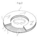
- Fig. 2 schematically shows the essential configuration of a rotary electrostatic motor.
- the illustrated rotary electrostatic motor has substantially the same configuration as that of the linear electrostatic motor of Fig. 1 except that a plurality of multi-phase electrodes 3 are arranged radially at regular intervals, and thus the corresponding components are denoted by the same reference numerals.
- a stationary member 1, formed from a film-like electrode member, includes a plurality of multi-phase electrodes 3 formed, e.g., as electrically conductive strip-shaped thin films or thin wires, which are embedded in an insulator 4 in a radial arrangement at predetermined regular intervals.
- a multi-phase AC power source is also connected respectively to the stationary member 1 and the movable member 2, so as to generate traveling-wave electric fields, whereby the movable member 2 undergoes a rotary motion (shown by an arrow) relative to the stationary member 1 due to the traveling-wave electric fields.
- it is also possible to produce a laminated-type rotary electrostatic motor by stacking plural sets of stationary and movable members, each set including mutually opposed stationary member 1 and movable member 2, for the purpose of increasing an output power.
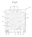
- Fig. 3 illustrates a conductor pattern in the film-like electrode member constituting each of the stationary member 1 and the movable member 2 in the linear electrostatic motor of Fig. 1.
- a conductor pattern represented by a solid line is provided along the major surface of the insulator 4, and a conductor pattern represented by a broken line is provided along the back surface of the insulator 4.
- the insulator 4 of the stationary member 1 is provided with a plurality of electrodes 3 (3a, 3b, 3c) driven by a three-phase AC power source, plated through-hole type electrically conductive portions 6a, 6b, 6c connected respectively to the first, second and third phases of the three-phase AC power source, and current paths 5a, 5b, 5c for respectively connecting the electrically conductive portions 6a, 6b, 6c to the respective-phase electrodes 3a, 3b, 3c.
- the plural (five, in the drawing) second-phase electrodes 3b, 3b, ... are connected through the currant path 5b to the through-hole conductive portion 6b connected to the second phase of the power source, and the plural (five, in the drawing) third-phase electrodes 3c, 3c, ... are connected through the current path 5c to the through-hole conductive portion 6c connected to the third phase of the power source.
- the first and second-phase current paths 5a, 5b are disposed along the major surface of the insulator 4, while the third-phase current path 5c is disposed along the back surface of the insulator 4 and is connected to the third-phase electrode 3c via another through-hole electrically conductive portion 7.
- the film-like electrode member 10 is provided with an insulating substrate 12 including a major surface 12a and a back surface 12b opposite to the major surface 12a; a plurality of electrodes 14 arranged along the major surface 12a of the insulating substrate 12 at predetermined intervals; a main section 16 including at least a part of the plural electrodes 14 and of the insulating substrate 12 carrying the electrodes 14; a local thick section 18 integrally joined to the main section 16 and having a thickness larger than the thickness of the main section 16; and a conducting element 20 formed on the thick section 18 and connected to the plural electrodes 14.
- the thick section 18 includes a protrusion element 22 having insulating properties and locally protruding from the major surface 12a of the insulating substrate 12.
- the conducting element 20 is formed continuously on both the insulating substrate 12 and the protrusion element 22.
- the thick section 18 is also provided with a through hole 24 perforating across the thickness of the thick section 18.
- the conducting element 20 includes a metal coat 26 formed on the wall surface of the through hole 24 and a land portion 28 formed at a side of at least one (both, in the drawing) of the major surface 12a and the back surface 12b of the insulating substrate 12.
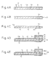
- a base material 32 e.g., a copper-clad laminate, as a base material of a flexible printed board
- the base material 32 is provided with at least one (or a desired number of) through hole 34 usable for a power-source connection (i.e., a hole for forming each of the through-hole conductive portions 6a to 6c, 7 in Fig. 3) formed at predetermined positions (Fig. 4A).
- the inner surface of the through hole 34 is plated to form a through-hole plating 34a (Fig. 4B).
- a plurality of electrodes 14 i.e., electrodes 3a to 3c in Fig. 3 for driving purposes and other conductors (i.e., current paths 5a to 5c in Fig. 3) are formed at one time, after resist applying, patterning and etching steps.
- an annular conductive portion 34b connected to the through-hole plating 34a is formed, for the through hole 34 corresponding to each of the through-hole conductive portions 6a to 6c of Fig. 3, on the back surface 12b of the insulating substrate 12 (Fig. 4C).
- a protrusion element 22 made of a film having electrically insulating property which acts as a spacer for maintaining a required small clearance between the opposing film-like electrode members 10 when a plurality of film-like electrode members 10 are stacked.
- An electrically conductive layer 36 is previously formed on one surface of the protrusion element 22, and at least one (or a desired number of) through hole 38, the location of which corresponds to the location of the through hole 34 in the insulating substrate 12, is previously formed in the protrusion element 22 so as to perforate through the conductive layer 36 by a desired perforating process.
- the protrusion element 22 is adhered to the major surface 12a of the insulating substrate 12 by an adhesive 40, with the through hole 38 of the protrusion element 22 being aligned to the through hole 34 of the insulating substrate 12. Consequently, the thick section 18 provided with the through hole 24 (i.e., a hole corresponding to each of the through-hole conductive portions 6a to 6c of Fig. 3) is formed (Fig. 4D).
- the through hole 24 in the thick section 18 is twice plated.
- the through-hole plating 34a of the insulating substrate 12 is integrally coupled with the through-hole plating 38a of the protrusion element 22, so as to form the metal coat 26 of the conducting element 20, and thus the protrusion element 22 constituting a spacer is electrically connected to a conductor (including the plural electrodes 14) provided on the insulating substrate 12.
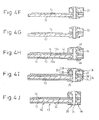
- cover films 44 are attached to both surfaces 12a, 12b of the insulating substrate 12 in an air-tight manner, to constitute an integrated member, by adhesion, coating or surface activation.
- Each cover film 44 is provided with an opening 46 previously formed at a location corresponding to the location of the through hole 24 of the thick section 18 (Fig. 4H).
- a layer, thicker than the cover film 44 is plated onto a region of the opening 46 of each cover film 44, so as to form the annular land portion 28 projecting outward from each cover film 44. Consequently, the conducting element 20 including the metal coat 26 and the pair of land portions 28, integrally coupled with each other, is formed on the thick section 18 including the through hole 24 including the through hole 34 in the insulating substrate 12 and the through hole 38 in the protrusion element 22, communicated with each other (Fig. 41).
- the through hole 24 in the thick section 18, for which the conducting element 20 is provided corresponds to each of the through-hole conductive portions 6a to 6c in Fig. 3.
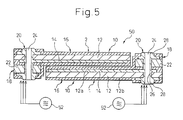
- the film-like electrode member 10 produced through the above steps is used for each of the stationary member 1 and the movable member 2, and the stationary member 1 and the movable member 2 are arranged to be opposed to each other in a relatively movable manner through a small clearance defined therebetween, so that an electrostatic motor 50, as a base unit, according to an embodiment of the present invention is produced.
- a voltage is individually applied to the respective conducting elements of the stationary member 1 and the movable member 2, so as to generate positive and negative electrostatic forces between the respective sets of electrodes 14 of the members 1, 2, and thus to ensure a propelling or rotating power of the movable member 2 relative to the stationary member 1.
- a multi-phase AC power source 52 in which voltage levels are sequentially varied, is used to individually apply the voltage to the conducting elements 20 of the stationary and movable members 1, 2.
- the multi-phase AC power source 52 for the stationary member 1 and the multi-phase AC power source 52 for the movable member 2 may be constituted from the same one. In this case, the phase orders, of the respective voltages applied to the stationary member 1 and the movable member 2, are mutually reversed. Also, from a practical viewpoint, it is desirable that the multi-phase AC power source 52 is a three-phase AC power source.
- a plurality of stationary members 1 and a plurality of movable members 2, each of which is constructed from the film-like electrode member 10, are assembled together in a manner that the respective stationary members 1 and the respective movable members 2 are alternately arranged, so that a laminated high-power type electrostatic motor 60 according to another embodiment of the present invention is produced.
- a stationary-member stack 62 including two stationary members 1 and a movable-member stack 64 including two movable members 2 are arranged so that the members 1, 2 are alternately stacked in the direction of thickness of the film-like electrode member 10.
- the stationary-member stack 62 including two stationary members 1 are configured in a manner that the major surface 12a of the insulating substrate 12 of a first stationary member 1 is disposed to be opposed to the back surface 12b of the insulating substrate 12 of a second stationary member 1, and that the thick sections 18 of the first and second stationary members 1 are brought into abutment with each other while maintaining a positional alignment therebetween.
- the thickness T1 of the thick section 18 of each stationary member 1 is dimensioned so as to form a gap between the main sections 16 of the first and second stationary members 1, the gap being capable of receiving the main section 16 of one movable member 2 in a condition free from contact.
- conductive contact is accomplished between the land portion 28 of the conducting element 20 located at a side of the major surface 12a of the first stationary member 1 and the land portion 28 of the conducting element 20 located at a side of the back surface 12b of the second stationary member 1.
- the movable-member stack 64 including two movable members 2 are configured in a manner that the major surface 12a of the insulating substrate 12 of a first movable member 2 is disposed to be opposed to the back surface 12b of the insulating substrate 12 of a second movable member 2, and that the thick sections 18 of the first and second movable members 2 are brought into abutment with each other while maintaining a positional alignment therebetween.
- the thickness T2 of the thick section 18 of each movable member 2 is dimensioned so as to form a gap between the main sections 16 of the first and second movable members 2, the gap being capable of receiving the main section 16 of one stationary member 1 in a condition free from contact.
- conductive contact is accomplished between the land portion 28 of the conducting element 20 located at a side of the major surface 12a of the first movable member 2 and the land portion 28 of the conducting element 20 located at a side of the back surface 12b of the second movable member 2.
- the thick section 18 of each film-like electrode element 10 functions as a spacer so as to create and maintain a suitable small clearance between the main sections 16 of the stationary and movable members 1, 2.
- the land portions 28 formed to project outwards on the thick sections 18 of the respective film-like electrode elements 10 come into conductive contact with each other, so that an electric connection between the stationary members 1 and an electric connection between the movable members 2 are established.
- the stationary-member stack 62 and the movable-member stack 64 are to be produced, it is required only that a plurality of film-like electrode members 10 are mutually aligned and stacked while applying a pressure thereto in a thickness direction, so as to connect the conducting elements 20 having through holes 24 (corresponding to each of the through-hole conductive portions 6a to 6c in Fig.
- the stationary-member stack 62 may be provided with a first connection member 66 inserted into the through holes 24 of the thick sections 18 of the stacked stationary members 1 to electrically connect the stationary members 1 with each other.
- the movable-member stack 64 may be provided with a second connection member 68 inserted into the through holes 24 of the thick sections 18 of the stacked movable members 2 to electrically connect the movable members 2 with each other.
- the first and second connection members 66 and 68 may be constituted by, e.g., electrically conducting pins as illustrated.
- the first and second connection members 66, 68 improve the reliability of the mutual electric connection through the land portions 28 of the opposing stationary members 1 as well as of the opposing movable members 2, provided that the through holes 24 and the metal coats 26 of the conducting elements 20 in the respective stationary and movable members 1, 2 are formed with a sufficiently high precision. Further, the first and second connection members 66, 68 contribute to the mutual positioning of the stacked stationary members 1 as well as of the stacked movable members 2.
- an electrostatic motor such as the above-described electrostatic motor 60, in which a plurality of stationary members are connected to each other in a parallel stacked arrangement and also a plurality of movable members are connected to each other in a parallel stacked arrangement
- the performance of the motor is affected by a mechanical positional deviation (particularly, a positional deviation in a driving direction) between the stacked stationary members and between the stacked movable members.
- the land portions 28 of the film-like electrode member 10 constituting each of the stationary members 1 and the movable members are formed by metal platings, so that mechanical connections in the stationary-member stack 62 and in the movable-member stack 64 exhibit a high rigidity not only in a thickness direction but also in a driving direction. Therefore, it is possible to effectively decrease the positional deviation of the plural stationary and movable members 1, 2 during an assembling process and also during a driving operation.
- the film-like electrode members 10 for the stationary members 1 and the movable members 2, as the essential components in the electrostatic motor 60 can be produced on the basis of a printed-circuit board manufacturing technique, so that it is possible to easily ensure the precision and stability of a producing process. Furthermore, as for the laminating and assembling process of the plural film-like electrode members 10, the problems in the prior art, such as the deterioration in precision caused by the use of a separate spacer, is overcome, due to the use of the film-like electrode member 10 provided integrally with the thick section 18 acting as a spacer instead of using the separate spacer, which readily improve the precision of assembling steps.
- the film-like electrode member 10 having a spacer function establishes a large thickness of a film structure, which results in a high rigidity of the electrode member 10, and it is thus possible to suppress the deterioration of an assembling precision, which is otherwise caused by the warp of the film-like electrode members 10 during an assembling process.
- the film-like electrode member 10 provided integrally or unitarily with the thick section 18 has a weight somewhat larger than a conventional film-like electrode member, and thereby eliminates the disadvantage of displacement of the electrode member 10 due to an unintentional operation during the assembling process.
- connection members 66, 68 such as the electrically conducting pins, as described above.
- patterning and etching steps can result in a highly precise positioning, but through-hole drilling and hole inner-surface plating steps may sometimes result in an unsatisfactory precision.
- the stationary-member stack 62 and the movable-member stack 64 are assembled without using the connection members 66, 68, which may improve the assembling precision and result in good products.
- Fig. 8 illustrates a film-like electrode member 70 according to another embodiment of the present invention.
- the film-like electrode member 70 has a configuration substantially identical to that of the above-described film-like electrode member 10, except for a different feature in a stacked configuration depending upon a different producing process. Therefore, corresponding components are denoted by common reference numerals, and the description thereof is not repeated.
- the film-like electrode member 70 is produced in a manner as described below.
- a plurality of electrodes 14 for driving purposes (corresponding to the electrodes 3a to 3c in Fig. 3) and other conductors (corresponding to the current paths 5a to 5c in Fig. 3) are formed on a film-like insulating substrate 12 having an electrically conductive layer (corresponding to the base material 32 in Fig. 4A) at one time, via patterning and etching steps, without forming a through hole 34 (Fig. 4A).
- cover films 44 are attached to both surfaces 12a, 12b of the insulating substrate 12 in an air-tight manner to constitute an integrated member, by an adhesion, a coating or a surface activation, so as to constitute a first film member.
- an electrically conductive portion 36' is formed on a film-like protrusion element 22 having an electrically conductive layer, via patterning and etching steps, without forming a through hole 38 (Fig. 4D).
- cover films 44' are attached to both surfaces of the protrusion element 22, so as to constitute a second film member functioning as a spacer.
- the second film member is affixed onto the first film member by using an adhesive 40, so as to form a thick section 18.
- the thick section 18 is subjected to a drilling step to form a through hole 24, and the through hole 24 and the peripheral area of the opening thereof are plated, so as to constitute a conducting element 20 including a metal coat 26 and a pair of land portions 28.
- the film-like electrode member 70 provided with the thick section 18 having the through hole 24, to which the conducting element 20 is formed, (corresponding to each of the through-hole conductive portions 6a to 6c in Fig. 3) is produced.
Landscapes
- Micromachines (AREA)
Applications Claiming Priority (2)
| Application Number | Priority Date | Filing Date | Title |
|---|---|---|---|
| JP2004016083 | 2004-01-23 | ||
| JP2004016083A JP3886494B2 (ja) | 2004-01-23 | 2004-01-23 | 固定子用及び移動子用のフィルム型電極及び静電モータ |
Publications (2)
| Publication Number | Publication Date |
|---|---|
| EP1557938A2 true EP1557938A2 (de) | 2005-07-27 |
| EP1557938A3 EP1557938A3 (de) | 2007-05-09 |
Family
ID=34631956
Family Applications (1)
| Application Number | Title | Priority Date | Filing Date |
|---|---|---|---|
| EP05001114A Withdrawn EP1557938A3 (de) | 2004-01-23 | 2005-01-20 | Filmähnliche Elektrode für elektrostatischer Mikromotor |
Country Status (3)
| Country | Link |
|---|---|
| US (1) | US7388315B2 (de) |
| EP (1) | EP1557938A3 (de) |
| JP (1) | JP3886494B2 (de) |
Cited By (1)
| Publication number | Priority date | Publication date | Assignee | Title |
|---|---|---|---|---|
| EP2040366A4 (de) * | 2006-06-16 | 2012-07-04 | Shinsei Corp | Elektrostatischer motor |
Families Citing this family (3)
| Publication number | Priority date | Publication date | Assignee | Title |
|---|---|---|---|---|
| JP4015119B2 (ja) * | 2004-01-23 | 2007-11-28 | ファナック株式会社 | 静電モータ |
| JP3886494B2 (ja) * | 2004-01-23 | 2007-02-28 | ファナック株式会社 | 固定子用及び移動子用のフィルム型電極及び静電モータ |
| US10951132B2 (en) * | 2016-05-17 | 2021-03-16 | Wisconsin Alumni Research Foundation | Electrostatic rotating-machine employing dielectric substrates with surface conductors |
Family Cites Families (14)
| Publication number | Priority date | Publication date | Assignee | Title |
|---|---|---|---|---|
| JPH0365084A (ja) * | 1989-08-02 | 1991-03-20 | Hitachi Ltd | 静電型2次元アクチュエータ,光ヘツドおよび光デイスク装置 |
| WO1991016757A1 (en) * | 1990-04-16 | 1991-10-31 | Fujitsu Limited | Electrostatic actuator |
| US5189323A (en) * | 1991-12-19 | 1993-02-23 | The Trustees Of Princeton University | Rotary, vertical-drive, tethered micromotor |
| JPH0678566A (ja) * | 1992-08-25 | 1994-03-18 | Kanagawa Kagaku Gijutsu Akad | 静電アクチュエータ |
| AU2268295A (en) * | 1994-04-16 | 1995-11-10 | Jae Hwan Kim | A system for generating power and propulsive force or lift by use of an electrostatic motor |
| JPH08266071A (ja) * | 1995-03-23 | 1996-10-11 | Toshiro Higuchi | 多軸駆動装置 |
| JPH0937569A (ja) * | 1995-07-19 | 1997-02-07 | Tomoaki Abiko | 絶縁多層電界モータ |
| KR100398856B1 (ko) * | 2000-03-30 | 2003-09-19 | 가부시끼가이샤 도시바 | 정전 액튜에이터 기구, 그 구동 방법, 및 그것을 이용한카메라 모듈 |
| US6619999B2 (en) * | 2000-12-28 | 2003-09-16 | Tyco Electronics Corporation | Solderless connector for opto-electric module |
| JP4015119B2 (ja) * | 2004-01-23 | 2007-11-28 | ファナック株式会社 | 静電モータ |
| JP3886494B2 (ja) * | 2004-01-23 | 2007-02-28 | ファナック株式会社 | 固定子用及び移動子用のフィルム型電極及び静電モータ |
| JP4027327B2 (ja) * | 2004-01-23 | 2007-12-26 | ファナック株式会社 | 静電モータ |
| JP4146813B2 (ja) * | 2004-03-25 | 2008-09-10 | ファナック株式会社 | 静電モータ |
| JP2006101631A (ja) * | 2004-09-29 | 2006-04-13 | Fanuc Ltd | 静電モータ及びその製造方法 |
-
2004
- 2004-01-23 JP JP2004016083A patent/JP3886494B2/ja not_active Expired - Fee Related
-
2005
- 2005-01-20 EP EP05001114A patent/EP1557938A3/de not_active Withdrawn
- 2005-01-21 US US11/038,224 patent/US7388315B2/en not_active Expired - Fee Related
Cited By (3)
| Publication number | Priority date | Publication date | Assignee | Title |
|---|---|---|---|---|
| EP2040366A4 (de) * | 2006-06-16 | 2012-07-04 | Shinsei Corp | Elektrostatischer motor |
| US8278797B2 (en) | 2006-06-16 | 2012-10-02 | Shinsei Corporation | Electrostatic motor |
| US8779647B2 (en) | 2006-06-16 | 2014-07-15 | Shinsei Corporation | Electrostatic motor |
Also Published As
| Publication number | Publication date |
|---|---|
| JP3886494B2 (ja) | 2007-02-28 |
| US20050162037A1 (en) | 2005-07-28 |
| EP1557938A3 (de) | 2007-05-09 |
| US7388315B2 (en) | 2008-06-17 |
| JP2005210851A (ja) | 2005-08-04 |
Similar Documents
| Publication | Publication Date | Title |
|---|---|---|
| EP0030008B1 (de) | Spule für Kleinstmotor | |
| US7521836B2 (en) | Electrostatic actuator with fault tolerant electrode structure | |
| US7291956B2 (en) | Laminate coil and brushless motor using same | |
| US7233096B2 (en) | Multilayer piezoelectric element and vibration-wave drive device | |
| JP2899133B2 (ja) | 静電アクチュエータ | |
| CN112470381A (zh) | 平面马达定子 | |
| US7230364B2 (en) | Electrostatic motor utilizing static electricity as a drive force | |
| US7388315B2 (en) | Film-like electrode member with local thick section for assembling and positioning purposes, and electrostatic motor having the same | |
| US5632074A (en) | Vibration wave driven motor | |
| US7372186B2 (en) | Electrostatic motor with clearance maintaining structure | |
| JP2899120B2 (ja) | 静電アクチュエータ | |
| JP2003174749A (ja) | 積層セラミックコイルおよびこれを用いたモータ | |
| JP4386767B2 (ja) | 高分子アクチュエータを用いた電気素子 | |
| US7518282B2 (en) | Rotor, vibration motor having the same, and fabrication method thereof | |
| JPS63262038A (ja) | Fgコイル付きモ−タ用プリントコイル | |
| JP2005333716A (ja) | 静電アクチュエータ用エレクトレットフィルムの製造方法 | |
| JP3470832B2 (ja) | 静電アクチュエータにおける多層電極配線板、及びその製造方法 | |
| JP2979569B2 (ja) | 静電アクチュエータ | |
| JP2978892B1 (ja) | 編機選針用圧電アクチュエータ | |
| JPH07222464A (ja) | 静電アクチュエータ | |
| JP2628872B2 (ja) | 偏平ブラシレスモータ用コイル | |
| JP2000110055A (ja) | 編機用選針装置 | |
| JPS61273141A (ja) | 同期電動機用デイスク状ステ−タエレメント | |
| JPS61254048A (ja) | 同期電動機用デイスク状ステ−タエレメントの製造方法 | |
| JP2000295875A (ja) | 積層型圧電アクチュエータおよびこれを用いた超音波モータ |
Legal Events
| Date | Code | Title | Description |
|---|---|---|---|
| PUAI | Public reference made under article 153(3) epc to a published international application that has entered the european phase |
Free format text: ORIGINAL CODE: 0009012 |
|
| AK | Designated contracting states |
Kind code of ref document: A2 Designated state(s): AT BE BG CH CY CZ DE DK EE ES FI FR GB GR HU IE IS IT LI LT LU MC NL PL PT RO SE SI SK TR |
|
| AX | Request for extension of the european patent |
Extension state: AL BA HR LV MK YU |
|
| PUAL | Search report despatched |
Free format text: ORIGINAL CODE: 0009013 |
|
| AK | Designated contracting states |
Kind code of ref document: A3 Designated state(s): AT BE BG CH CY CZ DE DK EE ES FI FR GB GR HU IE IS IT LI LT LU MC NL PL PT RO SE SI SK TR |
|
| AX | Request for extension of the european patent |
Extension state: AL BA HR LV MK YU |
|
| 17P | Request for examination filed |
Effective date: 20070716 |
|
| AKX | Designation fees paid |
Designated state(s): DE |
|
| STAA | Information on the status of an ep patent application or granted ep patent |
Free format text: STATUS: THE APPLICATION HAS BEEN WITHDRAWN |
|
| 18W | Application withdrawn |
Effective date: 20090128 |