EP1560334A1 - Frequenzteiler - Google Patents
Frequenzteiler Download PDFInfo
- Publication number
- EP1560334A1 EP1560334A1 EP05100257A EP05100257A EP1560334A1 EP 1560334 A1 EP1560334 A1 EP 1560334A1 EP 05100257 A EP05100257 A EP 05100257A EP 05100257 A EP05100257 A EP 05100257A EP 1560334 A1 EP1560334 A1 EP 1560334A1
- Authority
- EP
- European Patent Office
- Prior art keywords
- flip
- flops
- divider
- flop
- frequency
- Prior art date
- Legal status (The legal status is an assumption and is not a legal conclusion. Google has not performed a legal analysis and makes no representation as to the accuracy of the status listed.)
- Granted
Links
- 238000005516 engineering process Methods 0.000 description 2
- 235000021183 entrée Nutrition 0.000 description 2
- 230000009466 transformation Effects 0.000 description 2
- 230000007704 transition Effects 0.000 description 2
- 230000015572 biosynthetic process Effects 0.000 description 1
- 230000008030 elimination Effects 0.000 description 1
- 238000003379 elimination reaction Methods 0.000 description 1
- 238000003786 synthesis reaction Methods 0.000 description 1
- 238000000844 transformation Methods 0.000 description 1
Images

Classifications
-
- H—ELECTRICITY
- H03—ELECTRONIC CIRCUITRY
- H03K—PULSE TECHNIQUE
- H03K23/00—Pulse counters comprising counting chains; Frequency dividers comprising counting chains
- H03K23/40—Gating or clocking signals applied to all stages, i.e. synchronous counters
- H03K23/50—Gating or clocking signals applied to all stages, i.e. synchronous counters using bi-stable regenerative trigger circuits
- H03K23/54—Ring counters, i.e. feedback shift register counters
- H03K23/544—Ring counters, i.e. feedback shift register counters with a base which is an odd number
-
- H—ELECTRICITY
- H03—ELECTRONIC CIRCUITRY
- H03K—PULSE TECHNIQUE
- H03K23/00—Pulse counters comprising counting chains; Frequency dividers comprising counting chains
- H03K23/64—Pulse counters comprising counting chains; Frequency dividers comprising counting chains with a base or radix other than a power of two
- H03K23/66—Pulse counters comprising counting chains; Frequency dividers comprising counting chains with a base or radix other than a power of two with a variable counting base, e.g. by presetting or by adding or suppressing pulses
- H03K23/665—Pulse counters comprising counting chains; Frequency dividers comprising counting chains with a base or radix other than a power of two with a variable counting base, e.g. by presetting or by adding or suppressing pulses by presetting
Definitions
- the invention relates to a device for dividing the frequency at least 3 rows.
- the known head dividers of the prior art are generally divisors with 2 consecutive division ranks.
- a multiplexer comprises for example 2 inputs, 1 bit of selection, 1 output and in that it is integrated in a rocker.
- the device may comprise 2 latches (U 4 , U 5 ) and 2 multiplexers (M 4 , M 5 ), respectively receiving the inputs INC1 and INC2 of the divider.
- the multiplexer can be integrated into a flip-flop.
- the invention particularly has the following advantages: operating frequency is maximum because the loopback paths between a flip-flop output D and its input or the input of another flip-flop D are minimal in terms of the number of logical layers. These paths do not comprise, in normal operation, a single multiplexer.
- the multiplexer is integrated or integrable with flip-flop D depending on the technology.
- the following example relates to a divider with 3 rows.
- the principle also applies to divisors of frequency to more than 3 rows, 4, 5, etc.
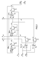
- Figure 1 shows a frequency divider dividing by 3 ranks, ranks 2, 3 and 4, a frequency F e .
- the choice between the three ranks of division is made by means of a control bus composed of 2 bits referenced P1 and P2.
- Any flip-flop having an output that stores the value of the input at the moment of the clock transition (positive or negative clock edge) can also be used to replace a D flip-flop.
- multiplexer is meant, in the present description, a multiplexer or any other device that has one or several signal inputs, a selection input and an output that copies the value of one of the signal inputs according to the value of the selection command.
- the 3 flip-flops operate on the same clock F e .
- Table 1 below groups the division rank values obtained by the divider of FIG. 1.
- P1 P2 Division rank obtained according to P1 and P2 0 1
- the circuit divides by 2 1 0
- the circuit divides by 3 1 1
- the divider also comprises, for example, 2 latches U 4 , U 5 and 2 multiplexers M 4 , M 5 , respectively receiving the inputs INC1 and INC2 of the divider.
- the 2 latchs can be replaced by 2 scales or any other device with the same function.
- the operation of the divider is given in Table 2 below. INC1 INC2 0 0 The circuit divides by 2 1 0 The circuit divides by 3 0 1 The circuit divides by 3 1 1 The circuit divides by 4
- one of the D flip-flops controls the loading of the 3 flip-flops U 1 , U 2 , U 3 during a period of the clock F e . This operation is optimal from the point of view of the positioning time for the P1 and P2 commands and the elimination of false cycles.
- Q1 has a low state of duration equal to a single period of F e for the 3 ranks of division. This low state is for example located at the end of the cycle of Q1. This characteristic is exploited when this circuit is used as a head divider in a dividing chain by giving a possibility of selecting a single edge of the frequency F e by the output cycle of the head divider.
- each D flip-flop is decomposed into at least 2 latches.
- Another variant is to keep the same equations logic giving Q1, Q2 and Q3 which are characteristic of the circuit and their apply usual logical transformations.
- An example of transformation consists of complementing the 2 parts of each equation.
- any flip-flop whose output memorizes the value of the input at the moment of the clock transition (front positive or negative clock) can be used in the divider according to the invention.
Landscapes
- Stabilization Of Oscillater, Synchronisation, Frequency Synthesizers (AREA)
- Manipulation Of Pulses (AREA)
- Soil Working Implements (AREA)
- Control Of Motors That Do Not Use Commutators (AREA)
- Charge And Discharge Circuits For Batteries Or The Like (AREA)
Applications Claiming Priority (2)
| Application Number | Priority Date | Filing Date | Title |
|---|---|---|---|
| FR0400496 | 2004-01-20 | ||
| FR0400496A FR2865327B1 (fr) | 2004-01-20 | 2004-01-20 | Diviseur de frequence |
Publications (2)
| Publication Number | Publication Date |
|---|---|
| EP1560334A1 true EP1560334A1 (de) | 2005-08-03 |
| EP1560334B1 EP1560334B1 (de) | 2009-10-21 |
Family
ID=34639781
Family Applications (1)
| Application Number | Title | Priority Date | Filing Date |
|---|---|---|---|
| EP05100257A Expired - Lifetime EP1560334B1 (de) | 2004-01-20 | 2005-01-17 | Frequenzteiler |
Country Status (5)
| Country | Link |
|---|---|
| US (1) | US7218699B2 (de) |
| EP (1) | EP1560334B1 (de) |
| AT (1) | ATE446610T1 (de) |
| DE (1) | DE602005017211D1 (de) |
| FR (1) | FR2865327B1 (de) |
Families Citing this family (4)
| Publication number | Priority date | Publication date | Assignee | Title |
|---|---|---|---|---|
| FR2880219B1 (fr) * | 2004-12-23 | 2007-02-23 | Thales Sa | Procede et systeme de radiocommunication numerique, notamment pour les stations sol mobiles |
| TWI393344B (zh) * | 2009-04-22 | 2013-04-11 | Univ Nat Taiwan | 多除頻模式毫米波除頻電路 |
| CN102427363B (zh) * | 2011-12-23 | 2015-02-04 | 上海贝岭股份有限公司 | 一种小分频系数的多相多模分频电路 |
| US10075308B2 (en) | 2016-09-30 | 2018-09-11 | Intel Corporation | Supply voltage adaptation via decision feedback equalizer |
Citations (3)
| Publication number | Priority date | Publication date | Assignee | Title |
|---|---|---|---|---|
| JPH01157616A (ja) * | 1987-12-14 | 1989-06-20 | Fujitsu Ltd | 同期式リングカウンタ |
| JPH09107284A (ja) * | 1995-05-24 | 1997-04-22 | He Holdings Inc Dba Hughes Electron | 高速同期カウンタ回路 |
| JPH09289445A (ja) * | 1996-04-23 | 1997-11-04 | Sharp Corp | 同期式カウンタ |
Family Cites Families (3)
| Publication number | Priority date | Publication date | Assignee | Title |
|---|---|---|---|---|
| JP2841110B2 (ja) * | 1990-07-30 | 1998-12-24 | チッソ株式会社 | α―クロロケトン類の製造法 |
| FR2734966B1 (fr) * | 1995-05-31 | 1997-08-14 | Sgs Thomson Microelectronics | Diviseur programmable rapide |
| US5808691A (en) * | 1995-12-12 | 1998-09-15 | Cirrus Logic, Inc. | Digital carrier synthesis synchronized to a reference signal that is asynchronous with respect to a digital sampling clock |
-
2004
- 2004-01-20 FR FR0400496A patent/FR2865327B1/fr not_active Expired - Fee Related
-
2005
- 2005-01-17 DE DE602005017211T patent/DE602005017211D1/de not_active Expired - Lifetime
- 2005-01-17 AT AT05100257T patent/ATE446610T1/de not_active IP Right Cessation
- 2005-01-17 EP EP05100257A patent/EP1560334B1/de not_active Expired - Lifetime
- 2005-01-21 US US11/038,487 patent/US7218699B2/en not_active Expired - Fee Related
Patent Citations (3)
| Publication number | Priority date | Publication date | Assignee | Title |
|---|---|---|---|---|
| JPH01157616A (ja) * | 1987-12-14 | 1989-06-20 | Fujitsu Ltd | 同期式リングカウンタ |
| JPH09107284A (ja) * | 1995-05-24 | 1997-04-22 | He Holdings Inc Dba Hughes Electron | 高速同期カウンタ回路 |
| JPH09289445A (ja) * | 1996-04-23 | 1997-11-04 | Sharp Corp | 同期式カウンタ |
Non-Patent Citations (3)
| Title |
|---|
| PATENT ABSTRACTS OF JAPAN vol. 013, no. 421 (E - 822) 19 September 1989 (1989-09-19) * |
| PATENT ABSTRACTS OF JAPAN vol. 1998, no. 03 27 February 1998 (1998-02-27) * |
| PATENT ABSTRACTS OF JAPAN vol. 1999, no. 07 31 March 1999 (1999-03-31) * |
Also Published As
| Publication number | Publication date |
|---|---|
| US7218699B2 (en) | 2007-05-15 |
| EP1560334B1 (de) | 2009-10-21 |
| FR2865327B1 (fr) | 2006-02-24 |
| US20050179475A1 (en) | 2005-08-18 |
| DE602005017211D1 (de) | 2009-12-03 |
| FR2865327A1 (fr) | 2005-07-22 |
| ATE446610T1 (de) | 2009-11-15 |
Similar Documents
| Publication | Publication Date | Title |
|---|---|---|
| US6300809B1 (en) | Double-edge-triggered flip-flop providing two data transitions per clock cycle | |
| FR2563955A1 (fr) | Circuit retardateur de signaux numeriques | |
| FR2638869A1 (fr) | Dispositif de securite contre la detection non autorisee de donnees protegees | |
| WO2009013422A2 (fr) | Cellule logique reconfigurable a base de transistors mosfet double grille | |
| EP0746109A1 (de) | Schneller programmierbaren Teiler | |
| EP1560334B1 (de) | Frequenzteiler | |
| EP3595234A1 (de) | Schieberegister, das gegen physische angriffe geschützt ist | |
| EP1241788A1 (de) | Digitaler Frequenzteiler | |
| EP1111783B1 (de) | Gesicherte Typ D Master-Slave Kippschaltung | |
| EP0477099B1 (de) | Schutzschaltung für eine Flüssigkristallanzeigetreibeschaltung | |
| FR2898223A1 (fr) | Circuit de distribution d'un signal initial a structure en arbre protege contre les aleas logiques. | |
| KR910014949A (ko) | 시프트 레지스터 | |
| FR2645294A1 (fr) | Montage multiplicateur de mots numeriques en serie | |
| FR2729500A1 (fr) | Systeme d'acquisition de donnees a grande vitesse | |
| EP0658838B1 (de) | Frequenzsynthetisierer | |
| FR2774188A1 (fr) | Circuit de verification de parite | |
| EP1742407B1 (de) | Kopierschutz von digitalen Daten innerhalb einer integrierte Schaltung mit JTAG Anschluss | |
| FR2788353A1 (fr) | Microprocesseur avec circuits de protection pour securiser l'acces a ses registres | |
| FR2604577A1 (fr) | Circuit generateur de code a bruit pseudo-aleatoire | |
| FR2653950A1 (fr) | Systeme de generation de train de donnees. | |
| CH622901A5 (de) | ||
| FR2575880A1 (fr) | Diviseur de frequences | |
| EP0889481A1 (de) | Verbesserungen von Speicherschaltungen mit sequentiellem Zugriff | |
| EP0648018B1 (de) | Schaltung zur Anzeige der Phasenverhältnisse zwischen mehreren Signalen mit gleicher Frequenz und ihre Anwendung in einer Schaltung zur Korrektur der Phasen zwischen diesen Signalen | |
| EP0186533A1 (de) | Dynamisches Speicherelement und seine Verwendung in einer Master-Slave-Kippschaltung und in programmierbaren sequentiellen Schaltungen |
Legal Events
| Date | Code | Title | Description |
|---|---|---|---|
| PUAI | Public reference made under article 153(3) epc to a published international application that has entered the european phase |
Free format text: ORIGINAL CODE: 0009012 |
|
| AK | Designated contracting states |
Kind code of ref document: A1 Designated state(s): AT BE BG CH CY CZ DE DK EE ES FI FR GB GR HU IE IS IT LI LT LU MC NL PL PT RO SE SI SK TR |
|
| AX | Request for extension of the european patent |
Extension state: AL BA HR LV MK YU |
|
| 17P | Request for examination filed |
Effective date: 20060111 |
|
| AKX | Designation fees paid |
Designated state(s): AT BE BG CH CY CZ DE DK EE ES FI FR GB GR HU IE IS IT LI LT LU MC NL PL PT RO SE SI SK TR |
|
| GRAP | Despatch of communication of intention to grant a patent |
Free format text: ORIGINAL CODE: EPIDOSNIGR1 |
|
| GRAS | Grant fee paid |
Free format text: ORIGINAL CODE: EPIDOSNIGR3 |
|
| GRAA | (expected) grant |
Free format text: ORIGINAL CODE: 0009210 |
|
| AK | Designated contracting states |
Kind code of ref document: B1 Designated state(s): AT BE BG CH CY CZ DE DK EE ES FI FR GB GR HU IE IS IT LI LT LU MC NL PL PT RO SE SI SK TR |
|
| REG | Reference to a national code |
Ref country code: GB Ref legal event code: FG4D Free format text: NOT ENGLISH |
|
| REG | Reference to a national code |
Ref country code: CH Ref legal event code: EP |
|
| REG | Reference to a national code |
Ref country code: IE Ref legal event code: FG4D |
|
| REF | Corresponds to: |
Ref document number: 602005017211 Country of ref document: DE Date of ref document: 20091203 Kind code of ref document: P |
|
| REG | Reference to a national code |
Ref country code: SE Ref legal event code: TRGR |
|
| LTIE | Lt: invalidation of european patent or patent extension |
Effective date: 20091021 |
|
| PG25 | Lapsed in a contracting state [announced via postgrant information from national office to epo] |
Ref country code: PT Free format text: LAPSE BECAUSE OF FAILURE TO SUBMIT A TRANSLATION OF THE DESCRIPTION OR TO PAY THE FEE WITHIN THE PRESCRIBED TIME-LIMIT Effective date: 20100222 Ref country code: LT Free format text: LAPSE BECAUSE OF FAILURE TO SUBMIT A TRANSLATION OF THE DESCRIPTION OR TO PAY THE FEE WITHIN THE PRESCRIBED TIME-LIMIT Effective date: 20091021 Ref country code: ES Free format text: LAPSE BECAUSE OF FAILURE TO SUBMIT A TRANSLATION OF THE DESCRIPTION OR TO PAY THE FEE WITHIN THE PRESCRIBED TIME-LIMIT Effective date: 20100201 Ref country code: FI Free format text: LAPSE BECAUSE OF FAILURE TO SUBMIT A TRANSLATION OF THE DESCRIPTION OR TO PAY THE FEE WITHIN THE PRESCRIBED TIME-LIMIT Effective date: 20091021 Ref country code: IS Free format text: LAPSE BECAUSE OF FAILURE TO SUBMIT A TRANSLATION OF THE DESCRIPTION OR TO PAY THE FEE WITHIN THE PRESCRIBED TIME-LIMIT Effective date: 20100221 |
|
| REG | Reference to a national code |
Ref country code: IE Ref legal event code: FD4D |
|
| PG25 | Lapsed in a contracting state [announced via postgrant information from national office to epo] |
Ref country code: SI Free format text: LAPSE BECAUSE OF FAILURE TO SUBMIT A TRANSLATION OF THE DESCRIPTION OR TO PAY THE FEE WITHIN THE PRESCRIBED TIME-LIMIT Effective date: 20091021 Ref country code: PL Free format text: LAPSE BECAUSE OF FAILURE TO SUBMIT A TRANSLATION OF THE DESCRIPTION OR TO PAY THE FEE WITHIN THE PRESCRIBED TIME-LIMIT Effective date: 20091021 |
|
| PG25 | Lapsed in a contracting state [announced via postgrant information from national office to epo] |
Ref country code: AT Free format text: LAPSE BECAUSE OF FAILURE TO SUBMIT A TRANSLATION OF THE DESCRIPTION OR TO PAY THE FEE WITHIN THE PRESCRIBED TIME-LIMIT Effective date: 20091021 |
|
| PG25 | Lapsed in a contracting state [announced via postgrant information from national office to epo] |
Ref country code: BG Free format text: LAPSE BECAUSE OF FAILURE TO SUBMIT A TRANSLATION OF THE DESCRIPTION OR TO PAY THE FEE WITHIN THE PRESCRIBED TIME-LIMIT Effective date: 20100121 Ref country code: DK Free format text: LAPSE BECAUSE OF FAILURE TO SUBMIT A TRANSLATION OF THE DESCRIPTION OR TO PAY THE FEE WITHIN THE PRESCRIBED TIME-LIMIT Effective date: 20091021 Ref country code: EE Free format text: LAPSE BECAUSE OF FAILURE TO SUBMIT A TRANSLATION OF THE DESCRIPTION OR TO PAY THE FEE WITHIN THE PRESCRIBED TIME-LIMIT Effective date: 20091021 Ref country code: RO Free format text: LAPSE BECAUSE OF FAILURE TO SUBMIT A TRANSLATION OF THE DESCRIPTION OR TO PAY THE FEE WITHIN THE PRESCRIBED TIME-LIMIT Effective date: 20091021 Ref country code: IE Free format text: LAPSE BECAUSE OF FAILURE TO SUBMIT A TRANSLATION OF THE DESCRIPTION OR TO PAY THE FEE WITHIN THE PRESCRIBED TIME-LIMIT Effective date: 20091021 |
|
| BERE | Be: lapsed |
Owner name: THALES Effective date: 20100131 |
|
| PLBE | No opposition filed within time limit |
Free format text: ORIGINAL CODE: 0009261 |
|
| STAA | Information on the status of an ep patent application or granted ep patent |
Free format text: STATUS: NO OPPOSITION FILED WITHIN TIME LIMIT |
|
| PG25 | Lapsed in a contracting state [announced via postgrant information from national office to epo] |
Ref country code: SK Free format text: LAPSE BECAUSE OF FAILURE TO SUBMIT A TRANSLATION OF THE DESCRIPTION OR TO PAY THE FEE WITHIN THE PRESCRIBED TIME-LIMIT Effective date: 20091021 Ref country code: MC Free format text: LAPSE BECAUSE OF NON-PAYMENT OF DUE FEES Effective date: 20100131 Ref country code: CZ Free format text: LAPSE BECAUSE OF FAILURE TO SUBMIT A TRANSLATION OF THE DESCRIPTION OR TO PAY THE FEE WITHIN THE PRESCRIBED TIME-LIMIT Effective date: 20091021 |
|
| REG | Reference to a national code |
Ref country code: CH Ref legal event code: PL |
|
| 26N | No opposition filed |
Effective date: 20100722 |
|
| PG25 | Lapsed in a contracting state [announced via postgrant information from national office to epo] |
Ref country code: GR Free format text: LAPSE BECAUSE OF FAILURE TO SUBMIT A TRANSLATION OF THE DESCRIPTION OR TO PAY THE FEE WITHIN THE PRESCRIBED TIME-LIMIT Effective date: 20100122 Ref country code: LI Free format text: LAPSE BECAUSE OF NON-PAYMENT OF DUE FEES Effective date: 20100131 Ref country code: CH Free format text: LAPSE BECAUSE OF NON-PAYMENT OF DUE FEES Effective date: 20100131 |
|
| PG25 | Lapsed in a contracting state [announced via postgrant information from national office to epo] |
Ref country code: BE Free format text: LAPSE BECAUSE OF NON-PAYMENT OF DUE FEES Effective date: 20100131 |
|
| PG25 | Lapsed in a contracting state [announced via postgrant information from national office to epo] |
Ref country code: CY Free format text: LAPSE BECAUSE OF FAILURE TO SUBMIT A TRANSLATION OF THE DESCRIPTION OR TO PAY THE FEE WITHIN THE PRESCRIBED TIME-LIMIT Effective date: 20091021 |
|
| PG25 | Lapsed in a contracting state [announced via postgrant information from national office to epo] |
Ref country code: LU Free format text: LAPSE BECAUSE OF NON-PAYMENT OF DUE FEES Effective date: 20100117 Ref country code: HU Free format text: LAPSE BECAUSE OF FAILURE TO SUBMIT A TRANSLATION OF THE DESCRIPTION OR TO PAY THE FEE WITHIN THE PRESCRIBED TIME-LIMIT Effective date: 20100422 |
|
| PG25 | Lapsed in a contracting state [announced via postgrant information from national office to epo] |
Ref country code: TR Free format text: LAPSE BECAUSE OF FAILURE TO SUBMIT A TRANSLATION OF THE DESCRIPTION OR TO PAY THE FEE WITHIN THE PRESCRIBED TIME-LIMIT Effective date: 20091021 |
|
| REG | Reference to a national code |
Ref country code: FR Ref legal event code: PLFP Year of fee payment: 12 |
|
| REG | Reference to a national code |
Ref country code: FR Ref legal event code: PLFP Year of fee payment: 13 |
|
| REG | Reference to a national code |
Ref country code: FR Ref legal event code: PLFP Year of fee payment: 14 |
|
| PGFP | Annual fee paid to national office [announced via postgrant information from national office to epo] |
Ref country code: FR Payment date: 20171221 Year of fee payment: 14 |
|
| PGFP | Annual fee paid to national office [announced via postgrant information from national office to epo] |
Ref country code: NL Payment date: 20180115 Year of fee payment: 14 |
|
| PGFP | Annual fee paid to national office [announced via postgrant information from national office to epo] |
Ref country code: DE Payment date: 20180103 Year of fee payment: 14 Ref country code: GB Payment date: 20180109 Year of fee payment: 14 |
|
| PGFP | Annual fee paid to national office [announced via postgrant information from national office to epo] |
Ref country code: IT Payment date: 20180122 Year of fee payment: 14 Ref country code: SE Payment date: 20180111 Year of fee payment: 14 |
|
| REG | Reference to a national code |
Ref country code: DE Ref legal event code: R119 Ref document number: 602005017211 Country of ref document: DE |
|
| REG | Reference to a national code |
Ref country code: NL Ref legal event code: MM Effective date: 20190201 |
|
| GBPC | Gb: european patent ceased through non-payment of renewal fee |
Effective date: 20190117 |
|
| PG25 | Lapsed in a contracting state [announced via postgrant information from national office to epo] |
Ref country code: NL Free format text: LAPSE BECAUSE OF NON-PAYMENT OF DUE FEES Effective date: 20190201 Ref country code: DE Free format text: LAPSE BECAUSE OF NON-PAYMENT OF DUE FEES Effective date: 20190801 Ref country code: FR Free format text: LAPSE BECAUSE OF NON-PAYMENT OF DUE FEES Effective date: 20190131 Ref country code: SE Free format text: LAPSE BECAUSE OF NON-PAYMENT OF DUE FEES Effective date: 20190118 |
|
| PG25 | Lapsed in a contracting state [announced via postgrant information from national office to epo] |
Ref country code: GB Free format text: LAPSE BECAUSE OF NON-PAYMENT OF DUE FEES Effective date: 20190117 |
|
| PG25 | Lapsed in a contracting state [announced via postgrant information from national office to epo] |
Ref country code: IT Free format text: LAPSE BECAUSE OF NON-PAYMENT OF DUE FEES Effective date: 20190117 |