EP1560342A1 - Terminal de communications - Google Patents
Terminal de communications Download PDFInfo
- Publication number
- EP1560342A1 EP1560342A1 EP03810670A EP03810670A EP1560342A1 EP 1560342 A1 EP1560342 A1 EP 1560342A1 EP 03810670 A EP03810670 A EP 03810670A EP 03810670 A EP03810670 A EP 03810670A EP 1560342 A1 EP1560342 A1 EP 1560342A1
- Authority
- EP
- European Patent Office
- Prior art keywords
- communication terminal
- board
- metal plate
- conductor part
- radiating element
- Prior art date
- Legal status (The legal status is an assumption and is not a legal conclusion. Google has not performed a legal analysis and makes no representation as to the accuracy of the status listed.)
- Withdrawn
Links
Images




Classifications
-
- H—ELECTRICITY
- H01—ELECTRIC ELEMENTS
- H01Q—ANTENNAS, i.e. RADIO AERIALS
- H01Q1/00—Details of, or arrangements associated with, antennas
- H01Q1/12—Supports; Mounting means
- H01Q1/22—Supports; Mounting means by structural association with other equipment or articles
- H01Q1/24—Supports; Mounting means by structural association with other equipment or articles with receiving set
-
- H—ELECTRICITY
- H01—ELECTRIC ELEMENTS
- H01Q—ANTENNAS, i.e. RADIO AERIALS
- H01Q1/00—Details of, or arrangements associated with, antennas
- H01Q1/12—Supports; Mounting means
- H01Q1/22—Supports; Mounting means by structural association with other equipment or articles
- H01Q1/24—Supports; Mounting means by structural association with other equipment or articles with receiving set
- H01Q1/241—Supports; Mounting means by structural association with other equipment or articles with receiving set used in mobile communications, e.g. GSM
- H01Q1/242—Supports; Mounting means by structural association with other equipment or articles with receiving set used in mobile communications, e.g. GSM specially adapted for hand-held use
-
- H—ELECTRICITY
- H01—ELECTRIC ELEMENTS
- H01Q—ANTENNAS, i.e. RADIO AERIALS
- H01Q1/00—Details of, or arrangements associated with, antennas
- H01Q1/12—Supports; Mounting means
- H01Q1/22—Supports; Mounting means by structural association with other equipment or articles
- H01Q1/24—Supports; Mounting means by structural association with other equipment or articles with receiving set
- H01Q1/241—Supports; Mounting means by structural association with other equipment or articles with receiving set used in mobile communications, e.g. GSM
- H01Q1/242—Supports; Mounting means by structural association with other equipment or articles with receiving set used in mobile communications, e.g. GSM specially adapted for hand-held use
- H01Q1/243—Supports; Mounting means by structural association with other equipment or articles with receiving set used in mobile communications, e.g. GSM specially adapted for hand-held use with built-in antennas
-
- H—ELECTRICITY
- H01—ELECTRIC ELEMENTS
- H01Q—ANTENNAS, i.e. RADIO AERIALS
- H01Q1/00—Details of, or arrangements associated with, antennas
- H01Q1/48—Earthing means; Earth screens; Counterpoises
-
- H—ELECTRICITY
- H01—ELECTRIC ELEMENTS
- H01Q—ANTENNAS, i.e. RADIO AERIALS
- H01Q19/00—Combinations of primary active antenna elements and units with secondary devices, e.g. with quasi-optical devices, for giving the antenna a desired directional characteristic
-
- H—ELECTRICITY
- H01—ELECTRIC ELEMENTS
- H01Q—ANTENNAS, i.e. RADIO AERIALS
- H01Q9/00—Electrically-short antennas having dimensions not more than twice the operating wavelength and consisting of conductive active radiating elements
- H01Q9/04—Resonant antennas
- H01Q9/30—Resonant antennas with feed to end of elongated active element, e.g. unipole
-
- H—ELECTRICITY
- H04—ELECTRIC COMMUNICATION TECHNIQUE
- H04M—TELEPHONIC COMMUNICATION
- H04M1/00—Substation equipment, e.g. for use by subscribers
- H04M1/02—Constructional features of telephone sets
- H04M1/0202—Portable telephone sets, e.g. cordless phones, mobile phones or bar type handsets
- H04M1/0206—Portable telephones comprising a plurality of mechanically joined movable body parts, e.g. hinged housings
- H04M1/0208—Portable telephones comprising a plurality of mechanically joined movable body parts, e.g. hinged housings characterized by the relative motions of the body parts
- H04M1/0214—Foldable telephones, i.e. with body parts pivoting to an open position around an axis parallel to the plane they define in closed position
Definitions
- This invention relates to a communication terminal and in particular to a communication terminal capable of keeping the reception sensitivity good if the communication terminal is placed on a metal plate of a steel desk, etc., in a state in which the communication terminal is laid on its side.
- a communication terminal such as a mobile telephone or a PHS is provided with an antenna. If the communication terminal is placed on a metal plate of a steel desk, etc., with the communication terminal laid on its side, the antenna is brought close to the metal plate and thus interconnection occurs and a current of an opposite phase to the current flowing through the antenna flows into the metal face, changing the radiation directivity of the antenna and largely changing the impedance characteristic. Thus, the matching state comes undone and the antenna gain is degraded; this is a problem.
- a small radio described in JP-A-10-126304 (patent document 1) is provided with a whip antenna in the upper part of the rear and thus a rib for adjusting the reception sensitivity of the whip antenna is installed at a balanced position so that the upper side of the main body of the small radio floats when the main body of the small radio is laid on its side, as shown in FIG. 9. Accordingly, if the small radio is placed on a metal plate, the antenna gain is not degraded and good reception sensitivity can be realized.
- a technique of switching an antenna element and a matching circuit by a switching element for impedance matching on a metal plate or a technique of providing a subantenna for also radiating on a metal plate is available.
- Patent document 1 JP-A-10-126304
- the thickness of the main body increases as much as the rib thickness and thus the small radio cannot be slimmed and the rib gives a large impact from the aspect of the design and thus the outward shape is impaired; this is a problem.
- the circuit configuration and control become complicated and the cost increases and in addition, the technique is also undesirable for miniaturization.
- a communication terminal for suppressing degradation of the antenna gain if the main body of the communication terminal is placed on a metal plate with the main body laid on its side without the need for changing the size, the design, etc., of the terminal is demanded.
- the invention is embodied in view of the problems in the related art and the demand described above and it is an object of the invention to provide a communication terminal capable of keeping the reception sensitivity good if the communication terminal is placed on a metal plate with the communication terminal laid on its side without the need for changing the size or the design of the main body of the communication terminal.
- a communication terminal is a communication terminal including a board having a GND plane, the board to which an antenna is connected, inside a casing, the above-mentioned communication terminal including a first conductor part being formed of a conductor and placed inside the casing so that it is exposed from a rear of the casing or is along the rear of the casing; and a second conductor part being formed of a conductor and placed inside the casing so that it is exposed from a bottom face or a side of the casing or is along the bottom face or the side of the casing, wherein the above-mentioned second conductor part forms a perpendicular component with the above-mentioned first conductor part and is electrically connected to the GND plane of the board and the above-mentioned first conductor part.
- a high-frequency current flows from the antenna to the board. Since a high-frequency current of an opposite phase flows through a metal plate because of the mirror image effect in a state in which the communication terminal is placed on the metal plate with the rear of the casing down, the high-frequency current flowing through the board of the communication terminal is canceled and thus the radiation of the antenna is weakened.
- the first conductor part is electrically connected to the metal plate or is short-circuited in a high-frequency manner to the metal plate and the second conductor part is connected to the GND of the board; the components perpendicular to the metal plate strengthen each other by the mirror image effect and thus the high-frequency current flowing through the top of the board flows into the second conductor part as an extension of the board, producing an electric field perpendicular to the metal plate.
- the antenna gain is not degraded and the reception sensitivity can be kept good.
- the first conductor part and the second conductor part can be installed with almost no need for changing the size or the design of the communication terminal.
- a passive element is provided between the above-mentioned second conductor part and the GND plane of the board, and the above-mentioned second conductor part is electrically connected to the GND plane of the board through the passive element.
- the passive element is thus inserted between the second conductor part and the GND plane of the board, whereby the electric distribution of the second conductor part can be changed. Therefore, the resonance frequency of the second conductor part can be adjusted to any desired frequency in the presence of the passive element
- a communication terminal is a communication terminal including a board to which a shield case is attached on a rear of a casing and an antenna is connected inside the casing, the above-mentioned communication terminal including a first conductor part being formed of a conductor and placed inside the casing so that it is exposed from the rear of the casing or is along the rear of the casing; and a second conductor part being formed of a conductor and placed inside the casing, wherein the above-mentioned first conductor part and the above-mentioned second conductor part are placed between the rear of the casing and the board and wherein the above-mentioned second conductor part forms a perpendicular component with the above-mentioned first conductor part and is electrically connected to the shield case attached to the board and the above-mentioned first conductor part.
- a high-frequency current flows from the antenna to the board. Since a high-frequency current of an opposite phase flows through a metal plate because of the mirror image effect in a state in which the communication terminal is placed on the metal plate with the rear of the casing down, the high-frequency current flowing through the board of the communication terminal is canceled and thus the radiation of the antenna is weakened.
- the first conductor part is electrically connected to the metal plate or is short-circuited in a high-frequency manner to the metal plate and the second conductor part is connected to the shield case attached to the board; the components perpendicular to the metal plate strengthen each other by the mirror image effect and thus the high-frequency current flowing through the top of the board flows into the second conductor part as an extension of the board, producing an electric field perpendicular to the metal plate.
- the antenna gain is not degraded and the reception sensitivity can be kept good. If the length of the board cannot be taken to the vicinity of the bottom face of the casing because of the positional relationship with other parts, the first conductor part and the second conductor part can be formed.
- the first conductor part and the second conductor part can be installed with almost no need for changing the size or the design of the communication terminal.
- the above-mentioned first conductor part and the above-mentioned second conductor part are integrally formed in one piece.
- numeral 101 denotes a hinge
- numeral 103 denotes an upper casing
- numeral 105 denotes a lower casing
- numeral 107 denotes an antenna
- numeral 121, 153, 203, 305 denotes a radiation element
- numeral 123, 155, 205, 307 denotes an auxiliary bottom board
- numeral 201 denotes a metal fitting
- numeral 303 denotes a shield case.
- Each communication terminal described below is a folding communication machine such as a mobile telephone or a PHS including an antenna.
- the communication terminal is not limited to the folding communication machine and may be a straight type or flip type communication machine.
- FIG. 1 is an external view to show a communication terminal of a first embodiment.
- the communication terminal of the embodiment has two foldable casings (upper casing 103 and lower casing 105) joined by a hinge 101 and an antenna 107 installed on the lower casing 105.
- a bottom surface of the lower casing 105 denoted by numeral 109 in FIG. 1 and a rear denoted by numeral 111 are formed roughly at the right angle.
- a radiating element 121 corresponding to a second conductor part in Claims is provided so that it is exposed flush with the bottom surface 109 of the lower casing 105, and an auxiliary bottom board 123 corresponding to a first conductor part is provided so that it is exposed flush with the rear 111 of the lower casing 105; the radiating element and the auxiliary bottom board are joined roughly at the right angle.
- the radiating element 121 and the auxiliary bottom board 123 are conductors.
- FIG. 2 is a schematic representation to schematically show the main part of the communication terminal of the first embodiment from a side.
- the lower casing 105 forming a part of the communication terminal of the embodiment is provided internally with a board 125 to which the antenna 107 is connected.
- Parts such as ICs, devices, and elements required for causing the communication terminal of the embodiment to operate as a communication machine are mounted on the board 125, and a GND plane (which will be hereinafter referred to as simply "GND") is also provided thereon.
- the radiating element 121 is connected to the GND of the board 125.
- a high-frequency current 131 flows from the antenna 107 to the board 125. Since a high-frequency current 133 of an opposite phase flows through a metal plate 141 because of the mirror image effect in a state in which the communication terminal of the embodiment is placed on the metal plate 141 of a steel desk, etc., with the lower casing 105 down, the high-frequency current 131 flowing through the board 125 is canceled. Thus, the essential radiation of the antenna 107 is weakened.
- the auxiliary bottom board 123 is electrically connected to the metal plate 141 and the radiating element 121 is connected to the GND of the board 125; the components perpendicular to the metal plate 141 strengthen each other by the mirror image effect and thus the high-frequency current 131 flowing through the top of the board 125 flows into the radiating element 121 as an extension of the board, producing an electric field perpendicular to the metal plate 141.
- the metal plate 141 and the auxiliary bottom board 123 are in electric contact with each other and thus are at the same potential, but the radiating element 121 is connected to the GND of the board 125 and the high-frequency current 131 from the antenna 107 flows into the GND of the board 125 and thus the high-frequency current 131 flows into the radiating element 121 as an extension of the board 125, whereby the radiating element 121 produces an electric field of polarization component perpendicular to the metal plate 141, contributing to radiation.
- the terminal of the radiating element 121 facing the metal plate 141 cannot be short-circuited in a high-frequency manner relative to the metal plate 141 and a sufficient mirror image effect cannot be provided and thus the components perpendicular to the metal plate 141 do not strengthen each other and the radiating element 121 does not contribute to radiation.
- the radiating element 121 is only a part of the GND of the board 125 together with the auxiliary bottom board 123 and thus the characteristic of the antenna 107 is not adversely affected.
- the communication terminal of the embodiment includes the radiating element 121 connected to the GND of the board 125 and the auxiliary bottom board 123 joined to the radiating element 121 roughly at the right angle, so that the auxiliary bottom board 123 is electrically connected to the metal plate 141 and the radiating element 121 radiates a vertical electric field to the metal plate 141 in a state in which the communication terminal is placed on the metal plate 141 with the communication terminal laid on its side.
- the antenna gain is not degraded and the reception sensitivity can be kept good.
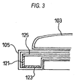
- the radiating element 121 and the auxiliary bottom board 123 are exposed flush with the surface of the lower casing 105, but while a similar positional relationship is held, they may be provided inside the lower casing 105, as shown in FIG. 3. In this case, the radiating element 121 and the auxiliary bottom board 123 are not exposed, so that the design of the communication terminal is not impaired and complicating the shape of the lower casing 105 can be prevented.
- the auxiliary bottom board 123 forms a capacitor together with the metal plate 141 and thus becomes short-circuited in a high-frequency manner. Therefore, the radiating element 121 radiates an electric field of polarization component perpendicular to the metal plate 141 by the mirror image effect.
- the lower casing 105 may be shaped so that a radiating element 153 is exposed from the peripheral portion of the parts 151, as shown in FIG. 4.
- the radiating element 153 and an auxiliary bottom board 155 are formed as separate bodies and are joined, but may be formed in one piece.
- each area of the auxiliary bottom board 123 shown in FIGS. 2 and 3 and the auxiliary bottom board 155 shown in FIG. 4 is 20 square millimeters or more as the minimum required area to short-circuit in a high-frequency manner to the metal plate 141.
- FIG. 5 is a schematic representation to schematically show the main part of a communication terminal of a second embodiment from a bottom face.
- FIG. 6 is a schematic representation to schematically show the communication terminal of the second embodiment from a side (a) and from a rear (b). Parts identical with those in FIGS. 1 and 2 (first embodiment) are denoted by the same reference numerals in FIGS. 5 and 6.
- the communication terminal of the second embodiment is provided with a board 125, metal fittings 201, a radiating element 203, and an auxiliary bottom board 205 inside a lower casing 105, as shown in FIGS. 5 and 6.
- the radiating element 203 and the auxiliary bottom board 205 are formed in one piece.
- the metal fittings 201 are fittings for fixing parts 207 of a connector, a jack, etc., to the board 125 and are electrically connected to GND of the board 125.
- the radiating element 203 is provided with roof-type spring parts 209 to come in contact with the metal fittings 201, and the radiating element 203 and the auxiliary bottom board 205 are electrically connected to the GND of the board 125 through the metal fittings 201.
- the metal fittings 201, the radiating element 203, and the auxiliary bottom board 205 may be formed in one piece.
- the radiating element 203 and the auxiliary bottom board 205 can be installed in a narrow space below the parts 207 and can be electrically connected to the GND of the board 125 through the metal fittings 201, so that similar advantages to those of the first embodiment can be provided. That is, the current components perpendicular to a metal plate strengthen each other by the mirror image effect even in a state in which the communication terminal is placed on the metal plate and thus the high-frequency current flowing through the top of the board 125 flows into the radiating element 203 and the metal fittings 201 as an extension of the board, radiating an electric field of polarization component perpendicular to the metal plate. Thus, the antenna gain is not degraded and the reception sensitivity can be kept good.
- one metal fitting 201 a may be connected directly to the GND of the board 125 and the other metal fitting 201 b may be connected through a passive element (for example, an element having an L component) 211 to the GND of the board 125.
- the passive element 211 is thus inserted between either metal fitting 201 and the radiating element 203, whereby the electric distribution of the radiating element 203 and the metal fitting 201 can be changed.
- the resonance frequency of the radiating element 203 provided by the radiating element 203 and the metal fitting 201 can be adjusted to any desired frequency in the presence of the passive element 211. Consequently, the dipole antenna can radiate an electromagnetic wave of any desired frequency.
- the area of the auxiliary bottom board 205 is 20 square millimeters or more as the minimum required area to short-circuit in a high-frequency manner to the metal plate.
- FIG. 7 is an external view to show a state in which a rear cover of a lower casing of a communication terminal of a third embodiment is removed from the rear.
- FIG. 8 is a schematic representation to schematically show the main part of the communication terminal of the third embodiment from a side. Parts identical with those in FIGS. 1 and 2 (first embodiment) are denoted by the same reference numerals in FIGS. 7 and 8.
- the communication terminal of the third embodiment is provided with a board 301, a shield case 303 attached to the rear of the board 301, a radiating element 305, and an auxiliary bottom board 307 inside a lower casing 105, as shown in FIGS. 7 and 8.
- the radiating element 305 and the auxiliary bottom board 307 are formed in one piece on the rear of the lower casing 105 of the board 301.
- the radiating element 305 is formed in such a manner that a part of the auxiliary bottom board 307 is lifted up from the rear and is pressed against the shield case 303. Therefore, the shield case 303 and the radiating element 305 are electrically connected in a state in which the board 301 with the shield case 303, the radiating element 305, and the auxiliary bottom board 307 are installed inside the lower casing 105.
- the auxiliary bottom board 307 forms a capacitor together with the metal plate and thus becomes short-circuited in a high-frequency manner. Therefore, the high-frequency current flowing through the top of the board 301 flows into the radiating element 305 as an extension of the board 301 by the mirror image effect, and the radiating element 305 radiates an electric field of polarization component perpendicular to the metal plate.
- the essential radiation of the antenna 107 is weakened as the communication terminal is placed on the metal plate, but the radiating element 305 contributes to the radiation and thus the antenna gain is not degraded and the reception sensitivity can be kept good.
- the resonance frequency of the radiating element 305 can be set to any desired frequency, so that the radiating element 305 can radiate an electromagnetic wave of any desired frequency.
- the radiating element 305 and the auxiliary bottom board 307 can be formed. Therefore, in a state in which the communication terminal is placed on a metal plate with the communication terminal laid on its side, the auxiliary bottom board 305 is short-circuited to the metal plate in a high-frequency manner and the high-frequency current on the top of the board 301 flows into the radiating element 305 as an extension of the board 301, radiating an electric field of polarization component perpendicular to the metal plate.
- the contact point between the radiating element 305 and the shield case 303 is set to an appropriate position on the board 301, whereby radiation from the radiating element 305 can be accomplished at any desired frequency.
- the auxiliary bottom board 307 is provided inside the lower casing 105, but may be provided so that it is exposed flush with a rear 111 of the lower casing 105.
- the shape of the radiating element 305 is not limited to the example shown in the figure and may be any if perpendicular component with the auxiliary bottom board 307 is formed. However, preferably the area of the auxiliary bottom board 307 is 20 square millimeters or more as the minimum required area to short-circuit in a high-frequency manner to the metal plate.
- Each communication terminal described below is a folding communication machine such as a mobile telephone or a PHS including an antenna.
- the communication terminal is not limited to the folding communication machine and may be a straight type or flip type communication machine.
- FIG. 10 is VSWR characteristic drawings provided by (a) communication terminal in related art, (b) the small radio in FIG. 9, and (c) the communication terminal of the embodiment.
- VSWR Voltage Standing Wave Radio
- FIG. 10 (a) is a VSWR characteristic drawing of communication terminal in related art wherein the radiating element 121 and the auxiliary bottom board 123 are removed from the communication terminal of the first embodiment.
- FIG. 10 (b) is a VSWR characteristic drawing of the small radio shown in FIG. 9.
- FIG. 10 (c) is a VSWR characteristic drawing of the communication terminals of the first, second, and third embodiments.
- the VSWR characteristic drawing of FIG. 10 (b) shows that the VSWR value decreases a little in the band of 880 MHz to 960 MHz sandwiched between two lines in the figure.
- the VSWR characteristic drawing of FIG. 10 (c) shows that the VSWR value decreases largely in the band of 880 MHz to 960 MHz and the peak of the VSWR value exists and thus resonance as the antenna can be observed and large improvement can be understood.
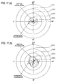
- FIG. 11 is directional patterns of horizontal polarization and vertical polarization provided by (a) communication terminal in related art and (b) the communication terminal of the embodiment.
- the directional pattern of horizontal polarization shows the directivity of the horizontal plane when the communication terminal is placed so that an antenna becomes parallel with the horizontal plane.
- the directional pattern of vertical polarization shows the directivity of the horizontal plane when the communication terminal is placed so that an antenna becomes vertical to the horizontal plane.
- the directivity of horizontal polarization is largely improved in the vertical direction to the antenna and the directivity of vertical polarization is largely improved omnidirectionally.
- a high-frequency current flows from the antenna to the board. Since a high-frequency current of an opposite phase flows through a metal plate because of the mirror image effect in a state in which the communication terminal is placed on the metal plate with the rear of the casing down, the high-frequency current flowing through the board of the communication terminal is canceled and thus the radiation of the antenna is weakened.
- the first conductor part in the state, is electrically connected to the metal plate or is short-circuited in a high-frequency manner to the metal plate and the second conductor part is connected to the GND of the board; the components perpendicular to the metal plate strengthen each other by the mirror image effect and thus the high-frequency current flowing through the top of the board flows into the second conductor part as an extension of the board, producing an electric field perpendicular to the metal plate.
- the antenna gain is not degraded and the reception sensitivity can be kept good.
- the first conductor part and the second conductor part can be installed with almost no need for changing the size or the design of the communication terminal.
Landscapes
- Engineering & Computer Science (AREA)
- Computer Networks & Wireless Communication (AREA)
- Support Of Aerials (AREA)
- Transceivers (AREA)
- Details Of Aerials (AREA)
- Telephone Set Structure (AREA)
- Aerials With Secondary Devices (AREA)
Applications Claiming Priority (3)
| Application Number | Priority Date | Filing Date | Title |
|---|---|---|---|
| JP2002324084 | 2002-11-07 | ||
| JP2002324084 | 2002-11-07 | ||
| PCT/JP2003/014223 WO2004042947A1 (fr) | 2002-11-07 | 2003-11-07 | Terminal de communications |
Publications (2)
| Publication Number | Publication Date |
|---|---|
| EP1560342A1 true EP1560342A1 (fr) | 2005-08-03 |
| EP1560342A4 EP1560342A4 (fr) | 2012-08-01 |
Family
ID=32310433
Family Applications (1)
| Application Number | Title | Priority Date | Filing Date |
|---|---|---|---|
| EP03810670A Withdrawn EP1560342A4 (fr) | 2002-11-07 | 2003-11-07 | Terminal de communications |
Country Status (7)
| Country | Link |
|---|---|
| US (1) | US7519174B2 (fr) |
| EP (1) | EP1560342A4 (fr) |
| JP (2) | JP4205670B2 (fr) |
| KR (1) | KR100931290B1 (fr) |
| CN (1) | CN1708915B (fr) |
| AU (1) | AU2003301785A1 (fr) |
| WO (1) | WO2004042947A1 (fr) |
Families Citing this family (11)
| Publication number | Priority date | Publication date | Assignee | Title |
|---|---|---|---|---|
| JP5000110B2 (ja) | 2005-08-24 | 2012-08-15 | 日本電気株式会社 | 折り畳み式携帯装置およびその筐体の製造方法 |
| US8138979B2 (en) * | 2006-02-24 | 2012-03-20 | Kyocera Corporation | Portable wireless apparatus |
| JP4146478B2 (ja) * | 2006-07-07 | 2008-09-10 | 株式会社東芝 | 無線モジュール及び携帯端末 |
| JP5121051B2 (ja) | 2007-12-26 | 2013-01-16 | パナソニック株式会社 | 無線通信端末 |
| JP2009171163A (ja) | 2008-01-15 | 2009-07-30 | Panasonic Corp | 携帯無線装置 |
| JP4197734B2 (ja) * | 2008-05-26 | 2008-12-17 | 株式会社東芝 | 無線モジュール |
| JP2010141723A (ja) * | 2008-12-12 | 2010-06-24 | Panasonic Corp | 携帯無線機 |
| WO2010150543A1 (fr) * | 2009-06-23 | 2010-12-29 | パナソニック株式会社 | Terminal portatif sans fil |
| KR20110003854A (ko) * | 2009-07-06 | 2011-01-13 | 엘지전자 주식회사 | 이동 단말기 |
| JP6224617B2 (ja) * | 2012-11-28 | 2017-11-01 | シャープ株式会社 | 構造体 |
| JP7535398B2 (ja) * | 2020-07-06 | 2024-08-16 | 株式会社Soken | アンテナ搭載システム |
Family Cites Families (28)
| Publication number | Priority date | Publication date | Assignee | Title |
|---|---|---|---|---|
| JPS62161410A (ja) | 1986-01-09 | 1987-07-17 | Ishikawajima Harima Heavy Ind Co Ltd | 圧延機 |
| JPH06338816A (ja) * | 1993-05-28 | 1994-12-06 | Sony Corp | 携帯無線機 |
| JP3493808B2 (ja) * | 1995-05-23 | 2004-02-03 | ソニー株式会社 | 電磁波遮蔽装置 |
| JPH0918220A (ja) * | 1995-06-27 | 1997-01-17 | Sharp Corp | 小型無線機 |
| JPH0983241A (ja) * | 1995-09-13 | 1997-03-28 | Toshiba Corp | 半導体装置 |
| JP3204618B2 (ja) | 1996-10-14 | 2001-09-04 | 松下電器産業株式会社 | 小形無線機 |
| JPH10256819A (ja) | 1997-03-12 | 1998-09-25 | Toshiba Corp | 無線機及び無線システム |
| JP2000049520A (ja) * | 1998-05-26 | 2000-02-18 | Matsushita Electric Ind Co Ltd | アンテナ装置 |
| JP2000315905A (ja) * | 1999-04-30 | 2000-11-14 | Matsushita Electric Ind Co Ltd | アンテナ構造及びカード型無線端末 |
| SE517564C2 (sv) * | 1999-11-17 | 2002-06-18 | Allgon Ab | Antennanordning för en bärbar radiokommunikationsanordning, bärbar radiokommunikationsanordning med sådan antennanordning och metod för att driva nämnda radiokommunikationsanordning |
| JP2001217641A (ja) | 2000-02-04 | 2001-08-10 | Harada Ind Co Ltd | 接地型アンテナ装置 |
| JP3739641B2 (ja) * | 2000-04-19 | 2006-01-25 | 富士通株式会社 | 折りたたみ型携帯機 |
| JP2002094311A (ja) | 2000-07-14 | 2002-03-29 | Sony Corp | アンテナ装置及び携帯型無線端末 |
| US6266019B1 (en) * | 2000-07-21 | 2001-07-24 | Ericsson Inc. | System for increasing antenna efficiency |
| JP2002050914A (ja) * | 2000-07-31 | 2002-02-15 | Matsushita Electric Ind Co Ltd | アンテナ装置及びこれを搭載した携帯無線機 |
| JP2002064314A (ja) | 2000-08-15 | 2002-02-28 | Sony Corp | 無線通信装置 |
| JP4071452B2 (ja) * | 2001-04-13 | 2008-04-02 | 松下電器産業株式会社 | 携帯無線機 |
| JP3671859B2 (ja) * | 2001-04-27 | 2005-07-13 | 三菱電機株式会社 | 携帯無線機 |
| JP2002353719A (ja) | 2001-05-30 | 2002-12-06 | Sony Corp | Sar低減装置および無線通信装置 |
| JP3502071B2 (ja) | 2001-08-08 | 2004-03-02 | 松下電器産業株式会社 | 無線機用アンテナ装置 |
| JP2003069441A (ja) * | 2001-08-23 | 2003-03-07 | Nec Saitama Ltd | 折り畳み型携帯無線機 |
| US7136681B2 (en) * | 2001-10-31 | 2006-11-14 | Telefonaktiebolaget Lm Ericsson (Publ) | Electrically conductive carrier and patterning for controlling current distribution in a wireless communications device |
| JP2003283238A (ja) | 2002-01-18 | 2003-10-03 | Matsushita Electric Ind Co Ltd | アンテナ装置、通信装置、およびアンテナ装置設計方法 |
| DE10204877A1 (de) | 2002-02-06 | 2003-08-14 | Siemens Ag | Funkkommunikationsgerät sowie Leiterplatine mit mindestens einem stromleitfähigen Korrekturelement |
| JP2003338769A (ja) * | 2002-05-22 | 2003-11-28 | Nec Access Technica Ltd | 携帯無線端末装置 |
| JP2003347815A (ja) | 2002-05-23 | 2003-12-05 | Nec Corp | 携帯無線機 |
| JP2004032808A (ja) | 2003-08-04 | 2004-01-29 | Matsushita Electric Ind Co Ltd | 無線機用アンテナ装置 |
| JP2005286895A (ja) | 2004-03-30 | 2005-10-13 | Nec Access Technica Ltd | アンテナ装置および携帯無線装置 |
-
2003
- 2003-11-07 JP JP2004549647A patent/JP4205670B2/ja not_active Expired - Fee Related
- 2003-11-07 AU AU2003301785A patent/AU2003301785A1/en not_active Abandoned
- 2003-11-07 CN CN2003801022741A patent/CN1708915B/zh not_active Expired - Fee Related
- 2003-11-07 EP EP03810670A patent/EP1560342A4/fr not_active Withdrawn
- 2003-11-07 KR KR1020057007927A patent/KR100931290B1/ko not_active Expired - Fee Related
- 2003-11-07 US US10/534,153 patent/US7519174B2/en not_active Expired - Fee Related
- 2003-11-07 WO PCT/JP2003/014223 patent/WO2004042947A1/fr not_active Ceased
-
2007
- 2007-08-07 JP JP2007205220A patent/JP2007329962A/ja active Pending
Also Published As
| Publication number | Publication date |
|---|---|
| JP2007329962A (ja) | 2007-12-20 |
| CN1708915A (zh) | 2005-12-14 |
| AU2003301785A1 (en) | 2004-06-07 |
| US7519174B2 (en) | 2009-04-14 |
| CN1708915B (zh) | 2010-05-12 |
| JPWO2004042947A1 (ja) | 2006-03-09 |
| KR20050084665A (ko) | 2005-08-26 |
| US20060017625A1 (en) | 2006-01-26 |
| KR100931290B1 (ko) | 2009-12-11 |
| WO2004042947A1 (fr) | 2004-05-21 |
| JP4205670B2 (ja) | 2009-01-07 |
| EP1560342A4 (fr) | 2012-08-01 |
Similar Documents
| Publication | Publication Date | Title |
|---|---|---|
| US8203493B2 (en) | Portable wireless device | |
| JP4358084B2 (ja) | 折畳式携帯無線機 | |
| JP2007329962A (ja) | 通信端末 | |
| US6963310B2 (en) | Mobile phone antenna | |
| US6535170B2 (en) | Dual band built-in antenna device and mobile wireless terminal equipped therewith | |
| US6897814B2 (en) | Mobile radio | |
| CN103081220B (zh) | 天线装置及无线通信机 | |
| JP2008305168A (ja) | 電子機器及びその製造方法 | |
| US7642969B2 (en) | Mobile communication terminal incorporating internal antenna | |
| JP4095072B2 (ja) | 携帯型通信機器のアンテナ | |
| US6990363B2 (en) | Wireless communication device with an improved antenna structure | |
| JP2004242165A (ja) | 携帯無線機 | |
| US20110156960A1 (en) | Antenna module | |
| JP4400427B2 (ja) | 携帯無線機 | |
| JP4436197B2 (ja) | 携帯無線機 | |
| KR20060007590A (ko) | 이동 통신 단말기의 내장형 안테나 | |
| JPH08222928A (ja) | アンテナ装置 | |
| CN119029543A (zh) | 天线组件及可折叠的电子设备 | |
| JP2004363789A (ja) | 逆fアンテナ | |
| JP2002076737A (ja) | 携帯通信機器のアンテナ装置 | |
| JPH10107536A (ja) | 表面実装型アンテナ |
Legal Events
| Date | Code | Title | Description |
|---|---|---|---|
| PUAI | Public reference made under article 153(3) epc to a published international application that has entered the european phase |
Free format text: ORIGINAL CODE: 0009012 |
|
| 17P | Request for examination filed |
Effective date: 20050427 |
|
| AK | Designated contracting states |
Kind code of ref document: A1 Designated state(s): AT BE BG CH CY CZ DE DK EE ES FI FR GB GR HU IE IT LI LU MC NL PT RO SE SI SK TR |
|
| AX | Request for extension of the european patent |
Extension state: AL LT LV MK |
|
| DAX | Request for extension of the european patent (deleted) | ||
| RBV | Designated contracting states (corrected) |
Designated state(s): DE FR GB IT |
|
| RAP1 | Party data changed (applicant data changed or rights of an application transferred) |
Owner name: PANASONIC CORPORATION |
|
| A4 | Supplementary search report drawn up and despatched |
Effective date: 20120703 |
|
| RIC1 | Information provided on ipc code assigned before grant |
Ipc: H04M 1/02 20060101ALI20120627BHEP Ipc: H01Q 1/48 20060101ALN20120627BHEP Ipc: H01Q 1/24 20060101AFI20120627BHEP |
|
| STAA | Information on the status of an ep patent application or granted ep patent |
Free format text: STATUS: THE APPLICATION HAS BEEN WITHDRAWN |
|
| 18W | Application withdrawn |
Effective date: 20130218 |