EP1573802B1 - Herstellung von hohlräumen in einer siliziumscheibe - Google Patents
Herstellung von hohlräumen in einer siliziumscheibe Download PDFInfo
- Publication number
- EP1573802B1 EP1573802B1 EP03799651A EP03799651A EP1573802B1 EP 1573802 B1 EP1573802 B1 EP 1573802B1 EP 03799651 A EP03799651 A EP 03799651A EP 03799651 A EP03799651 A EP 03799651A EP 1573802 B1 EP1573802 B1 EP 1573802B1
- Authority
- EP
- European Patent Office
- Prior art keywords
- zone
- insulating layer
- implanted
- atoms
- silicon
- Prior art date
- Legal status (The legal status is an assumption and is not a legal conclusion. Google has not performed a legal analysis and makes no representation as to the accuracy of the status listed.)
- Expired - Lifetime
Links
Images


Classifications
-
- B—PERFORMING OPERATIONS; TRANSPORTING
- B81—MICROSTRUCTURAL TECHNOLOGY
- B81C—PROCESSES OR APPARATUS SPECIALLY ADAPTED FOR THE MANUFACTURE OR TREATMENT OF MICROSTRUCTURAL DEVICES OR SYSTEMS
- B81C1/00—Manufacture or treatment of devices or systems in or on a substrate
- B81C1/00436—Shaping materials, i.e. techniques for structuring the substrate or the layers on the substrate
- B81C1/005—Bulk micromachining
- B81C1/00507—Formation of buried layers by techniques other than deposition, e.g. by deep implantation of elements
-
- H—ELECTRICITY
- H10—SEMICONDUCTOR DEVICES; ELECTRIC SOLID-STATE DEVICES NOT OTHERWISE PROVIDED FOR
- H10P—GENERIC PROCESSES OR APPARATUS FOR THE MANUFACTURE OR TREATMENT OF DEVICES COVERED BY CLASS H10
- H10P30/00—Ion implantation into wafers, substrates or parts of devices
- H10P30/20—Ion implantation into wafers, substrates or parts of devices into semiconductor materials, e.g. for doping
- H10P30/202—Ion implantation into wafers, substrates or parts of devices into semiconductor materials, e.g. for doping characterised by the semiconductor materials
- H10P30/204—Ion implantation into wafers, substrates or parts of devices into semiconductor materials, e.g. for doping characterised by the semiconductor materials into Group IV semiconductors
-
- H—ELECTRICITY
- H10—SEMICONDUCTOR DEVICES; ELECTRIC SOLID-STATE DEVICES NOT OTHERWISE PROVIDED FOR
- H10P—GENERIC PROCESSES OR APPARATUS FOR THE MANUFACTURE OR TREATMENT OF DEVICES COVERED BY CLASS H10
- H10P30/00—Ion implantation into wafers, substrates or parts of devices
- H10P30/20—Ion implantation into wafers, substrates or parts of devices into semiconductor materials, e.g. for doping
- H10P30/208—Ion implantation into wafers, substrates or parts of devices into semiconductor materials, e.g. for doping of electrically inactive species
-
- H—ELECTRICITY
- H10—SEMICONDUCTOR DEVICES; ELECTRIC SOLID-STATE DEVICES NOT OTHERWISE PROVIDED FOR
- H10P—GENERIC PROCESSES OR APPARATUS FOR THE MANUFACTURE OR TREATMENT OF DEVICES COVERED BY CLASS H10
- H10P90/00—Preparation of wafers not covered by a single main group of this subclass, e.g. wafer reinforcement
- H10P90/19—Preparing inhomogeneous wafers
- H10P90/1904—Preparing vertically inhomogeneous wafers
- H10P90/1906—Preparing SOI wafers
-
- H—ELECTRICITY
- H10—SEMICONDUCTOR DEVICES; ELECTRIC SOLID-STATE DEVICES NOT OTHERWISE PROVIDED FOR
- H10W—GENERIC PACKAGES, INTERCONNECTIONS, CONNECTORS OR OTHER CONSTRUCTIONAL DETAILS OF DEVICES COVERED BY CLASS H10
- H10W10/00—Isolation regions in semiconductor bodies between components of integrated devices
- H10W10/01—Manufacture or treatment
- H10W10/021—Manufacture or treatment of air gaps
-
- H—ELECTRICITY
- H10—SEMICONDUCTOR DEVICES; ELECTRIC SOLID-STATE DEVICES NOT OTHERWISE PROVIDED FOR
- H10W—GENERIC PACKAGES, INTERCONNECTIONS, CONNECTORS OR OTHER CONSTRUCTIONAL DETAILS OF DEVICES COVERED BY CLASS H10
- H10W10/00—Isolation regions in semiconductor bodies between components of integrated devices
- H10W10/10—Isolation regions comprising dielectric materials
- H10W10/181—Semiconductor-on-insulator [SOI] isolation regions, e.g. buried oxide regions of SOI wafers
-
- H—ELECTRICITY
- H10—SEMICONDUCTOR DEVICES; ELECTRIC SOLID-STATE DEVICES NOT OTHERWISE PROVIDED FOR
- H10W—GENERIC PACKAGES, INTERCONNECTIONS, CONNECTORS OR OTHER CONSTRUCTIONAL DETAILS OF DEVICES COVERED BY CLASS H10
- H10W10/00—Isolation regions in semiconductor bodies between components of integrated devices
- H10W10/20—Air gaps
-
- H—ELECTRICITY
- H10—SEMICONDUCTOR DEVICES; ELECTRIC SOLID-STATE DEVICES NOT OTHERWISE PROVIDED FOR
- H10P—GENERIC PROCESSES OR APPARATUS FOR THE MANUFACTURE OR TREATMENT OF DEVICES COVERED BY CLASS H10
- H10P30/00—Ion implantation into wafers, substrates or parts of devices
- H10P30/20—Ion implantation into wafers, substrates or parts of devices into semiconductor materials, e.g. for doping
- H10P30/22—Ion implantation into wafers, substrates or parts of devices into semiconductor materials, e.g. for doping using masks
Definitions
- the invention relates to the field of the production of components or semiconductor elements, in particular from components or elements of the SOI type (abbreviation of Silicon on Insulator or Silicon on Insulator).
- the document FR2700065 describes a method of manufacturing a silicon on insulator structure comprising steps of implantation of oxgen and boron ions.
- An SOI structure comprises a silicon layer, in which the components themselves, and in which is made a buried layer of insulation, for example silicon dioxide. The latter constitutes an isolation vis-à-vis the parasitic currents and charges from ionized particles. It also allows good insulation of neighboring components made in the same silicon layer, and in particular a significant decrease in parasitic capacitances between such neighboring components. It rests itself on a silicon substrate, which plays the role of mechanical support.
- a substrate made of silicon or semiconductor material it is desired to make one or more cavities in a substrate made of silicon or semiconductor material.
- Cavity means a hollow volume overhung by a layer of semiconductor material.
- the invention firstly relates to a method for producing a semiconductor structure according to claim 1.
- Such a structure can be realized from an SOI structure.
- the etching rate of the insulating layer, after it has undergone atomic implantation, is greater than the etching rate of a virgin insulator.
- the invention thus makes it possible to define regions or zones of the insulating layer having different etching rates.
- the atomic implantation can be carried out through the entire thickness of the insulating layer, or through only a part of this layer, then forming an upper part of insulation traversed by the ions and a lower part of insulator. crossed by the ions.
- At least one hole may be formed in the surface layer of silicum, opening into the insulating layer, for example within an area traversed by the atomic implantation, or at the limit of an area crossed by the atomic implantation and a zone not traversed by the atomic implantation, or in a zone of concave, convex or polygonal shape, and traversed by the atomic implantation.
- the insulating material may for example be chosen from silicon dioxide (SiO 2), silicon nitride (Si 3 N 4), diamond, sapphire, hafnium oxide (HfO 2), zirconium oxide (ZrO 2), alumina (Al 2 O 3), lanthanum oxide (La 2 O 3), ytterbium oxide (Y 2 O 3).
- the etching step is performed using an acid, but can also be a dry etching step or wet.
- the invention also relates to a semiconductor structure according to claim 14.
- the atomic implantation zone according to claim 14 may, for example, have in a plane parallel to the mean plane of said buried insulating layer a concave or convex shape or be of polygonal shape. Any other form can be realized.
- a cavity may be formed in the insulation layer.
- at least a portion of said cavity is formed in a portion of the insulation layer traversed by the ions of the atomic implantation.
- This cavity may for example be cylindrical or semi-cylindrical.
- Other shapes can be made such as shapes having, in a plane parallel to the mean plane of the insulation layer, an at least partially elliptical section and / or at least partially polygonal.
- said cavity comprises a first zone having a first diameter, or a first maximum or characteristic dimension, and a second zone, having a second diameter, or a second maximum or characteristic dimension, different from the first one.
- These first and second zones may be located at different average depths in the insulation layer.
- These two zones may be located at the same depth in the insulation layer, or at different average depths in the insulation layer.
- the figure 1 schematically represents an SOI substrate in which an atomic implantation has been performed.
- Such an SOI structure comprises a layer 2 of silicon, preferably monocrystalline, in which the components themselves can be made, and in which is formed a buried layer 4 of an insulator, for example silicon oxide.
- This insulating layer 4 constitutes an isolation vis-à-vis the parasitic currents and charges from ionized particles. It also allows good insulation of neighboring components made in the same silicon layer 2, and in particular a significant decrease in stray capacitances between such neighboring components. It rests itself on a substrate 6 made of a material chosen from semiconductor materials, for example silicon, which acts as a mechanical support.
- the surface layer of silicon has a thickness of about 10 to 500 nm or 1000 nm or 3000 nm, while the insulation layer has for example a thickness of the order of a few hundred nm, for example included between 100 nm or 200 nm and 400 nm or 500 nm.
- These thicknesses, and in particular that of the insulating layer, may vary.
- an atomic implantation of this structure is carried out by atomic or ionic species, for example hydrogen or helium species, such as H + or H 2 + or He 2+ , at a depth located at least in the layer. insulation, for example or below the insulation layer.
- atomic or ionic species for example hydrogen or helium species, such as H + or H 2 + or He 2+ .
- insulation for example or below the insulation layer.
- the plane 18 represents the average plane in which the ions have been implanted: all the material situated above this plane has been traversed by the ion flux of the atomic implantation.
- the curve 19, centered on this plane, represents the average distribution of the ions in the substrate 6.
- the plane 18 is located in the substrate 6, but it could also be in the layer 4, in which case only a portion insulation 4 would have been crossed by the path of the ions.
- the etching of the buried insulator can be carried out, for example using an acid such as hydrofluoric acid HF introduced through a hole 22 (shown in broken lines on the figure 1 ) opening into the insulating layer.
- an acid such as hydrofluoric acid HF introduced through a hole 22 (shown in broken lines on the figure 1 ) opening into the insulating layer.
- Other etching processes can be used, with the same advantages, such as for example dry etching or wet etching with fluorinated compounds.
- FIGS. 2A to 2C represent different steps of a method according to the invention.
- an implantation mask 32 defining the zone to be implanted is deposited ( Figure 2A ).
- the depth of the insulator or the buried oxide 36 defines that of the cavity to be created.
- Reference 34 designates the superficial silicon layer.
- the implantation of atomic species is carried out on the plate, through the opening of the mask ( Figure 2B ), the rest of the mask protecting the SOI of these species.
- the implantation energy can be chosen to have created a high density of implanted species either in the buried insulator or oxide layer, or at a depth, measured from the surface of the layer surface silicum 34, located beyond this buried insulator or oxide.
- a through hole 40 is produced using conventional microelectronic etching techniques ( Figure 2C ).
- the figure 3A represents a top view of an SOI substrate in which a process such as that described above has been implemented.
- the implanted and engraved areas are in gray
- the implanted and ungraved areas are in hatched lines
- the non-implanted areas are in white.
- the reference 40 designates the implanted zone of this substrate, the non-implanted zone being designated by the reference 41.
- the opening hole made in the substrate is designated by the reference 42 and is located in the heart of the implanted zone. 40.
- the etching is performed progressively in the implanted area and more quickly than in a non-implanted area.
- the reference 44 designates the cylinder, or the etched area, after a duration ⁇ T
- the reference 46 the etched area after a duration of 2 ⁇ T
- the area 48 the etched area after a duration of 3 ⁇ T.
- the figure 3B corresponds to the case of a through hole created at the boundary 57 of the implanted zone 50 and the non-implanted zone 51, both located in the insulating or silicon dioxide layer.
- Etching progresses both in these two areas, 50, 51.
- the etching rates in these two areas are however different from each other.
- the engraved area 54 in the implanted area 50 is, after a duration ⁇ T, wider than the corresponding area 64 in the non-implanted region 51.
- the etched region 56 is wider than the etched region 66 and, after a duration 3 ⁇ T, the region 58 is wider than the region 68.
- FIG 3C corresponds to the case of a through hole created in the center of a concave shaped implant area 60 located in the zone 59 otherwise not implanted, thereby creating a cavity 69 of square or substantially square shape.
- references 65, 67, 69 denote the cavities obtained after respective durations of ⁇ T, 2 ⁇ T, and 3 ⁇ T.
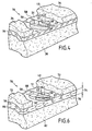
- the figure 4 represents in perspective the case of the figure 3B , references 34, 36, 38 having the same meaning as on the Figure 2B .
- the two half-cylinders 58 and 68 pass through the insulating layer 36, in a direction perpendicular to the plane of this layer and to the plane of the silicon surface layer 34.
- the figure 5 represents an SOI structure 70 in which the silicon surface layer 72 and the insulator or oxide layer 74 have been treated by the ion flux only to a depth identified by the plane 76 (zone or plane of impantation of ions).
- the insulator or silicon dioxide layer is divided into an upper portion 78 which has been traversed by the flow of ions and a portion 80 not traversed by the flow of ions.
- the etching speed will then be different in these two zones, which makes it possible to produce etched patterns having section or diameter variations along an axis perpendicular to plane 76 or to the plane of layer 72 and layer 78.
- the figure 6 represents in perspective the result of an etching of the insulating layer 74.
- the etched area 88 is similar to the etched area 58 of the figure 4 , but on a reduced thickness with respect to the total thickness of the layer 36.
- two portions of insulation located at two distinct depths, are also etched (next to each of the etched areas 88 and 90), but at the same speed because they are both in a non-implanted region. They both have the same diameter or the same dimension and they constitute the engraved area 98.
- the invention makes it possible to define in an insulating layer such as the layer 4 of the figure 1 regions for which the etching rates of this layer are different from one region to another.
- the insulating layer then has at least a first and a second region, respectively having first and second etch rates which are different from each other.
- the point or the place where the etching begins may be located in a non-implanted zone, the etching then propagating in a zone implanted at a speed different from the etching in the non-implanted area.
- the combination of the various embodiments mentioned above makes it possible to produce etched areas having different dimensions in two or three directions of space. So, in the case of the figure 6 , the diameter or the largest dimension or the characteristic dimension in each portion or etched area, or the section of this portion or etched area, varies both in the plane of the layer 74, and in a direction perpendicular to this plane.
- One and / or the other of these zones may be of square section (as on the figure 3C ) or be cylindrical ( figure 3A ) or semi-cylindrical ( figure 3B ). Other forms can still be made, depending on the shape of the mask initially chosen for the implantation and the point or place where the etching begins in the implanted region or outside thereof.
- a cavity having, in a parallel plane or mean plane of the insulating layer, an elliptical or polygonal section, or a part that is elliptical and partly polygonal.
- the atomic implantation zone may in fact be of totally arbitrary, convex, concave shape or any other form. This The shape of the atomic implantation zone is related to the final shape of the desired cavity.
- electronic components for example transistors, may then be made in the silicon surface layer 2, 34, 72.
- the zone etched in the insulating layer makes it possible, for example, to make a conductive portion of such a component.
- the SiO 2 material can be used as an insulator of an SOI structure.
- the invention however also applies to other insulating materials, such as for example Si3N4, SiGe, diamond, or sapphire. It also applies to any material with a high K-value, such as those described in MRS Bulletin, March 2002, Vol. 27, No.3, in an article entitled "Alternative Gate Dielectrics for Microelectronics” ; such materials are, for example, Haffnium oxide (HfO 2), or zirconium oxide (ZrO 2), alumina (Al 2 O 3), or Y 2 O 3 (ytterbium oxide).
- HfO 2 Haffnium oxide
- ZrO 2 zirconium oxide
- Al 2 O 3 alumina
- Y 2 O 3 ytterbium oxide
Landscapes
- Engineering & Computer Science (AREA)
- Manufacturing & Machinery (AREA)
- Microelectronics & Electronic Packaging (AREA)
- Element Separation (AREA)
- Thin Film Transistor (AREA)
- Silicon Compounds (AREA)
- Recrystallisation Techniques (AREA)
- Crystals, And After-Treatments Of Crystals (AREA)
Claims (20)
- Verfahren zum Ausbilden einer Halbleiterstruktur mit einer Oberflächenschicht aus Silizium (2, 34, 72), einer verdeckten Isolatorschicht (4, 36, 74) und einem Substrat (6, 38, 82), dadurch gekennzeichnet, daß das Verfahren die folgenden Schritte umfaßt:- einen Schritt zur Atomimplantation der Halbleiterstruktur, wobei das Implantieren über einen bestimmten Bereich der Struktur und in einer wenigstens bis zu der Isolatorschicht reichenden Tiefe erfolgt, um Regionen der Isolatorschicht mit unterschiedlichen Ätzgeschwindigkeiten zu definieren, und- einen Schritt selektiven Ätzens der von der Atomimplantation durchzogenen Isolatorschicht, so daß eine Vertiefung in der Isolatorschicht ausgebildet wird, die sich unter der Oberflächenschicht aus Silizium erstreckt.
- Verfahren nach Anspruch 1, wobei die Atomimplantation durch die gesamte Dicke der Isolatorschicht hindurch erfolgt.
- Verfahren nach Anspruch 1, wobei die Atomimplantation lediglich durch einen Teil der Dicke der Isolatorschicht hindurch erfolgt.
- Verfahren nach einem der Ansprüche 1 bis 3, wobei der Implantationsschritt ein Schritt zur Implantation von Wasserstoffionen oder Heliumionen ist.
- Verfahren nach einem der Ansprüche 1 bis 4, mit einem Schritt zur Ausbildung wenigstens eines Lochs (40) in der Oberflächenschicht aus Silizium, das in die Isolatorschicht mündet.
- Verfahren nach Anspruch 5, wobei das Loch in einen von der Atomimplantation durchzogenen Bereich (40) mündet.
- Verfahren nach Anspruch 5, wobei das Loch an der Grenze zwischen einem von der Atomimplantation durchzogenen Bereich (50) und einem von der Atomimplantation nicht durchzogenen Bereich (51) ausmündet.
- Verfahren nach Anspruch 5 oder 6, wobei das Loch in einen von der Atomimplantation durchzogenen Bereich (60) konkaver oder konvexer Form mündet.
- Verfahren nach Anspruch 5 oder 6, wobei das Loch in einen von der Implantation durchzogenen Bereich polygonaler Form mündet.
- Verfahren nach Anspruch 5, wobei das Loch in einen von der Atomimplantation nicht durchzogenen Bereich mündet.
- Verfahren nach einem der Ansprüche 1 bis 10, wobei das Isolationsmaterial aus Siliziumdioxid (SiO2), Siliziumnitrid (Si3N4), Diamant, Saphir, Hafniumoxid (HfO2), Zirkoniumoxid (ZrO2), Aluminiumoxid (Al2O3), Lanthanoxid (La2O3), Ytterbiumoxid (Y2O3) ausgewählt ist.
- Verfahren nach einem der Ansprüche 1 bis 11, wobei der Ätzschritt mit Hilfe einer Säure durchgeführt wird.
- Verfahren nach einem der Ansprüche 1 bis 12, wobei der Ätzschritt ein Trocken- oder Naßätzschritt ist.
- Halbleiterstruktur, die in einem Siliziumsubstrat folgendes umfaßt:- eine Oberflächenschicht aus Silizium (2, 34, 72),- eine verdeckte Isolationsschicht (4, 36, 78) aus einem unter der Oberflächenschicht aus Silizium gebildeten Isolationsmaterial,
gekennzeichnet durch:- einen Atomimplantationsbereich (18), der in der Isolationsschicht oder unter dieser Isolationsschicht ausgebildet ist, und- eine Vertiefung (50), die wenigstens in einem Abschnitt des in der Isolatorschicht ausgebildeten Atomimplantationsbereichs gebildet ist und sich seitlich unter der Oberflächenschicht aus Silizium erstreckt. - Halbleiterstruktur nach Anspruch 14, wobei der Atomimplantationsbereich in einer zur Mittelebene der verdeckten Isolationsschicht parallelen Ebene eine konkave oder konvexe oder polygonale Form aufweist.
- Halbleiterstruktur nach Anspruch 15, wobei ein Teil der Vertiefung in einem von den lonen der Atomimplantation nicht durchquerten Abschnitt der Isolatorschicht gebildet ist.
- Halbleiterstruktur nach Anspruch 15 oder 16, wobei die Vertiefung zylinderförmig oder halbzylinderförmig ist oder einen quadratischen Querschnitt aufweist.
- Halbleiterstruktur nach einem der Ansprüche 15 bis 17, wobei die Vertiefung in einer zur Mittelebene der Isolatorschicht parallelen Ebene einen elliptischen oder polygonalen oder teilweise elliptischen und teilweise polygonalen Querschnitt aufweist.
- Halbleiterstruktur nach einem der Ansprüche 15 bis 18, wobei die Vertiefung einen ersten Bereich (58, 88) mit einem ersten Durchmesser, oder einer maximalen oder charakteristischen ersten Abmessung, sowie einen zweiten Bereich (68, 90, 98) mit einem zweiten Durchmesser, oder einer maximalen oder charakteristischen zweiten Abmessung aufweist, der bzw. die von dem ersten bzw. der ersten abweicht.
- Halbleiterstruktur nach Anspruch 19, wobei der erste und der zweite Bereich in unterschiedlichen durchschnittlichen Tiefen in der Isolatorschicht gelegen sind.
Applications Claiming Priority (5)
| Application Number | Priority Date | Filing Date | Title |
|---|---|---|---|
| FR0216409A FR2849269B1 (fr) | 2002-12-20 | 2002-12-20 | Procede de realisation de cavites dans une plaque de silicium |
| FR0216409 | 2002-12-20 | ||
| US44812403P | 2003-02-20 | 2003-02-20 | |
| US448124P | 2003-02-20 | ||
| PCT/FR2003/003820 WO2004059725A1 (fr) | 2002-12-20 | 2003-12-19 | Procede de realisation de cavites dans une plaque de silicium |
Publications (2)
| Publication Number | Publication Date |
|---|---|
| EP1573802A1 EP1573802A1 (de) | 2005-09-14 |
| EP1573802B1 true EP1573802B1 (de) | 2008-11-26 |
Family
ID=32683899
Family Applications (1)
| Application Number | Title | Priority Date | Filing Date |
|---|---|---|---|
| EP03799651A Expired - Lifetime EP1573802B1 (de) | 2002-12-20 | 2003-12-19 | Herstellung von hohlräumen in einer siliziumscheibe |
Country Status (5)
| Country | Link |
|---|---|
| EP (1) | EP1573802B1 (de) |
| AT (1) | ATE415703T1 (de) |
| AU (1) | AU2003299368A1 (de) |
| DE (1) | DE60324960D1 (de) |
| WO (1) | WO2004059725A1 (de) |
Families Citing this family (5)
| Publication number | Priority date | Publication date | Assignee | Title |
|---|---|---|---|---|
| WO2005083775A1 (en) * | 2004-02-19 | 2005-09-09 | International Business Machines Corporation | FORMATION OF PATTERNED SILICON-ON-INSULATOR (SOI)/SILICON-ON-NOTHING (SON) COMPOSITE STRUCTURE BY POROUS Si ENGINEERING |
| FR2875947B1 (fr) | 2004-09-30 | 2007-09-07 | Tracit Technologies | Nouvelle structure pour microelectronique et microsysteme et procede de realisation |
| FR2876220B1 (fr) | 2004-10-06 | 2007-09-28 | Commissariat Energie Atomique | Procede d'elaboration de structures empilees mixtes, a zones isolantes diverses et/ou zones de conduction electrique verticale localisees. |
| FR2897982B1 (fr) | 2006-02-27 | 2008-07-11 | Tracit Technologies Sa | Procede de fabrication des structures de type partiellement soi, comportant des zones reliant une couche superficielle et un substrat |
| FR3000601B1 (fr) * | 2012-12-28 | 2016-12-09 | Commissariat Energie Atomique | Procede de formation des espaceurs d'une grille d'un transistor |
Family Cites Families (6)
| Publication number | Priority date | Publication date | Assignee | Title |
|---|---|---|---|---|
| US4956314A (en) * | 1989-05-30 | 1990-09-11 | Motorola, Inc. | Differential etching of silicon nitride |
| JPH06132262A (ja) * | 1992-10-22 | 1994-05-13 | Hitachi Ltd | 薄膜のエッチング方法 |
| FR2700065B1 (fr) * | 1992-12-28 | 1995-02-10 | Commissariat Energie Atomique | Procédé de fabrication d'accéléromètres utilisant la technologie silicium sur isolant. |
| US5976945A (en) * | 1997-11-20 | 1999-11-02 | Vanguard International Semiconductor Corporation | Method for fabricating a DRAM cell structure on an SOI wafer incorporating a two dimensional trench capacitor |
| US6335292B1 (en) * | 1999-04-15 | 2002-01-01 | Micron Technology, Inc. | Method of controlling striations and CD loss in contact oxide etch |
| FR2795554B1 (fr) * | 1999-06-28 | 2003-08-22 | France Telecom | Procede de gravure laterale par trous pour fabriquer des dis positifs semi-conducteurs |
-
2003
- 2003-12-19 AT AT03799651T patent/ATE415703T1/de not_active IP Right Cessation
- 2003-12-19 DE DE60324960T patent/DE60324960D1/de not_active Expired - Lifetime
- 2003-12-19 WO PCT/FR2003/003820 patent/WO2004059725A1/fr not_active Ceased
- 2003-12-19 EP EP03799651A patent/EP1573802B1/de not_active Expired - Lifetime
- 2003-12-19 AU AU2003299368A patent/AU2003299368A1/en not_active Abandoned
Also Published As
| Publication number | Publication date |
|---|---|
| WO2004059725A1 (fr) | 2004-07-15 |
| EP1573802A1 (de) | 2005-09-14 |
| DE60324960D1 (de) | 2009-01-08 |
| AU2003299368A1 (en) | 2004-07-22 |
| ATE415703T1 (de) | 2008-12-15 |
Similar Documents
| Publication | Publication Date | Title |
|---|---|---|
| EP3646374B1 (de) | Verfahren zur übertragung einer dünnen schicht auf ein trägersubstrat mit unterschiedlichen wärmeausdehnungskoeffizienten | |
| EP1058946B1 (de) | Verfahren zur bildung von hohlräumen in einem halbleitersubstrat, mittels atom-implantation | |
| FR2842650A1 (fr) | Procede de fabrication de substrats notamment pour l'optique, l'electronique ou l'opto-electronique | |
| EP1811560A1 (de) | Verfahren zur Herstellung eines Verbundsubstrats mit verbesserten elektrischen Eigenschaften | |
| FR2489041A1 (fr) | Procede de formation d'un evidement dans un corps semi-conducteur | |
| EP1629526A1 (de) | Substrat für verspannte systeme und verfahren des kristallwachstums auf einem solchen substrat | |
| EP1797587B1 (de) | Verfahren zur erzeugung gemischter schichtstrukturen mit mehreren isolierungszonen und/oder vertikal angeordneten elektrisch leitenden zonen | |
| WO2001009944A1 (fr) | Procede de fabrication de connexions traversantes dans un substrat et substrat equipe de telles connexions | |
| FR2849269A1 (fr) | Procede de realisation de cavites dans une plaque de silicium | |
| EP2840589B1 (de) | Verbessertes Verfahren zur Trennung zwischen einer aktiven Zone eines Substrats und dessen Rückseite oder eines Teilbereichs seiner Rückseite | |
| EP2332171B1 (de) | Verfahren zur herstellung einer halbleiterstruktur mit vergrabener bodenebene | |
| EP2095407A1 (de) | Verfahren zur bildung von mikrodrähten und/oder nanodrähten | |
| EP1573802B1 (de) | Herstellung von hohlräumen in einer siliziumscheibe | |
| FR2839199A1 (fr) | Procede de fabrication de substrats avec detachement d'un support temporaire, et substrat associe | |
| FR2888400A1 (fr) | Procede de prelevement de couche | |
| EP2612352B1 (de) | Verfahren zur herstellung einer folie, etwa einer einkristallfolie, auf einem polymersubstrat | |
| EP1631982A1 (de) | Verfahren zur herstellung einer sehr dünnen schicht durch provozierte selbstragung | |
| EP1428247B1 (de) | Herstellungsverfahren für feldeffekttransistor mit selbstjustierten horizontalen gates | |
| WO2005013338A2 (fr) | Realisation d’une structure comprenant une couche protegeant contre des traitements chimiques | |
| FR2842647A1 (fr) | Procede de transfert de couche | |
| EP4473559A1 (de) | Verfahren zur herstellung einer doppelten halbleiter-auf-isolator-struktur | |
| FR2912550A1 (fr) | Procede de fabrication d'une structure ssoi. | |
| FR2849268A1 (fr) | Procede de fabrication d'un substrat demontable | |
| EP4480001B1 (de) | Verfahren zum übertragen eines dünnfilms auf ein trägersubstrat | |
| FR3115278A1 (fr) | Procédé de transfert d’une membrane |
Legal Events
| Date | Code | Title | Description |
|---|---|---|---|
| PUAI | Public reference made under article 153(3) epc to a published international application that has entered the european phase |
Free format text: ORIGINAL CODE: 0009012 |
|
| 17P | Request for examination filed |
Effective date: 20050606 |
|
| AK | Designated contracting states |
Kind code of ref document: A1 Designated state(s): AT BE BG CH CY CZ DE DK EE ES FI FR GB GR HU IE IT LI LU MC NL PT RO SE SI SK TR |
|
| AX | Request for extension of the european patent |
Extension state: AL LT LV MK |
|
| DAX | Request for extension of the european patent (deleted) | ||
| GRAP | Despatch of communication of intention to grant a patent |
Free format text: ORIGINAL CODE: EPIDOSNIGR1 |
|
| GRAS | Grant fee paid |
Free format text: ORIGINAL CODE: EPIDOSNIGR3 |
|
| GRAA | (expected) grant |
Free format text: ORIGINAL CODE: 0009210 |
|
| AK | Designated contracting states |
Kind code of ref document: B1 Designated state(s): AT BE BG CH CY CZ DE DK EE ES FI FR GB GR HU IE IT LI LU MC NL PT RO SE SI SK TR |
|
| REG | Reference to a national code |
Ref country code: GB Ref legal event code: FG4D Free format text: NOT ENGLISH |
|
| REG | Reference to a national code |
Ref country code: CH Ref legal event code: EP |
|
| REG | Reference to a national code |
Ref country code: IE Ref legal event code: FG4D Free format text: LANGUAGE OF EP DOCUMENT: FRENCH |
|
| REF | Corresponds to: |
Ref document number: 60324960 Country of ref document: DE Date of ref document: 20090108 Kind code of ref document: P |
|
| PG25 | Lapsed in a contracting state [announced via postgrant information from national office to epo] |
Ref country code: ES Free format text: LAPSE BECAUSE OF FAILURE TO SUBMIT A TRANSLATION OF THE DESCRIPTION OR TO PAY THE FEE WITHIN THE PRESCRIBED TIME-LIMIT Effective date: 20090308 Ref country code: AT Free format text: LAPSE BECAUSE OF FAILURE TO SUBMIT A TRANSLATION OF THE DESCRIPTION OR TO PAY THE FEE WITHIN THE PRESCRIBED TIME-LIMIT Effective date: 20081126 |
|
| PG25 | Lapsed in a contracting state [announced via postgrant information from national office to epo] |
Ref country code: FI Free format text: LAPSE BECAUSE OF FAILURE TO SUBMIT A TRANSLATION OF THE DESCRIPTION OR TO PAY THE FEE WITHIN THE PRESCRIBED TIME-LIMIT Effective date: 20081126 Ref country code: SI Free format text: LAPSE BECAUSE OF FAILURE TO SUBMIT A TRANSLATION OF THE DESCRIPTION OR TO PAY THE FEE WITHIN THE PRESCRIBED TIME-LIMIT Effective date: 20081126 |
|
| BERE | Be: lapsed |
Owner name: S.O.I. TEC SILICON ON INSULATOR TECHNOLOGIES Effective date: 20081231 |
|
| REG | Reference to a national code |
Ref country code: IE Ref legal event code: FD4D |
|
| PG25 | Lapsed in a contracting state [announced via postgrant information from national office to epo] |
Ref country code: MC Free format text: LAPSE BECAUSE OF NON-PAYMENT OF DUE FEES Effective date: 20081231 Ref country code: IE Free format text: LAPSE BECAUSE OF FAILURE TO SUBMIT A TRANSLATION OF THE DESCRIPTION OR TO PAY THE FEE WITHIN THE PRESCRIBED TIME-LIMIT Effective date: 20081126 Ref country code: DK Free format text: LAPSE BECAUSE OF FAILURE TO SUBMIT A TRANSLATION OF THE DESCRIPTION OR TO PAY THE FEE WITHIN THE PRESCRIBED TIME-LIMIT Effective date: 20081126 Ref country code: RO Free format text: LAPSE BECAUSE OF FAILURE TO SUBMIT A TRANSLATION OF THE DESCRIPTION OR TO PAY THE FEE WITHIN THE PRESCRIBED TIME-LIMIT Effective date: 20081126 Ref country code: BG Free format text: LAPSE BECAUSE OF FAILURE TO SUBMIT A TRANSLATION OF THE DESCRIPTION OR TO PAY THE FEE WITHIN THE PRESCRIBED TIME-LIMIT Effective date: 20090226 Ref country code: EE Free format text: LAPSE BECAUSE OF FAILURE TO SUBMIT A TRANSLATION OF THE DESCRIPTION OR TO PAY THE FEE WITHIN THE PRESCRIBED TIME-LIMIT Effective date: 20081126 |
|
| REG | Reference to a national code |
Ref country code: CH Ref legal event code: PL |
|
| PG25 | Lapsed in a contracting state [announced via postgrant information from national office to epo] |
Ref country code: SE Free format text: LAPSE BECAUSE OF FAILURE TO SUBMIT A TRANSLATION OF THE DESCRIPTION OR TO PAY THE FEE WITHIN THE PRESCRIBED TIME-LIMIT Effective date: 20090226 Ref country code: CZ Free format text: LAPSE BECAUSE OF FAILURE TO SUBMIT A TRANSLATION OF THE DESCRIPTION OR TO PAY THE FEE WITHIN THE PRESCRIBED TIME-LIMIT Effective date: 20081126 Ref country code: PT Free format text: LAPSE BECAUSE OF FAILURE TO SUBMIT A TRANSLATION OF THE DESCRIPTION OR TO PAY THE FEE WITHIN THE PRESCRIBED TIME-LIMIT Effective date: 20090427 |
|
| PG25 | Lapsed in a contracting state [announced via postgrant information from national office to epo] |
Ref country code: BE Free format text: LAPSE BECAUSE OF NON-PAYMENT OF DUE FEES Effective date: 20081231 Ref country code: SK Free format text: LAPSE BECAUSE OF FAILURE TO SUBMIT A TRANSLATION OF THE DESCRIPTION OR TO PAY THE FEE WITHIN THE PRESCRIBED TIME-LIMIT Effective date: 20081126 |
|
| PLBE | No opposition filed within time limit |
Free format text: ORIGINAL CODE: 0009261 |
|
| STAA | Information on the status of an ep patent application or granted ep patent |
Free format text: STATUS: NO OPPOSITION FILED WITHIN TIME LIMIT |
|
| PG25 | Lapsed in a contracting state [announced via postgrant information from national office to epo] |
Ref country code: CH Free format text: LAPSE BECAUSE OF NON-PAYMENT OF DUE FEES Effective date: 20081231 Ref country code: LI Free format text: LAPSE BECAUSE OF NON-PAYMENT OF DUE FEES Effective date: 20081231 |
|
| 26N | No opposition filed |
Effective date: 20090827 |
|
| PG25 | Lapsed in a contracting state [announced via postgrant information from national office to epo] |
Ref country code: CY Free format text: LAPSE BECAUSE OF FAILURE TO SUBMIT A TRANSLATION OF THE DESCRIPTION OR TO PAY THE FEE WITHIN THE PRESCRIBED TIME-LIMIT Effective date: 20081126 Ref country code: LU Free format text: LAPSE BECAUSE OF NON-PAYMENT OF DUE FEES Effective date: 20081219 Ref country code: HU Free format text: LAPSE BECAUSE OF FAILURE TO SUBMIT A TRANSLATION OF THE DESCRIPTION OR TO PAY THE FEE WITHIN THE PRESCRIBED TIME-LIMIT Effective date: 20090527 |
|
| PG25 | Lapsed in a contracting state [announced via postgrant information from national office to epo] |
Ref country code: TR Free format text: LAPSE BECAUSE OF FAILURE TO SUBMIT A TRANSLATION OF THE DESCRIPTION OR TO PAY THE FEE WITHIN THE PRESCRIBED TIME-LIMIT Effective date: 20081126 |
|
| PG25 | Lapsed in a contracting state [announced via postgrant information from national office to epo] |
Ref country code: GR Free format text: LAPSE BECAUSE OF FAILURE TO SUBMIT A TRANSLATION OF THE DESCRIPTION OR TO PAY THE FEE WITHIN THE PRESCRIBED TIME-LIMIT Effective date: 20090227 |
|
| PGFP | Annual fee paid to national office [announced via postgrant information from national office to epo] |
Ref country code: GB Payment date: 20101201 Year of fee payment: 8 |
|
| REG | Reference to a national code |
Ref country code: DE Ref legal event code: R082 Ref document number: 60324960 Country of ref document: DE Representative=s name: CBDL PATENTANWAELTE, DE |
|
| REG | Reference to a national code |
Ref country code: FR Ref legal event code: CD Owner name: SOITEC, FR Effective date: 20120907 |
|
| REG | Reference to a national code |
Ref country code: DE Ref legal event code: R081 Ref document number: 60324960 Country of ref document: DE Owner name: SOITEC, FR Free format text: FORMER OWNER: S.O.I. TEC SILICON ON INSULATOR TECHNOLOGIES, BERNIN, FR Effective date: 20120905 Ref country code: DE Ref legal event code: R082 Ref document number: 60324960 Country of ref document: DE Representative=s name: CBDL PATENTANWAELTE, DE Effective date: 20120905 |
|
| PGFP | Annual fee paid to national office [announced via postgrant information from national office to epo] |
Ref country code: IT Payment date: 20121123 Year of fee payment: 10 |
|
| PGFP | Annual fee paid to national office [announced via postgrant information from national office to epo] |
Ref country code: NL Payment date: 20121120 Year of fee payment: 10 |
|
| GBPC | Gb: european patent ceased through non-payment of renewal fee |
Effective date: 20121219 |
|
| PG25 | Lapsed in a contracting state [announced via postgrant information from national office to epo] |
Ref country code: GB Free format text: LAPSE BECAUSE OF NON-PAYMENT OF DUE FEES Effective date: 20121219 |
|
| REG | Reference to a national code |
Ref country code: NL Ref legal event code: V1 Effective date: 20140701 |
|
| PG25 | Lapsed in a contracting state [announced via postgrant information from national office to epo] |
Ref country code: NL Free format text: LAPSE BECAUSE OF NON-PAYMENT OF DUE FEES Effective date: 20140701 |
|
| PG25 | Lapsed in a contracting state [announced via postgrant information from national office to epo] |
Ref country code: IT Free format text: LAPSE BECAUSE OF NON-PAYMENT OF DUE FEES Effective date: 20131231 |
|
| REG | Reference to a national code |
Ref country code: FR Ref legal event code: PLFP Year of fee payment: 13 |
|
| PG25 | Lapsed in a contracting state [announced via postgrant information from national office to epo] |
Ref country code: IT Free format text: LAPSE BECAUSE OF NON-PAYMENT OF DUE FEES Effective date: 20131219 |
|
| REG | Reference to a national code |
Ref country code: FR Ref legal event code: PLFP Year of fee payment: 14 |
|
| REG | Reference to a national code |
Ref country code: FR Ref legal event code: PLFP Year of fee payment: 15 |
|
| PGFP | Annual fee paid to national office [announced via postgrant information from national office to epo] |
Ref country code: FR Payment date: 20221122 Year of fee payment: 20 Ref country code: DE Payment date: 20221102 Year of fee payment: 20 |
|
| REG | Reference to a national code |
Ref country code: DE Ref legal event code: R082 Ref document number: 60324960 Country of ref document: DE Representative=s name: CBDL PATENTANWAELTE GBR, DE |
|
| REG | Reference to a national code |
Ref country code: DE Ref legal event code: R071 Ref document number: 60324960 Country of ref document: DE |