EP1575145A1 - Dispositif et methode de contrôle de charge à multiples canaux - Google Patents
Dispositif et methode de contrôle de charge à multiples canaux Download PDFInfo
- Publication number
- EP1575145A1 EP1575145A1 EP05003911A EP05003911A EP1575145A1 EP 1575145 A1 EP1575145 A1 EP 1575145A1 EP 05003911 A EP05003911 A EP 05003911A EP 05003911 A EP05003911 A EP 05003911A EP 1575145 A1 EP1575145 A1 EP 1575145A1
- Authority
- EP
- European Patent Office
- Prior art keywords
- current
- voltage
- power source
- overcurrent
- loads
- Prior art date
- Legal status (The legal status is an assumption and is not a legal conclusion. Google has not performed a legal analysis and makes no representation as to the accuracy of the status listed.)
- Withdrawn
Links
Images


Classifications
-
- H—ELECTRICITY
- H02—GENERATION; CONVERSION OR DISTRIBUTION OF ELECTRIC POWER
- H02J—ELECTRIC POWER NETWORKS; CIRCUIT ARRANGEMENTS OR SYSTEMS FOR SUPPLYING OR DISTRIBUTING ELECTRIC POWER; SYSTEMS FOR STORING ELECTRIC ENERGY
- H02J1/00—Circuit arrangements for DC mains or DC distribution networks
- H02J1/14—Balancing load and power generation in DC networks
-
- H—ELECTRICITY
- H02—GENERATION; CONVERSION OR DISTRIBUTION OF ELECTRIC POWER
- H02H—EMERGENCY PROTECTIVE CIRCUIT ARRANGEMENTS
- H02H3/00—Emergency protective circuit arrangements for automatic disconnection directly responsive to an undesired change from normal electric working condition with or without subsequent reconnection ; integrated protection
- H02H3/08—Emergency protective circuit arrangements for automatic disconnection directly responsive to an undesired change from normal electric working condition with or without subsequent reconnection ; integrated protection responsive to excess current
- H02H3/087—Emergency protective circuit arrangements for automatic disconnection directly responsive to an undesired change from normal electric working condition with or without subsequent reconnection ; integrated protection responsive to excess current for DC applications
-
- G—PHYSICS
- G08—SIGNALLING
- G08B—SIGNALLING SYSTEMS, e.g. PERSONAL CALLING SYSTEMS; ORDER TELEGRAPHS; ALARM SYSTEMS
- G08B21/00—Alarms responsive to a single specified undesired or abnormal condition and not otherwise provided for
- G08B21/18—Status alarms
- G08B21/185—Electrical failure alarms
-
- H—ELECTRICITY
- H02—GENERATION; CONVERSION OR DISTRIBUTION OF ELECTRIC POWER
- H02H—EMERGENCY PROTECTIVE CIRCUIT ARRANGEMENTS
- H02H1/00—Details of emergency protective circuit arrangements
- H02H1/0007—Details of emergency protective circuit arrangements concerning the detecting means
-
- H—ELECTRICITY
- H02—GENERATION; CONVERSION OR DISTRIBUTION OF ELECTRIC POWER
- H02H—EMERGENCY PROTECTIVE CIRCUIT ARRANGEMENTS
- H02H11/00—Emergency protective circuit arrangements for preventing the switching-on in case an undesired electric working condition might result
-
- H—ELECTRICITY
- H02—GENERATION; CONVERSION OR DISTRIBUTION OF ELECTRIC POWER
- H02H—EMERGENCY PROTECTIVE CIRCUIT ARRANGEMENTS
- H02H3/00—Emergency protective circuit arrangements for automatic disconnection directly responsive to an undesired change from normal electric working condition with or without subsequent reconnection ; integrated protection
- H02H3/006—Calibration or setting of parameters
-
- H—ELECTRICITY
- H02—GENERATION; CONVERSION OR DISTRIBUTION OF ELECTRIC POWER
- H02H—EMERGENCY PROTECTIVE CIRCUIT ARRANGEMENTS
- H02H3/00—Emergency protective circuit arrangements for automatic disconnection directly responsive to an undesired change from normal electric working condition with or without subsequent reconnection ; integrated protection
- H02H3/08—Emergency protective circuit arrangements for automatic disconnection directly responsive to an undesired change from normal electric working condition with or without subsequent reconnection ; integrated protection responsive to excess current
- H02H3/093—Emergency protective circuit arrangements for automatic disconnection directly responsive to an undesired change from normal electric working condition with or without subsequent reconnection ; integrated protection responsive to excess current with timing means
-
- H—ELECTRICITY
- H02—GENERATION; CONVERSION OR DISTRIBUTION OF ELECTRIC POWER
- H02J—ELECTRIC POWER NETWORKS; CIRCUIT ARRANGEMENTS OR SYSTEMS FOR SUPPLYING OR DISTRIBUTING ELECTRIC POWER; SYSTEMS FOR STORING ELECTRIC ENERGY
- H02J1/00—Circuit arrangements for DC mains or DC distribution networks
- H02J1/08—Three-wire DC power distribution systems; Systems having more than three wires
-
- H—ELECTRICITY
- H02—GENERATION; CONVERSION OR DISTRIBUTION OF ELECTRIC POWER
- H02M—APPARATUS FOR CONVERSION BETWEEN AC AND AC, BETWEEN AC AND DC, OR BETWEEN DC AND DC, AND FOR USE WITH MAINS OR SIMILAR POWER SUPPLY SYSTEMS; CONVERSION OF DC OR AC INPUT POWER INTO SURGE OUTPUT POWER; CONTROL OR REGULATION THEREOF
- H02M1/00—Details of apparatus for conversion
- H02M1/0083—Converters characterised by their input or output configuration
- H02M1/009—Converters characterised by their input or output configuration having two or more independently controlled outputs
Definitions
- This invention relates to a terminal table unit for receiving power from a source unit and distributing this power to a plurality of loads and in particular to such a terminal table unit capable of setting the timing of connecting and disconnecting a DC power source for each of power supply terminals and a threshold value related to the overcurrent for disconnecting the DC power source as well as displaying the current and voltage values and reporting on an overcurrent.
- the present applicant disclosed a terminal table unit provided with output lines such that a DC power input from a source unit is branched and outputted to a plurality of loads and means for shutting off only the output line through which there is an overcurrent.
- a terminal table unit provided with output lines such that a DC power input from a source unit is branched and outputted to a plurality of loads and means for shutting off only the output line through which there is an overcurrent.
- This prior art terminal table unit is disadvantageous because a component for shutting off the overcurrent is required for each output line and a threshold value related to overcurrent is required to be set for each output line for activating its shutoff means. This means that many shutoff units are required to be prepared.
- a terminal table unit of this invention in view of the above, is for receiving DC power from a DC power source and distributing the received power to a plurality of loads and may be characterized as comprising a plurality of power supply terminals for connecting to these loads and a control unit for controlling timing of connecting and disconnecting the loads to and from the DC power source, a threshold current value related to the timing of disconnecting, display of current and voltage values and an output relating to an overcurrent and an abnormal voltage value.
- control unit may be characterized as including sequence means for determining such timing, current detecting means for detecting current values, voltage detecting means for detecting terminal voltage values at the supply terminals, switching means for connecting and disconnecting the loads to and from the DC power source, display means for displaying these current values and terminal voltage values, reporting means for making a report on the overcurrent and the abnormal voltage value and control means for controlling overall operations of the control unit.
- the control unit may further include setting means for setting and changing the timing and a threshold current value related to the starting of a report by the reporting means, as well as memory means for storing the aforementioned threshold current value related to the starting of the report by the reporting means, the threshold current value related to the timing of disconnecting and sequence data related to connection and disconnection of the DC power source.
- the control means may be further characterized as serving to control so as not to have the aforementioned report outputted or to disconnect the DC power source even if an overcurrent is detected by the current detecting means, based on the detected current value and the so-called transient time (or setting time) of an overcurrent.
- the invention further relates to a control method of a terminal table unit as described above, characterized as comprising the steps of connecting the loads to a DC power source at a specified timing, displaying current and voltage values, judging whether a detected current value exceeds a first set value or not, reporting on an overcurrent if the detected current value is judged to exceed the first set (threshold) value, judging whether a detected current value exceeds a second set (threshold) value or not, and disconnecting the loads from the DC power source if the detected current value is judged to exceed the second set value.
- a control method of a terminal table unit as described above, characterized as comprising the steps of connecting the loads to a DC power source at a specified timing, displaying current and voltage values, judging whether a detected current value exceeds a first set value or not, reporting on an overcurrent if the detected current value is judged to exceed the first set (threshold) value, judging whether a detected current value exceeds a second set (thres
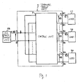
- Fig. 1 shows the structure of a terminal table unit 1 embodying this invention, provided with a control unit 2, input terminals I1 and I2 for connecting a DC power source unit PS and output terminals A1, B1-An, Bn for branching the DC voltage VD supplied from the DC power source unit PS to supply DC voltage VD and load currents IL1-ILn respectively to loads L1-Ln.
- the control unit 2 is for controlling not only the timing of connecting and disconnecting the DC power source (DC voltage VD) to be supplied to the loads L1-Ln through each of the output terminals (power supply terminals) A1, B1-An, Bn but also the display of the current and voltage values and the reporting on overcurrents.
- Fig. 2 is a block diagram of this control unit 2.
- the control unit 2 will be explained in terms of only one of its blocks (channel CH1) for supplying DC power source (DC voltage VD) from the output terminals A1, B1 to the load L1 but the other blocks (channel CH2 - channel CHn) for supplying the DC power (DC voltage VD) are of the same structure.
- control unit 2 is provided with a control means 3, a sequence means 4 included in the control means 3, a current detecting means 5, a voltage detecting means 6, a switching means 7, a display means 8, a reporting means 9, a setting means 10 and a memory means 11.
- the control means 3 is based on a microcomputer and, being provided with A/D conversion function, calculation functions of various kinds, comparison function, timer function and processing function, is adapted to supply switch data DS to the switching means 7 on the basis of data determined by the sequence means 4 to switch on and off the switch elements 7a and 7b and to connect and disconnect the DC voltage VD between output lines LP and LM to the output terminals A1 and B1 at the set timing.
- the control means 3 also serves to compare the converted voltage Vd (obtained by converting the load current IL1 from the current detecting means 5) with a voltage value stored in the memory means 11, to supply report data DT to the reporting means 9 to have an alarm sounded to make a report that an abnormal current is flowing through the load L1 if the converted voltage Vd is found to exceed a voltage value corresponding to an overcurrent IK.
- a transistor and a relay are also activated on the basis of the report data DT to output an electric signal so as to control external display and alarm devices to display and output a warning that there is an abnormal current.
- the control means 3 supplies the switch data DS to the switching means 7 to switch off the switch elements 7a and 7b and thereby disconnect the DC voltage VD between output lines LP and LM from the output terminals A1 and A2.
- the control means 3 compares the detected voltage VP provided from the voltage detecting means 6 with the voltage value stored in the memory means 11. If the detected voltage VP remains in excess of a voltage value (such as 22V) close to the constant value (such as 24V) of the DC voltage VD over a specified length of time, the control means 3 supplies the switch data DS to the switching means 7 to thereby switch on the switch elements 7a and 7b and drives the load L1 at a normal voltage from the initial supply time of the DC voltage.
- a voltage value such as 22V
- the constant value such as 24V
- the control means 3 supplies the switch data DS to the switching means 7 to thereby switch off the switch elements 7a and 7b and carries out a control such that the load L1 is not driven under the condition of abnormal DC voltage.
- Another control carried out by the control means 3 is to supply display data DG based on the converted voltage Vd provided from the current detecting means 5 and the detected voltage VP provided from the voltage detecting means 6 and to thereby cause the load current IL1 inclusive of the overcurrent IK and the DC voltage VD to be displayed on the display means 8 in terms respectively of a current value and a voltage value.
- the control means 3 further serves to carry out the control of having setting data JS supplied from the setting means 10 such as the timing data for connecting and disconnecting the supply of the DC voltage VD, overcurrent value data of the overcurrent IK on a plurality of levels, the lower limit data on the start of supplying the DC voltage VD, the upper limit data on the stopping the supply of the DC voltage VD, the overcurrent value data of the overcurrent IK against rush current IR and the timing data of the continuing time to be stored by the memory means 11 as memory data JM.
- setting data JS supplied from the setting means 10 such as the timing data for connecting and disconnecting the supply of the DC voltage VD, overcurrent value data of the overcurrent IK on a plurality of levels, the lower limit data on the start of supplying the DC voltage VD, the upper limit data on the stopping the supply of the DC voltage VD, the overcurrent value data of the overcurrent IK against rush current IR and the timing data of the continuing time to be stored by the memory means 11 as memory data JM.
- the control means 3 also serves to supply the set data JS from the setting means 10 or the memory data JM from the memory means 11 to the display means 8 as display data DG and to cause information and data of different kinds to be displayed on the display means 8.
- the control means 3 carries out the control of not making any report on the over current 1K or shutting off the power supply on the basis of the detected overcurrent IK and its transient time ⁇ although the current detecting means 6 may detect an overcurrent IK.
- the sequence means 4 is provided with an ordering function and a timer function and is adapted to generate switch data DS for switching on and off the switch elements 7a and 7b of the switching means 7 on the basis of the set data JS from the setting means 10.
- the sequence means 4 serves to monitor the value of the overcurrent IK supplied from the current detecting means 5 and the transient time ⁇ .
- the rush current IR may exceed the value of the overcurrent IK, if it is less than a specified transient time ⁇ , the generation of the switch data DS which would normally take place to switch off the switch elements 7a and 7b of the switching means 7 is inhibited and the DC voltage VD is continuously supplied to the load L1 such that the shutting off of the DC source caused by a rush current IR which would necessarily be generated in the initial condition as the DC source (DC voltage VD) is applied to a capacitive load is prevented from occurring.
- the current detecting means 5 comprises a resistor r inserted into the output line LM and a differential amplifier for amplifying the voltage drop due to the load current IL1 through the resistor r and is adapted to detect the load current IL1 as a corresponding converted voltage Vd and to output it to the control means 3.
- the voltage detecting means 6 serves to reduce the DC voltage VD between the output lines LP and LM by resistive voltage division or by means of a differential amplifier, to detect the reduced DC voltage as detection voltage VP and to output it to the control means 3.
- the switching means 7 is formed with semiconductor switches such as relays, MOSFETs and transistors and is inserted into the output lines LP and LM, serving to switch the switch elements 7a and 7b on (as shown by solid lines) or off (as shown by broken lines) so as to connect and to disconnect the DC source to and from the output terminals A1 and B1.
- the switch elements 7a and 7b correspond to relay contact points, the drain and the source of a MOSFET and the collector and the emitter of a transistor, and the relay and the semiconductor switch may be switched on and off by supplying switch data DS to the relay coil, the FET gate or the base of the transistor.
- the display means 8 may be formed with a display driver circuit and an LCD (liquid crystal display) and serves to generate a display driver signal in response to the display data DG supplied from the control means 3 and to display a current value or a voltage value on the LCD.
- the display means 8 may be provided with a plurality of light emitting diodes (LEDs) and adapted to activate a blue light emitting diode when the switching means 7 is in the switched-on condition and to activate a red light emitting diode when the switching means 7 is in the switched-off condition.
- LEDs light emitting diodes
- the reporting means 9 is comprised of an oscillator and a speaker and serves to generate an alarm signal in response to communication data DT supplied from the control means 3, causing an alarm sound to be emitted to report an abnormal condition in the DC voltage VD or the load current IL1.
- the setting means 10 is comprised of a key, a volume or a rotary switch and serves to supply set data JS for setting and changing the timing data for the connection and disconnection of the DC source, the overcurrent value data of the overcurrent IK on a plurality of levels, the lower limit voltage data for starting supply of DC voltage VD, the upper limit voltage data for stopping the supply, the overcurrent value data of the over current IK corresponding to the rush current IR and the timing data of the transient time ⁇ .
- the terminal table unit 2 is provided with such a setting means 10 for setting or changing the timing for connecting and disconnecting the source (DC voltage VD) and the overcurrent value IK, the timing for connecting and disconnecting the DC source (DC voltage VD) to be supplied to the load L1 as well as the overcurrent value IK for disconnecting the DC power source (DC voltage VD) can be freely changed according to the desires of the users and hence the degree of freedom of the unit can be expanded.
- the memory means 11 may comprise a fixed memory such as a ROM or a rewritable memory such as a flash memory and serves to store as the memory data JM the timing data on the connection and disconnection of the DC source, overcurrent value data on the plurality of levels of the overcurrent IK, the lower limit voltage data for the start of supply of the DC voltage VD, the upper limit voltage data for stopping the supply, the overcurrent value data of the overcurrent IK corresponding to the rush current IR and the timing data of continuing time, based on the set data JS from various control programs and the setting means 10.
- the memory means 11 also serves to provide the memory data JM to the control means 3.
- control unit 2 since the control unit 2 according to this invention is not only adapted to store the overcurrent IK value for beginning a report and the overcurrent data of the overcurrent IK value for switching off the switching means 7 but also provided with a memory means 11 for storing the sequence data on connecting and disconnecting the power source, reporting on the overcurrent, disconnection of the DC source corresponding to the overcurrent and the sequence of connection and disconnection can be freely set and acted upon.
- control means 3 the reporting means 9, the setting means and the memory means 11 belonged to one block (channel CH1)
- control unit 2 is further provided with a sequence means 4 for determining the timing for connecting and disconnecting the power source, a current detecting means 5 for detecting a current (the load current IL1 ), a voltage detecting means 6 for detecting a terminal voltage (DC voltage VD), switching means 7 for connecting and disconnecting the DC source (DC voltage VD), a display device 8 for displaying current and voltage values, a reporting means 9 for reporting on overcurrent IK and an abnormal voltage, and a control means 3 for controlling the overall operation of the unit, the timing for connecting and disconnecting the power source can be set according to the load L1 and the current and voltage values during the operation can be displayed as well as the occurrence of an overcurrent for an improved convenience to the user.
- a sequence means 4 for determining the timing for connecting and disconnecting the power source
- a current detecting means 5 for detecting a current (the load current IL1 )
- a voltage detecting means 6 for detecting a terminal voltage (DC voltage VD)
- switching means 7 for connecting and disconnect
- Figs. 3A, 3B, 3C and 3D together referred to as Fig. 3, show the function of preventing rush current as one of the embodiments of the control means according to this invention.
- Fig. 3A shows the load current characteristic when there is no function of preventing rush current
- Figs, 3B, 3C and 3D show the time-load current characteristics of channels CH1-CH3, respectively each having the function of preventing rush current. It will be explained below on the assumption that loads L1-L3 are operated and load currents IL1-IL3 flow in channels CH1-CH3.
- Fig. 3A shows a situation without the function of preventing rush current.
- the DC power source device PS is provided with the function of preventing rush current and if this function is assumed to operate even when there is a rush current exceeding the value of Ir shown in Fig. 3A and lasting for a time shorter than its transient (setting) time T ⁇ , this function comes into play before the elapse of this transient time T ⁇ after the DC voltage VD is applied to the load having the load current characteristic shown by Fig. 3A and the power supply to the terminal table unit 1 is stopped.
- the times at which the application of DC power source (DC voltage VD) is started to the loads L1-L3 are indicated as t1, t2 and t3 and the final constant current values are indicated respectively by IM1, IM2 and IM3.
- the control means 3 including the sequence means 4 controls the switch elements 7a and 7b of the switching means 7 to be switched off and the supply of the DC voltage VD to the loads L1-L3 is stopped.
- the DC voltage VD can be supplied continuously to the loads L1-L3 without stopping the load currents IL1-IL3 because none of the rush current limiting values IR1-IR3 exceeds the transient time ⁇ .
- the wave height of the rush current of the load currents IL1-IL3 can be kept low and the transient time of the wave height can be reduced such that it can be treated like a load with a normal current passing through without activating the overcurrent preventing function of the DC power source device PS.
- the control means 3 of this invention can carry out a control based on the detected overcurrent IK and the transient time ⁇ such that no reporting on the overcurrent is made and the power source is not disconnected.
- the supply of power can be continued to the load although the rush current IR flows into the capacitive load and a stable power supply can be maintained without adversely affecting reliability.
- the terminal table unit 1 serves to receive DC power supplied from a power source device PS and to distribute it among a plurality of loads L1-Ln and is adapted to control the timing for connecting and disconnecting the DC power source and the threshold current value for disconnection, and since a control unit 2 is provided for controlling the display of current and voltage values and the reporting on an overcurrent and an abnormal voltage, the user can freely set the condition of the DC source power supplied to the loads and easily observe the condition of operation of the DC power source.
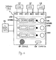
- Fig. 4 shows an external image of an example of terminal table unit embodying this invention with the unit 1 structured as having three channels CH1-CH3 for supplying DC power to loads L1-L3.
- the channels CH1-CH3 are each provided with a liquid crystal display LCD for displaying current and voltage values, a blue light emitting diode LED(B) for indicating that the load current is normal, a red light emitting diode LED(R) for indicating that the load current is abnormal and a knob VR for setting and selecting various data.
- a speaker SP is provided for generating a sound in common for all three channels CH1-CH3.
- a connector CN to a personal computer is provided such that various data may be set through a personal computer connected through the connector CN.
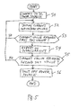
- Step S1 After a DC power source is connected at a specified timing by means of the sequence means 4, the control means 3 and the switching means 7 (Step S1), current and voltage values are displayed by the current detecting means 5, the voltage detecting means 6, the control means 3 and the display means 8 (Step S2). If it is determined by the control means 3 that the current value exceeds a first set (threshold) value (YES in Step S3) which is an overcurrent value preliminarily set by the user, a report is made to the effect of an overcurrent (Step S4) by the control means 3 and the reporting means 9.
- Step S5 a second set (threshold) value
- the power source is shut off (Step S6) by the control means 3 and the switching means 7.
- the aforementioned first set value is not as high as being dangerous such that it is sufficient to merely make a report on it but the second value is sufficiently high to be dangerous enough such that the supply of power should be stopped. If the current value does not exceed the second set value (NO in Step S5), the routine goes back to Step S2.
- the unit is provided with an improved reliability. It now goes without saying that the present invention is applicable to terminal table units of all kinds adapted to receive DC power from a power source unit and distribute it to a plurality of loads.
Landscapes
- Engineering & Computer Science (AREA)
- Power Engineering (AREA)
- Business, Economics & Management (AREA)
- Emergency Management (AREA)
- Physics & Mathematics (AREA)
- General Physics & Mathematics (AREA)
- Direct Current Feeding And Distribution (AREA)
- Emergency Protection Circuit Devices (AREA)
- Devices For Supply Of Signal Current (AREA)
- Power Sources (AREA)
Applications Claiming Priority (2)
| Application Number | Priority Date | Filing Date | Title |
|---|---|---|---|
| JP2004064600 | 2004-03-08 | ||
| JP2004064600 | 2004-03-08 |
Publications (1)
| Publication Number | Publication Date |
|---|---|
| EP1575145A1 true EP1575145A1 (fr) | 2005-09-14 |
Family
ID=34824538
Family Applications (1)
| Application Number | Title | Priority Date | Filing Date |
|---|---|---|---|
| EP05003911A Withdrawn EP1575145A1 (fr) | 2004-03-08 | 2005-02-23 | Dispositif et methode de contrôle de charge à multiples canaux |
Country Status (5)
| Country | Link |
|---|---|
| US (2) | US20050195546A1 (fr) |
| EP (1) | EP1575145A1 (fr) |
| KR (1) | KR100676605B1 (fr) |
| CN (1) | CN1667908A (fr) |
| TW (1) | TWI305695B (fr) |
Families Citing this family (15)
| Publication number | Priority date | Publication date | Assignee | Title |
|---|---|---|---|---|
| JP2005197177A (ja) * | 2004-01-09 | 2005-07-21 | Fujitsu Ltd | 駆動装置及び方法 |
| US8231056B2 (en) * | 2005-04-08 | 2012-07-31 | Authentec, Inc. | System for and method of protecting an integrated circuit from over currents |
| CN101228396B (zh) * | 2005-07-26 | 2010-06-23 | 京瓷株式会社 | 钎焊构造体、陶瓷加热器以及热线点火塞 |
| JP4201050B2 (ja) | 2006-10-11 | 2008-12-24 | トヨタ自動車株式会社 | 電気負荷制御装置及び電気負荷制御方法、並びに電動負荷制御装置及び電動負荷制御方法 |
| CN101373395B (zh) * | 2007-08-24 | 2013-01-09 | 鸿富锦精密工业(深圳)有限公司 | 电源报警电路 |
| JP2010263730A (ja) * | 2009-05-11 | 2010-11-18 | Funai Electric Co Ltd | Usb電源回路 |
| KR101023336B1 (ko) * | 2009-07-03 | 2011-03-18 | 삼성전기주식회사 | 로드 쉐어링 장치 및 이를 구비한 병렬 전원 공급 장치 |
| KR101040472B1 (ko) * | 2009-12-10 | 2011-06-09 | 한전케이피에스 주식회사 | 다중전원공급장치의 시험을 위한 단자박스 |
| TWI410029B (zh) * | 2009-12-31 | 2013-09-21 | Delta Electronics Inc | 具可控制能量釋放功能之多組輸出降壓型轉換裝置 |
| JP5506937B2 (ja) * | 2010-08-24 | 2014-05-28 | 三菱電機株式会社 | 電力変換装置 |
| US20140175877A1 (en) * | 2012-08-13 | 2014-06-26 | William Baker | Building Power Management System |
| EP3030941B1 (fr) * | 2013-08-06 | 2018-10-31 | Bedrock Automation Platforms Inc. | Module programmable pour des systèmes de commande industriels |
| TWI540419B (zh) * | 2013-11-20 | 2016-07-01 | 鴻海精密工業股份有限公司 | 電子裝置 |
| JP6839777B2 (ja) * | 2018-01-19 | 2021-03-10 | シャープNecディスプレイソリューションズ株式会社 | 電子機器及び電子機器の電源管理方法 |
| US11201466B2 (en) * | 2018-07-12 | 2021-12-14 | Globalfoundries U.S. Inc. | Electrostatic discharge clamp structures |
Citations (5)
| Publication number | Priority date | Publication date | Assignee | Title |
|---|---|---|---|---|
| US4890212A (en) * | 1986-10-23 | 1989-12-26 | Minolta Camera Kabushiki Kaisha | Electric apparatus having a start-up control function |
| EP0415441A2 (fr) * | 1989-08-31 | 1991-03-06 | Mita Industrial Co. Ltd. | Sous-système de réglage pour l'alimentation en courant électrique d'un appareil de formation d'images |
| EP1046545A2 (fr) * | 1999-04-22 | 2000-10-25 | Harness System Technologies Research, Ltd. | Dispositif pour contrôler le système d'alimentation électrique d'un véhicule |
| US20030086228A1 (en) * | 2001-11-06 | 2003-05-08 | Papallo Thomas F | Compact low AMP electronic circuit breaker or residential load center |
| WO2003098403A2 (fr) * | 2002-05-16 | 2003-11-27 | Honeywell International Inc. | Centre de gestion des charges électriques |
Family Cites Families (8)
| Publication number | Priority date | Publication date | Assignee | Title |
|---|---|---|---|---|
| EP0046545A1 (fr) * | 1980-08-21 | 1982-03-03 | BROWN, BOVERI & CIE Aktiengesellschaft | Equipement d'installation électrique |
| US5327016A (en) * | 1992-04-06 | 1994-07-05 | Motorola, Inc. | Load control circuit including automatic AC/DC discernment |
| JPH0630145A (ja) * | 1992-07-13 | 1994-02-04 | Hitachi Ltd | ホームバスシステム |
| US5502374A (en) * | 1994-09-02 | 1996-03-26 | Veris Industries, Inc. | Current sensors |
| KR960043444A (ko) * | 1995-05-04 | 1996-12-23 | 박광선 | 복수의 부하를 선택적으로 지연 오프 시킬 수 있는 전원 제어 스위치 장치 |
| KR200147001Y1 (ko) * | 1996-12-27 | 1999-06-15 | 배섭 | 전동드라이버 제어기 |
| US6289267B1 (en) * | 1998-03-19 | 2001-09-11 | Siemens Energy & Automation, Inc. | Graphical energy information display system having a menu for user selection of energy related information for an AC load control device |
| US6469882B1 (en) * | 2001-10-31 | 2002-10-22 | General Electric Company | Current transformer initial condition correction |
-
2005
- 2005-02-16 US US11/060,468 patent/US20050195546A1/en not_active Abandoned
- 2005-02-23 EP EP05003911A patent/EP1575145A1/fr not_active Withdrawn
- 2005-03-03 KR KR1020050017629A patent/KR100676605B1/ko not_active Expired - Fee Related
- 2005-03-04 TW TW094106529A patent/TWI305695B/zh not_active IP Right Cessation
- 2005-03-07 CN CNA2005100526342A patent/CN1667908A/zh active Pending
-
2006
- 2006-09-19 US US11/524,062 patent/US20070064361A1/en not_active Abandoned
Patent Citations (5)
| Publication number | Priority date | Publication date | Assignee | Title |
|---|---|---|---|---|
| US4890212A (en) * | 1986-10-23 | 1989-12-26 | Minolta Camera Kabushiki Kaisha | Electric apparatus having a start-up control function |
| EP0415441A2 (fr) * | 1989-08-31 | 1991-03-06 | Mita Industrial Co. Ltd. | Sous-système de réglage pour l'alimentation en courant électrique d'un appareil de formation d'images |
| EP1046545A2 (fr) * | 1999-04-22 | 2000-10-25 | Harness System Technologies Research, Ltd. | Dispositif pour contrôler le système d'alimentation électrique d'un véhicule |
| US20030086228A1 (en) * | 2001-11-06 | 2003-05-08 | Papallo Thomas F | Compact low AMP electronic circuit breaker or residential load center |
| WO2003098403A2 (fr) * | 2002-05-16 | 2003-11-27 | Honeywell International Inc. | Centre de gestion des charges électriques |
Also Published As
| Publication number | Publication date |
|---|---|
| CN1667908A (zh) | 2005-09-14 |
| TW200614621A (en) | 2006-05-01 |
| TWI305695B (en) | 2009-01-21 |
| US20070064361A1 (en) | 2007-03-22 |
| US20050195546A1 (en) | 2005-09-08 |
| KR20060043367A (ko) | 2006-05-15 |
| KR100676605B1 (ko) | 2007-01-30 |
Similar Documents
| Publication | Publication Date | Title |
|---|---|---|
| EP1575145A1 (fr) | Dispositif et methode de contrôle de charge à multiples canaux | |
| US7800870B2 (en) | Power protection apparatus and electronic control unit | |
| US20110085044A1 (en) | Image display apparatus with external-equipment-link unit | |
| US8772963B2 (en) | Device for supplying uninterruptible power | |
| US20100013442A1 (en) | Charging system, electronic circuit device including secondary cell, and power supply device for charging | |
| KR20120020481A (ko) | 발광 구동 장치, 디스플레이 장치 및 그 구동 방법 | |
| US8054601B2 (en) | Power supply control apparatus having a function supplying power supply voltage | |
| US20090033268A1 (en) | Power supply system with function of short circuit detection | |
| US7764480B2 (en) | Electronic device, and circuit and method for protecting the same | |
| KR20100024284A (ko) | 리셋 기능을 갖는 백라이트 유닛용 구동회로 | |
| US6972940B2 (en) | Power supply protection circuit | |
| US20090297362A1 (en) | Electrical system for a pump | |
| KR100482611B1 (ko) | 차량의 회로 이상 검출 시스템 및 방법 | |
| JP2005295791A (ja) | 端子台ユニット及びその制御方法 | |
| US11370320B2 (en) | Electronic control device for in-vehicle use | |
| JP2007013141A (ja) | ディスプレイ装置 | |
| JP4082547B2 (ja) | 発光素子の電源供給制御装置 | |
| US10338649B2 (en) | Fan control apparatus and method of operating the same | |
| JPH0759265A (ja) | 電池回路 | |
| US7474281B2 (en) | Multi-mode switch for plasma display panel | |
| KR101533463B1 (ko) | 전원공급회로 | |
| KR20060002289A (ko) | 이동통신 단말기의 전원 관리 장치 및 방법 | |
| JP3599084B2 (ja) | 電源装置 | |
| KR0121487Y1 (ko) | 밧데리상태 디스플레이장치 | |
| KR20070037072A (ko) | 이동통신단말기의 led 밝기 레벨 제어 방법 및 이를위한 이동통신단말기 |
Legal Events
| Date | Code | Title | Description |
|---|---|---|---|
| PUAI | Public reference made under article 153(3) epc to a published international application that has entered the european phase |
Free format text: ORIGINAL CODE: 0009012 |
|
| AK | Designated contracting states |
Kind code of ref document: A1 Designated state(s): AT BE BG CH CY CZ DE DK EE ES FI FR GB GR HU IE IS IT LI LT LU MC NL PL PT RO SE SI SK TR |
|
| AX | Request for extension of the european patent |
Extension state: AL BA HR LV MK YU |
|
| 17P | Request for examination filed |
Effective date: 20060310 |
|
| AKX | Designation fees paid |
Designated state(s): DE FR GB IT |
|
| 17Q | First examination report despatched |
Effective date: 20060629 |
|
| STAA | Information on the status of an ep patent application or granted ep patent |
Free format text: STATUS: THE APPLICATION IS DEEMED TO BE WITHDRAWN |
|
| 18D | Application deemed to be withdrawn |
Effective date: 20080216 |